EP0656654A2 - Procédés de fabrication de cellules DRAM à sillon comportant une plaque de substrat à faible courant de fuite et dispositifs obtenus par ce procédé - Google Patents
Procédés de fabrication de cellules DRAM à sillon comportant une plaque de substrat à faible courant de fuite et dispositifs obtenus par ce procédé Download PDFInfo
- Publication number
- EP0656654A2 EP0656654A2 EP94117743A EP94117743A EP0656654A2 EP 0656654 A2 EP0656654 A2 EP 0656654A2 EP 94117743 A EP94117743 A EP 94117743A EP 94117743 A EP94117743 A EP 94117743A EP 0656654 A2 EP0656654 A2 EP 0656654A2
- Authority
- EP
- European Patent Office
- Prior art keywords
- trench
- substrate
- region
- forming
- nitride
- Prior art date
- Legal status (The legal status is an assumption and is not a legal conclusion. Google has not performed a legal analysis and makes no representation as to the accuracy of the status listed.)
- Withdrawn
Links
- 239000000758 substrate Substances 0.000 title claims abstract description 94
- 238000000034 method Methods 0.000 title claims abstract description 64
- 238000009792 diffusion process Methods 0.000 claims abstract description 39
- 239000000463 material Substances 0.000 claims abstract description 27
- 238000005530 etching Methods 0.000 claims abstract description 17
- 239000002019 doping agent Substances 0.000 claims abstract description 15
- 238000000151 deposition Methods 0.000 claims abstract description 14
- 239000011810 insulating material Substances 0.000 claims abstract description 8
- 239000010410 layer Substances 0.000 claims description 109
- 150000004767 nitrides Chemical class 0.000 claims description 76
- 238000003860 storage Methods 0.000 claims description 39
- VYPSYNLAJGMNEJ-UHFFFAOYSA-N Silicium dioxide Chemical compound O=[Si]=O VYPSYNLAJGMNEJ-UHFFFAOYSA-N 0.000 claims description 15
- 229910021420 polycrystalline silicon Inorganic materials 0.000 claims description 14
- 229920005591 polysilicon Polymers 0.000 claims description 12
- 239000011521 glass Substances 0.000 claims description 10
- 239000004065 semiconductor Substances 0.000 claims description 9
- 229910052710 silicon Inorganic materials 0.000 claims description 9
- 239000010703 silicon Substances 0.000 claims description 9
- 239000011241 protective layer Substances 0.000 claims description 6
- 235000012239 silicon dioxide Nutrition 0.000 claims description 6
- 239000000377 silicon dioxide Substances 0.000 claims description 6
- QGZKDVFQNNGYKY-UHFFFAOYSA-N Ammonia Chemical compound N QGZKDVFQNNGYKY-UHFFFAOYSA-N 0.000 claims description 4
- 229910052581 Si3N4 Inorganic materials 0.000 claims description 4
- 229910052785 arsenic Inorganic materials 0.000 claims description 4
- RQNWIZPPADIBDY-UHFFFAOYSA-N arsenic atom Chemical compound [As] RQNWIZPPADIBDY-UHFFFAOYSA-N 0.000 claims description 4
- 230000000873 masking effect Effects 0.000 claims description 4
- HQVNEWCFYHHQES-UHFFFAOYSA-N silicon nitride Chemical compound N12[Si]34N5[Si]62N3[Si]51N64 HQVNEWCFYHHQES-UHFFFAOYSA-N 0.000 claims description 4
- ZOXJGFHDIHLPTG-UHFFFAOYSA-N Boron Chemical compound [B] ZOXJGFHDIHLPTG-UHFFFAOYSA-N 0.000 claims description 3
- 229910052796 boron Inorganic materials 0.000 claims description 3
- 230000005669 field effect Effects 0.000 claims description 3
- 229910052814 silicon oxide Inorganic materials 0.000 claims description 3
- 229910021529 ammonia Inorganic materials 0.000 claims description 2
- 229910052787 antimony Inorganic materials 0.000 claims description 2
- WATWJIUSRGPENY-UHFFFAOYSA-N antimony atom Chemical compound [Sb] WATWJIUSRGPENY-UHFFFAOYSA-N 0.000 claims description 2
- 229910052738 indium Inorganic materials 0.000 claims description 2
- APFVFJFRJDLVQX-UHFFFAOYSA-N indium atom Chemical compound [In] APFVFJFRJDLVQX-UHFFFAOYSA-N 0.000 claims description 2
- 238000010438 heat treatment Methods 0.000 claims 2
- 230000001590 oxidative effect Effects 0.000 claims 2
- BHEPBYXIRTUNPN-UHFFFAOYSA-N hydridophosphorus(.) (triplet) Chemical compound [PH] BHEPBYXIRTUNPN-UHFFFAOYSA-N 0.000 claims 1
- 230000003647 oxidation Effects 0.000 abstract description 9
- 238000007254 oxidation reaction Methods 0.000 abstract description 9
- 230000003071 parasitic effect Effects 0.000 description 15
- 239000003990 capacitor Substances 0.000 description 11
- 238000004519 manufacturing process Methods 0.000 description 8
- XUIMIQQOPSSXEZ-UHFFFAOYSA-N Silicon Chemical compound [Si] XUIMIQQOPSSXEZ-UHFFFAOYSA-N 0.000 description 6
- 238000001020 plasma etching Methods 0.000 description 6
- NBIIXXVUZAFLBC-UHFFFAOYSA-N Phosphoric acid Chemical compound OP(O)(O)=O NBIIXXVUZAFLBC-UHFFFAOYSA-N 0.000 description 4
- 238000005229 chemical vapour deposition Methods 0.000 description 3
- 229920002120 photoresistant polymer Polymers 0.000 description 3
- 229910000147 aluminium phosphate Inorganic materials 0.000 description 2
- QVGXLLKOCUKJST-UHFFFAOYSA-N atomic oxygen Chemical compound [O] QVGXLLKOCUKJST-UHFFFAOYSA-N 0.000 description 2
- 239000005380 borophosphosilicate glass Substances 0.000 description 2
- 238000004140 cleaning Methods 0.000 description 2
- 229910052760 oxygen Inorganic materials 0.000 description 2
- 239000001301 oxygen Substances 0.000 description 2
- 230000001681 protective effect Effects 0.000 description 2
- 239000007787 solid Substances 0.000 description 2
- 208000012868 Overgrowth Diseases 0.000 description 1
- OAICVXFJPJFONN-UHFFFAOYSA-N Phosphorus Chemical compound [P] OAICVXFJPJFONN-UHFFFAOYSA-N 0.000 description 1
- 229910052782 aluminium Inorganic materials 0.000 description 1
- XAGFODPZIPBFFR-UHFFFAOYSA-N aluminium Chemical compound [Al] XAGFODPZIPBFFR-UHFFFAOYSA-N 0.000 description 1
- 238000000137 annealing Methods 0.000 description 1
- 238000003491 array Methods 0.000 description 1
- 230000015572 biosynthetic process Effects 0.000 description 1
- 239000002131 composite material Substances 0.000 description 1
- 230000007423 decrease Effects 0.000 description 1
- 230000008021 deposition Effects 0.000 description 1
- 238000000469 dry deposition Methods 0.000 description 1
- 238000005516 engineering process Methods 0.000 description 1
- 230000036039 immunity Effects 0.000 description 1
- 238000009413 insulation Methods 0.000 description 1
- 150000002500 ions Chemical class 0.000 description 1
- 230000014759 maintenance of location Effects 0.000 description 1
- 229910052751 metal Inorganic materials 0.000 description 1
- 239000002184 metal Substances 0.000 description 1
- 238000001465 metallisation Methods 0.000 description 1
- 239000011574 phosphorus Substances 0.000 description 1
- 229910052698 phosphorus Inorganic materials 0.000 description 1
- 238000004151 rapid thermal annealing Methods 0.000 description 1
- 239000002356 single layer Substances 0.000 description 1
- 238000009987 spinning Methods 0.000 description 1
- WFKWXMTUELFFGS-UHFFFAOYSA-N tungsten Chemical compound [W] WFKWXMTUELFFGS-UHFFFAOYSA-N 0.000 description 1
- 229910052721 tungsten Inorganic materials 0.000 description 1
- 239000010937 tungsten Substances 0.000 description 1
Images



Classifications
-
- H—ELECTRICITY
- H10—SEMICONDUCTOR DEVICES; ELECTRIC SOLID-STATE DEVICES NOT OTHERWISE PROVIDED FOR
- H10B—ELECTRONIC MEMORY DEVICES
- H10B12/00—Dynamic random access memory [DRAM] devices
- H10B12/30—DRAM devices comprising one-transistor - one-capacitor [1T-1C] memory cells
- H10B12/37—DRAM devices comprising one-transistor - one-capacitor [1T-1C] memory cells the capacitor being at least partially in a trench in the substrate
Definitions
- the present invention relates generally to a method for making an improved trench for a semiconductor memory device and the device formed thereby and, more particularly, to a method for fabricating a low leakage trench for a Dynamic Random Access Memory (DRAM) cell wherein trench parasitic sidewall leakage currents from a bitline contact to the storage node and from the storage node to the substrate are eliminated by an insulating or diffusion ring surrounding an upper portion of the trench.
- DRAM Dynamic Random Access Memory
- VLSI Very Large Scale Integrated
- DRAM cells in the time frame of 4Mbit and beyond require trench storage capacitors in order to meet high density requirements.
- DRAM cells having a storage capacitor disposed in a trench formed in a semiconductor substrate are known in the art.
- U.S. Patent No. 4,688,063 assigned to the same assignee as the present invention which patent is hereby incorporated by reference, discloses a substrate plate trench (SPT) DRAM cell which utilizes a trench storage capacitor formed in a semiconductor substrate.
- the SPT DRAM cell includes a field effect access transistor disposed in a well which is opposite in conductivity type to that of the substrate.
- the trench capacitor extends from the surface of the well, through the well and lightly doped substrate portion, into the heavily doped portion of the substrate.
- the capacitor electrode disposed in the trench is directly connected to the source/drain of the access transistor.
- Trench DRAM cells suffer from two main disadvantages resulting from a parasitic sidewall leakage current.
- the two disadvantages are the trench parasitic sidewall leakage through the trench sidewalls (1) from the bitline contact to the storage node and (2) from the storage node to the substrate.
- SPT Substrate Plate Trench Capacitor
- the DRAM cell of U.S. Patent 4,688,063 includes an n-well interposed between the substrate plate and the access transistor electrodes.
- an n-well with a doping profile that monotonically decreases with depth can be utilized.
- these improvements do not significantly reduce the trench parasitic sidewall leakage currents.
- Another way to reduce the parasitic sidewall leakage currents is by increasing the thickness of an oxide collar formed within an upper portion of the trench.
- increasing the collar thickness reduces the contact area available for contact, increases the RC time constant of the storage node polysilicon and introduces process constraints.
- a further way to reduce the sidewall leakage currents is disclosed in a co-pending application, assigned to the same assignee as the present application, Serial No. 696,691, filed May 7, 1991.
- the application discloses an SPT DRAM cell which includes a buried oxide collar surrounding an upper portion of the trench of the storage capacitor and extends from the n-well through the n-well and into a lightly doped portion of the substrate.
- the oxide collar is contiguous with an insulating layer formed within the trench on all sides.
- this DRAM cell does not reduce the leakage current from the storage node to the bitline contact.
- this DRAM cell results in additional leakage problems.
- the method for fabricating this DRAM cell includes forming a thick oxide layer on an upper portion of the substrate.
- the oxide layer is then buried within an upper portion of the substrate by conventional epitaxial overgrowth technology.
- a trench is then dug down to and through the buried oxide layer and the substrate such that the oxide layer completely surrounds an upper portion of the trench.
- U.S. Patent 4,987,470 discloses a DRAM device which includes a field shield conducting layer placed inside a trench to prevent parasitic sidewall leakage through the trench sidewalls.
- the conductive shield layer is disposed between the trench sidewall and the storage node with insulating material between them.
- the conductive layer shields the field from the storage polysilicon.
- the use of the shield layer within the trench does not substantially prevent parasitic leakage currents.
- the present invention is directed to methods for fabricating a low leakage trench for a DRAM cell and the devices formed thereby wherein trench parasitic sidewall leakage currents from a bitline contact to the storage node and from the storage node to the substrate are substantially reduced by an insulating or diffusion ring surrounding an upper portion of the trench.
- the starting structure for all the methods of the present invention is a substrate of a first conductivity type having a lightly doped upper portion and a heavily doped lower portion.
- a nitride/oxide protective layer is deposited on the substrate.
- a trench is etched at a first region to a first depth which is more than the expected source/drain depth but less than the expected n-well depth.
- a nitride collar is then formed on the vertical surfaces of the trench.
- the trench is then etched to a second depth which is still less than the expected n-well depth.
- a layer of doped material having a dopant of the second conductivity type is deposited within the trench. The dopant is then outdiffused into the trench sidewalls to form a diffusion ring of the second conductivity type extending from the nitride collar and within the upper portion of the substrate.
- the doped material remaining in the trench is removed.
- the trench is then etched to a third and final depth into the lower portion of the substrate such that said diffusion ring surrounds an upper portion of the trench.
- the diffusion ring is contiguous with the trench on all sides and not within the trench. Thereafter, conventional DRAM processing techniques are utilized to complete the DRAM cell of the present invention.
- one of the sides of the trench is selectively doped all the way to the surface of the substrate to further reduce the leakage from the storage node to the bitline contact.
- a planarization resist is formed within the trench.
- a photoresist and masking step is then used to expose one side of the nitride layer.
- the exposed portion of the nitride layer is then removed.
- the trench is then etched to the second depth and a layer of doped material with the second conductivity dopant is deposited in the trench.
- the dopant is outdiffused to form a second conductivity type diffusion ring surrounding a portion of the trench, contiguous with the trench on all sides and extending to the surface of the substrate on the side of the trench where the nitride layer was removed.
- the remaining doped material is removed and the trench etched to its final depth. From this point, the conventional DRAM process is carried out to complete the DRAM cell of the present invention.
- Another embodiment of the present invention is directed to a method for fabricating a DRAM cell wherein an insulating ring surrounding an upper portion of the trench is utilized to reduce trench parasitic sidewall leakage currents.
- a layer of oxide is thermally grown on all vertical and horizontal surfaces of the trench.
- a nitride layer is then formed on the lower vertical and horizontal surfaces of the trench.
- a further nitride layer is then formed on the uppermost vertical surfaces of the trench thereby leaving an upper portion of the trench sidewalls between the two nitride layers exposed.
- the silicon not protected by the two nitride layers i.e., in the upper portion of the trench
- the insulating ring can be comprised of a material such as an oxide or oxynitride.
- the nitride layers are removed and another nitride layer is formed on all surfaces of the trench.
- the trench is then etched to a second and final depth to extend within the lower portion of the substrate such that the insulating ring surrounds an upper portion of the trench.
- the insulating ring is contiguous with the trench on all sides and not within the trench.
- the exposed silicon sidewalls of the trench between the two nitride layers is isotropically etched to form a sidewall shallow trench.
- the sidewall shallow trench is then filled with an insulating material to form the insulating ring of the present invention.
- Suitable materials for this insulating ring include an oxide, oxynitride or silicon nitride.
- one of the sides of the trench is selectively oxidized all the way to the surface of the substrate.
- one side of the nitride layer on the uppermost vertical surface of the trench is removed prior to oxidation.
- the resulting insulating ring includes one side which extends to the surface of the substrate.
- a protective nitride collar is then formed around the trench to protect the insulating ring and the trench is etched to its final depth. Subsequently, the conventional DRAM process is carried out to complete the DRAM cell of the present invention.
- FIGS. 1-5 are cross-sectional views showing the fabrication of one embodiment of a DRAM cell of the present invention at successive stages in accordance with one embodiment of the method of the present invention.
- FIGS. 6-9 are cross-sectional views showing the fabrication of another embodiment of a DRAM cell of the present invention at successive stages in accordance with another embodiment of the method of the present invention.
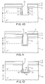
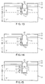
- FIGS. 10-17 are cross-sectional views showing the fabrication of a further embodiment of a DRAM cell of the present invention at successive stages in accordance with a further embodiment of the method of the present invention.
- FIG. 18 is a cross-sectional view of an alternative embodiment of the method of the present invention for fabricating the DRAM cell of FIG. 17.
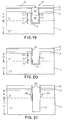
- FIGS. 19-21 are cross-sectional views showing the fabrication of another embodiment of a DRAM of the present invention at successive stages in accordance with another embodiment of the method of the present invention.
- the present invention is directed to methods for fabricating trench DRAM cells and the devices formed thereby wherein a trench parasitic sidewall leakage current through the trench sidewall from a bitline contact to the storage node and from the storage node to the substrate is substantially reduced. While the methods of the present invention will be described in connection with forming a single substrate plate trench (SPT) DRAM cell, it should be understood that a plurality of SPT DRAM cells can be formed in the well and fabricated simultaneously therein in the same manner as described hereinbelow. It should also be understood that while the process will be described in connection with forming the DRAM cell in a p-type substrate (n-well) the features of the present invention may easily be adapted for forming the DRAM cell in an n-type substrate (p-well).
- SPT substrate plate trench
- FIGS. 1-5 there is shown cross-sectional views disclosing the fabrication of a DRAM cell of the present invention at successive stages in accordance with one embodiment of the method of the present invention.
- the fabrication of the DRAM cell of the present invention is begun by starting with a substrate 10 having a lightly doped upper portion 12 of a p- conductivity type and a heavily doped lower portion 14 of a p+ conductivity type.
- the substrate 10 can be a semiconductor material such as silicon.
- the substrate 10 shown in FIG. 1, having a substantially planar surface 16 is the starting point for the methods of the present invention.
- a layer of nitride 18 and a layer of oxide 20 is deposited on substrate 10 by any well known wet or dry deposition process.
- the structure 21 is patterned using a trench mask by well known techniques. As shown in FIG. 2, a trench 22 is etched into the upper portion 12 of substrate 10 in the unmasked portion. The trench is etched to a depth (typically 0.5 - 0.6 ⁇ m) more than the expected source/drain junction depth but less than the expected n-well depth.
- the trench can be etched by an anisotropic etching process such as plasma etching or reactive ion etching (RIE).
- RIE reactive ion etching
- the nitride layer 24 is anisotropically etched to remove portions of the nitride layer 24 formed in the horizontal surface 26 while retaining the vertical sections on the sidewalls of the trench 22 to create the nitride collar 24 shown in FIG. 2.
- the trench 22 is further etched to a second depth which is still less than the expected n-well depth.
- the second depth is preferably less than the expected n-well depth to avoid leakage problems which can arise due to the diffusion ring (described below) of the present invention extending through the n-well and into the lightly doped portion 12 of substrate 10.
- a layer 28 of a doped material having an n-type dopant 29 is deposited within trench 22 and the surface of the oxide layer 20.
- the layer 28 of doped material can be deposited by well known chemical vapor deposition (CVD) methods. Suitable materials for doped layer 28 include arsenic doped glass, phosphorus doped (phosphosilicate) glass and antimony doped glass.
- the next step is to out diffuse the dopant 29 (e.g., arsenic) into the trench sidewalls to form an n+ diffusion ring 30 surrounding a portion of the trench 22 and being contiguous with the trench 22 on all sides.
- Rapid thermal annealing or furnace diffusion can be used to out diffuse the dopant 29 and form the n+ diffusion ring 30.
- an annealing temperature between about 900 to 1200°C for about one to six hours can be used to form diffusion ring 30.
- the layer of doped material within trench 22 is isotropically etched and removed.
- the trench 22 is etched to a third and final depth through the upper portion 12 and into the lower portion 14 of substrate 10 to produce the trench 23 shown in FIG. 4.
- the method of the present invention fabricates a diffusion ring 30 surrounding an upper portion of trench 23, is contiguous with trench 23 on all sides and not within trench 23.
- the diffusion ring 30 reduces a horizontal trench parasitic sidewall leakage current from a bitline contact to the storage node and the leakage current from the storage node to the substrate by several orders of magnitude.
- FIG. 5 there is shown a cross-sectional view of a DRAM cell 32 of the present invention which includes diffusion ring 30.
- an insulation layer 34 is formed on the surface of trench 23.
- Layer 34 may be a single layer of silicon dioxide or preferably may be a composite triple layer made up of alternating layers of silicon dioxide, silicon nitride and silicon dioxide.
- An optional internal oxide collar 35 can be formed within an upper portion of trench 23. It should be noted that the collar 35 must not be fabricated too thick to avoid reducing the contact area and increasing the RC time constant of the storage node polysilicon.
- a layer of heavily doped polycrystalline silicon is then deposited in trench 23 using CVD with boron doping to produce a p+ storage node 36.
- the layer 36 is deposited in a thickness sufficient to fill trench 23.
- Substrate 10 is then subjected to an RIE planarization step to remove the polycrystalline layer everywhere down to the top of trench 23.
- the nitride layer 18 deposited during the formation of the trench 23 acts as an etch stop during the RIE planarization step.
- ions are implanted to form n-well 38 which extends beyond diffusion ring 30 within the upper portion 12 of substrate 10. As stated above, this avoids additional leakage problems which can be caused by allowing the diffusion ring 30 to extend through n-well 38 and into upper portion 12.
- recessed oxide (ROX) regions 40 are formed by thermal oxidation and isolates DRAM cell 32 electrically from other similar cells formed on substrate 10.
- bridge region or strap 42 and access transistor (e.g., a field effect transistor) 44 is formed having a source region 46, drain region 48 and gate 50.
- the gate 50 corresponds to a wordline of the cell 32 while a gate 51 corresponds to a passing wordline of another cell formed in substrate 10.
- the source 46 and storage node 36 are electrically and physically interconnected by the bridge region 42 which can be of heavily doped p+ polycrystalline silicon.
- boro-phospho silicate glass (BPSG) is deposited and reflowed to form layer 52.
- contacts are open, and M1 metallization is deposited and patterned to form bitline metal interconnection layer 54.
- Layer 54 may be aluminum or tungsten.
- n-well 38 a plurality of SPT DRAM cells 32 are normally formed in n-well 38 and fabricated simultaneously therein in the same manner as described hereinabove. It will also be understood that, while an n-well 38 has been shown in FIG. 5, a p-well may just as easily be used. Then, of course, the conductivity types of source 46 and drains 48 and substrate portions 12 and 14 should be changed to n-conductivity type. In addition, the diffusion ring 30 would be of p+ conductivity and the layer 28 of doped material would include a p-type dopant. Suitable materials for a p-type doped layer 28 include boron doped glass and indium doped glass.
- FIGS. 6-9 there is shown cross-sectional views of another embodiment of a DRAM cell of the present invention at successive stages in accordance with another embodiment of the method of the present invention.
- one of the sides of the trench away from the source/drain diffusion is selectively doped all the way to the surface of the substrate.
- a planarization resist 60 is coated on oxide layer 20 and fills trench 22 as shown in FIG. 6.
- the planarization resist can be coated by any well known method such as spinning the wafer with resist on it.
- planarization resist 60 is recessed or etched to the level of the oxide layer 20.
- a photoresist is then coated and etched to form masking layer 62 having an opening 64 to expose the portion 65 of nitride collar 24 on one side of the trench 22.
- the portion 65 of nitride collar 24 is then removed by hot phosphoric acid as shown in FIG. 8.
- the planarization resist 60 is now removed by oxygen plasma cleaning.
- the trench 22 is further etched to a second depth which is less than the expected n-well depth.
- a layer 66 of a doped material having an n-type dopant 67 is deposited within trench 22 and on the surface of oxide layer 20.
- the arsenic dopant is outdiffused into the trench sidewalls to form n+ diffusion ring 68 surrounding a portion of trench 22, contiguous with trench 22 on all sides and extending to the surface of substrate 10 on one side of trench 22.
- the remaining doped layer 66 is then removed and trench 22 is etched to a third and final depth to fabricate the trench 23 shown in FIG. 9.
- the conventional DRAM cell process described above with regard to FIG. 5 can be followed to complete the DRAM cell 32 of the present invention shown in FIG. 5 and includes the diffusion ring 68 which comprises ring 30 and the dotted line portion 67 which extends to the surface 16 of substrate 10. It should be noted that the ROX region 40 does not extend entirely over the right side of the trench.
- diffusion ring 68 wherein one side thereof extends to the surface of substrate 10 further reduces the sidewall leakage current from the storage node to the bitline contact.
- FIGS. 10-17 there is shown cross-sectional views disclosing the fabrication of a DRAM cell of the present invention at successive stages in accordance with a further embodiment of the method of the present invention.
- This method is begun from the structure shown in FIG. 1 which includes substrate 10, lightly doped upper portion 12 of a p-conductivity type, heavily doped lower portion 14 of a p+ conductivity type, nitride layer 18 and oxide layer 20.
- the trench 72 will be described as having first, second and third regions 73, 75 and 77 respectively.
- the first trench region 73 includes the horizontal surface of the trench and lower vertical surfaces 73.
- the third trench region 77 comprises the uppermost vertical surfaces of trench 72.
- the second trench region 75 comprises the vertical surfaces 75 between said first and third regions.
- the interface between first and second regions 73, 75 can be preferably at a level that is above the expected depth of an n-well (i.e., within the n-well).
- a layer 70 of nitride is deposited on the oxide layer 20.
- a trench 72 is etched into the upper portion 12 of substrate 10.
- the trench 72 is etched to a first depth (typically 0.5 - 0.6 ⁇ m) more than the expected source/drain junction depth.
- the trench 72 is shown etched into lower portion 14 to clearly illustrate the fabrication steps of the present method.
- the trench 72 can be etched to a first depth which is within upper portion 12 of substrate 10.
- a thin layer 74 of thermal oxide is grown on all exposed surfaces of trench 72 followed by the deposition of a nitride layer 76.
- a planarization resist 78 is then coated on the nitride layer 76 and within trench 72 to provide the structure shown in FIG. 11.
- the planarization resist 78 is then recessed to a level above the expected depth of an n-well.
- the exposed nitride layer 76 is then isotropically etched as shown in FIG. 12 leaving only that portion of nitride layer 76 which is below the surface of the remaining planarization resist 78.
- the remaining planarization resist 78 is removed leaving nitride layer 76 in the first trench region 73.
- the trench 72 is filled with intrinsic polysilicon 80.
- the polysilicon 80 is planarized and polished.
- the polysilicon is then recessed to a depth below the expected source/drain junction depth to form polysilicon layer 80 in the first and second trench regions 73 and 75 of trench 72 as shown in FIG. 13.
- a nitride collar 82 is then formed within trench 72 extending from the nitride layer 70 to the surface of polysilicon layer 80.
- the exposed polysilicon layer 80 is isotropically etched selective to oxide to fabricate the structure shown in FIG. 14.
- a thermal oxidation is performed wherein the silicon in the upper portion of trench 72 (i.e., second trench region 75) which is not protected by nitride layers 82 and 76 is oxidized to form insulating ring 84.
- the insulating ring can be comprised of a material such as an oxide (e.g., silicon oxide and silicon dioxide) or oxynitride.
- thermal oxidation can be performed at a temperature between about 850 to 1000°C for about 30 minutes to 3 hours to form oxide ring 84. Any oxide protruding into trench 72 can be anisotropically etched to produce the oxide ring 84 which surrounds a Portion of trench 72 and is contiguous with trench 72 on all sides as shown in FIG. 15.
- an oxynitride ring 84 the steps are the same as that described above with regard to forming an oxide ring except that the thermal oxidation is performed in an atmosphere of nitride or ammonia.
- nitride layer 86 is formed on all vertical and horizontal surfaces of the trench 72 to the first depth to protect the insulating ring 84.
- the trench 72 is then etched to a second and final depth to produce the trench 23 and structure 87 shown in FIG. 16.
- the structure 87 includes the protective nitride layer 86 disposed on the vertical surfaces of the first, second and third regions of trench 72.
- the insulating ring 84 surrounds an upper portion of trench 23, is contiguous with trench 23 on all sides and not within trench 23.
- the insulating ring 84 reduces a trench parasitic sidewall leakage current through the trench sidewall from a bitline contact to the storage node as well as the leakage current from the p+ storage node to the substrate by several orders of magnitude.
- the thickness of insulating ring 84 may be increased by increasing the time of oxidation to reduce the leakage currents to a desired value.
- FIG. 18 there is shown a cross-sectional view of another embodiment of fabricating the insulating ring of the present invention.
- the structure shown in FIG. 14 is fabricated as described above.
- the exposed silicon sidewalls in the second trench region 75 are isotropically etched to form the sidewall shallow trench 90.
- the sidewall trench 90 is then filled with an insulating material to produce the insulating ring 84. This can be done by depositing the insulating material within trench 72 and etching back to leave the deposited insulating ring 84 shown in FIG. 18.
- Suitable materials which can be used for insulating ring 84 include an oxide (e.g., silicon oxide and silicon dioxide), oxynitride and silicon nitride.
- conventional DRAM processing is followed from here to fabricate the DRAM cell 88 shown in FIG. 17.
- one of the sides of trench away from the source/drain diffusion may be selectively oxidized all the way to the surface 16 of the substrate 10.
- the trench 72 is filled with a planarization resist and etched back to the surface of nitride layer 70 to form the resist layer 94 as shown in FIG. 19.
- a photoresist is coated and etched to form masking layer 96 having an opening 98 to expose a portion of nitride layer 82 on the right side of trench 72.
- the right side of nitride layer 82 is then removed by hot phosphoric acid.
- the resist 94 is then removed by oxygen plasma cleaning and the polysilicon 80 is removed by plasma etching resulting in the structure shown in FIG. 20.
- nitride layer 82 or 76 is oxidized and any oxide (or oxynitride) extending into trench 72 is anisotropically etched to form insulating ring 100 as shown in FIG. 21.
- the right side portion of ring 100 extends to the surface of substrate 10 which further reduces the parasitic sidewall leakage current from storage node to bitline contact.
- the exposed nitride layers 70, 76 and 82 are removed and a nitride layer 102 is formed around the trench 72 to protect insulating ring 100.
- Trench 72 is then etched to its second and final depth to fabricate the trench 23 and produce the structure shown in FIG. 21.
- the insulating ring 100 comprises insulating ring 84 and the dotted line portion 101 which extends to the surface 16 of substrate 10.
Landscapes
- Semiconductor Memories (AREA)
- Semiconductor Integrated Circuits (AREA)
Applications Claiming Priority (2)
| Application Number | Priority Date | Filing Date | Title |
|---|---|---|---|
| US160537 | 1993-12-01 | ||
| US08/160,537 US5406515A (en) | 1993-12-01 | 1993-12-01 | Method for fabricating low leakage substrate plate trench DRAM cells and devices formed thereby |
Publications (1)
| Publication Number | Publication Date |
|---|---|
| EP0656654A2 true EP0656654A2 (fr) | 1995-06-07 |
Family
ID=22577296
Family Applications (1)
| Application Number | Title | Priority Date | Filing Date |
|---|---|---|---|
| EP94117743A Withdrawn EP0656654A2 (fr) | 1993-12-01 | 1994-11-10 | Procédés de fabrication de cellules DRAM à sillon comportant une plaque de substrat à faible courant de fuite et dispositifs obtenus par ce procédé |
Country Status (3)
| Country | Link |
|---|---|
| US (2) | US5406515A (fr) |
| EP (1) | EP0656654A2 (fr) |
| JP (1) | JP2889137B2 (fr) |
Cited By (3)
| Publication number | Priority date | Publication date | Assignee | Title |
|---|---|---|---|---|
| EP0822591A1 (fr) * | 1996-07-30 | 1998-02-04 | International Business Machines Corporation | Transistor à effet de champ à grille isolée |
| EP0905784A3 (fr) * | 1997-09-30 | 2003-01-29 | Siemens Aktiengesellschaft | Cellule DRAM avec capacité ensillonée |
| EP1146557A3 (fr) * | 2000-04-12 | 2004-07-28 | Infineon Technologies AG | Condensateur ensillonné et son procédé de manufacture |
Families Citing this family (43)
| Publication number | Priority date | Publication date | Assignee | Title |
|---|---|---|---|---|
| JP3480745B2 (ja) | 1993-09-16 | 2003-12-22 | 株式会社東芝 | 半導体装置の製造方法 |
| KR0179807B1 (ko) * | 1995-12-30 | 1999-03-20 | 문정환 | 반도체 기억소자 제조방법 |
| US5717628A (en) * | 1996-03-04 | 1998-02-10 | Siemens Aktiengesellschaft | Nitride cap formation in a DRAM trench capacitor |
| US5683945A (en) * | 1996-05-16 | 1997-11-04 | Siemens Aktiengesellschaft | Uniform trench fill recess by means of isotropic etching |
| US5721448A (en) * | 1996-07-30 | 1998-02-24 | International Business Machines Corporation | Integrated circuit chip having isolation trenches composed of a dielectric layer with oxidation catalyst material |
| US5770484A (en) * | 1996-12-13 | 1998-06-23 | International Business Machines Corporation | Method of making silicon on insulator buried plate trench capacitor |
| US5937296A (en) * | 1996-12-20 | 1999-08-10 | Siemens Aktiengesellschaft | Memory cell that includes a vertical transistor and a trench capacitor |
| US5851900A (en) * | 1997-04-28 | 1998-12-22 | Mosel Vitelic Inc. | Method of manufacturing a shallow trench isolation for a semiconductor device |
| US6037620A (en) * | 1998-06-08 | 2000-03-14 | International Business Machines Corporation | DRAM cell with transfer device extending along perimeter of trench storage capacitor |
| US6074909A (en) * | 1998-07-31 | 2000-06-13 | Siemens Aktiengesellschaft | Apparatus and method for forming controlled deep trench top isolation layers |
| US6207493B1 (en) * | 1998-08-19 | 2001-03-27 | International Business Machines Corporation | Formation of out-diffused bitline by laser anneal |
| US6222218B1 (en) * | 1998-09-14 | 2001-04-24 | International Business Machines Corporation | DRAM trench |
| DE19842665C2 (de) * | 1998-09-17 | 2001-10-11 | Infineon Technologies Ag | Herstellungsverfahren für einen Grabenkondensator mit einem Isolationskragen |
| US6218236B1 (en) * | 1999-01-28 | 2001-04-17 | International Business Machines Corporation | Method of forming a buried bitline in a vertical DRAM device |
| TW412837B (en) * | 1999-03-31 | 2000-11-21 | Nanya Technology Corp | Method of making a trench capacitor |
| US6271142B1 (en) | 1999-07-29 | 2001-08-07 | International Business Machines Corporation | Process for manufacture of trench DRAM capacitor buried plates |
| EP1077475A3 (fr) * | 1999-08-11 | 2003-04-02 | Applied Materials, Inc. | Méthode pour la microfabrication d'une cavité à profil complexe |
| US6265279B1 (en) * | 1999-09-24 | 2001-07-24 | Infineon Technologies Ag | Method for fabricating a trench capacitor |
| US6740555B1 (en) * | 1999-09-29 | 2004-05-25 | Infineon Technologies Ag | Semiconductor structures and manufacturing methods |
| TW452970B (en) * | 1999-10-19 | 2001-09-01 | Mosel Vitelic Inc | Structure and fabrication process of semiconductor trench-type capacitor |
| US6319788B1 (en) * | 1999-12-14 | 2001-11-20 | Infineon Technologies North America Corp. | Semiconductor structure and manufacturing methods |
| US6472702B1 (en) | 2000-02-01 | 2002-10-29 | Winbond Electronics Corporation | Deep trench DRAM with SOI and STI |
| US6437381B1 (en) * | 2000-04-27 | 2002-08-20 | International Business Machines Corporation | Semiconductor memory device with reduced orientation-dependent oxidation in trench structures |
| US6309924B1 (en) * | 2000-06-02 | 2001-10-30 | International Business Machines Corporation | Method of forming self-limiting polysilicon LOCOS for DRAM cell |
| US6404000B1 (en) | 2000-06-22 | 2002-06-11 | International Business Machines Corporation | Pedestal collar structure for higher charge retention time in trench-type DRAM cells |
| DE10030696B4 (de) * | 2000-06-23 | 2006-04-06 | Infineon Technologies Ag | Integrierte Schaltungsanordnung mit zumindest einem vergrabenen Schaltungselement und einer Isolationsschicht sowie Verfahren zu deren Herstellung |
| DE10100582A1 (de) * | 2001-01-09 | 2002-07-18 | Infineon Technologies Ag | Verfahren zur Herstellung von Grabenkondensatoren für integrierte Halbleiterspeicher |
| US20030107111A1 (en) | 2001-12-10 | 2003-06-12 | International Business Machines Corporation | A 3-d microelectronic structure including a vertical thermal nitride mask |
| US6759292B2 (en) * | 2002-10-30 | 2004-07-06 | Infineon Technologies Ag | Method for fabricating a trench capacitor |
| US6747306B1 (en) | 2003-02-04 | 2004-06-08 | International Business Machines Corporation | Vertical gate conductor with buried contact layer for increased contact landing area |
| US6838334B1 (en) | 2003-07-30 | 2005-01-04 | International Business Machines Corporation | Method of fabricating a buried collar |
| US6967136B2 (en) * | 2003-08-01 | 2005-11-22 | International Business Machines Corporation | Method and structure for improved trench processing |
| US7232718B2 (en) * | 2003-09-17 | 2007-06-19 | Nanya Technology Corp. | Method for forming a deep trench capacitor buried plate |
| US8712510B2 (en) * | 2004-02-06 | 2014-04-29 | Q-Tec Systems Llc | Method and apparatus for exercise monitoring combining exercise monitoring and visual data with wireless internet connectivity |
| KR100532509B1 (ko) * | 2004-03-26 | 2005-11-30 | 삼성전자주식회사 | SiGe를 이용한 트렌치 커패시터 및 그 형성방법 |
| US7326986B2 (en) * | 2006-01-06 | 2008-02-05 | International Business Machines Corporation | Trench memory |
| TWI413174B (zh) * | 2007-06-29 | 2013-10-21 | Nanya Technology Corp | 一種製作深溝渠的方法 |
| US7446036B1 (en) * | 2007-12-18 | 2008-11-04 | International Business Machines Corporation | Gap free anchored conductor and dielectric structure and method for fabrication thereof |
| US8008160B2 (en) | 2008-01-21 | 2011-08-30 | International Business Machines Corporation | Method and structure for forming trench DRAM with asymmetric strap |
| US8492817B2 (en) | 2009-02-13 | 2013-07-23 | International Business Machines Corporation | Highly scalable trench capacitor |
| US8637365B2 (en) | 2012-06-06 | 2014-01-28 | International Business Machines Corporation | Spacer isolation in deep trench |
| DE102014102029A1 (de) * | 2014-02-18 | 2015-08-20 | Osram Opto Semiconductors Gmbh | Verfahren zur Herstellung von Halbleiterbauelementen und Halbleiterbauelement |
| CN106356373B (zh) * | 2016-11-21 | 2019-01-18 | 武汉新芯集成电路制造有限公司 | 垂直沟道型浮栅闪存及其制造方法 |
Family Cites Families (10)
| Publication number | Priority date | Publication date | Assignee | Title |
|---|---|---|---|---|
| US3943542A (en) * | 1974-11-06 | 1976-03-09 | International Business Machines, Corporation | High reliability, low leakage, self-aligned silicon gate FET and method of fabricating same |
| US4830981A (en) * | 1984-07-03 | 1989-05-16 | Texas Instruments Inc. | Trench capacitor process for high density dynamic ram |
| US4666557A (en) * | 1984-12-10 | 1987-05-19 | Ncr Corporation | Method for forming channel stops in vertical semiconductor surfaces |
| JPS62259464A (ja) * | 1986-05-02 | 1987-11-11 | Toshiba Corp | 半導体記憶装置の製造方法 |
| JPH0744226B2 (ja) * | 1988-01-21 | 1995-05-15 | 富士通株式会社 | 半導体装置及びその製造方法 |
| US4896293A (en) * | 1988-06-09 | 1990-01-23 | Texas Instruments Incorporated | Dynamic ram cell with isolated trench capacitors |
| US5136533A (en) * | 1988-07-08 | 1992-08-04 | Eliyahou Harari | Sidewall capacitor DRAM cell |
| US5106777A (en) * | 1989-09-27 | 1992-04-21 | Texas Instruments Incorporated | Trench isolation process with reduced topography |
| KR920004028B1 (ko) * | 1989-11-20 | 1992-05-22 | 삼성전자 주식회사 | 반도체 장치 및 그 제조방법 |
| US5104822A (en) * | 1990-07-30 | 1992-04-14 | Ramtron Corporation | Method for creating self-aligned, non-patterned contact areas and stacked capacitors using the method |
-
1993
- 1993-12-01 US US08/160,537 patent/US5406515A/en not_active Expired - Fee Related
-
1994
- 1994-11-10 EP EP94117743A patent/EP0656654A2/fr not_active Withdrawn
- 1994-11-10 US US08/337,570 patent/US5482883A/en not_active Expired - Fee Related
- 1994-11-30 JP JP6296158A patent/JP2889137B2/ja not_active Expired - Lifetime
Cited By (3)
| Publication number | Priority date | Publication date | Assignee | Title |
|---|---|---|---|---|
| EP0822591A1 (fr) * | 1996-07-30 | 1998-02-04 | International Business Machines Corporation | Transistor à effet de champ à grille isolée |
| EP0905784A3 (fr) * | 1997-09-30 | 2003-01-29 | Siemens Aktiengesellschaft | Cellule DRAM avec capacité ensillonée |
| EP1146557A3 (fr) * | 2000-04-12 | 2004-07-28 | Infineon Technologies AG | Condensateur ensillonné et son procédé de manufacture |
Also Published As
| Publication number | Publication date |
|---|---|
| US5406515A (en) | 1995-04-11 |
| US5482883A (en) | 1996-01-09 |
| JPH07202027A (ja) | 1995-08-04 |
| JP2889137B2 (ja) | 1999-05-10 |
Similar Documents
| Publication | Publication Date | Title |
|---|---|---|
| US5406515A (en) | Method for fabricating low leakage substrate plate trench DRAM cells and devices formed thereby | |
| EP0264858B1 (fr) | Cellule de mémoire du type RAM comprenant un condensateur de stockage commun dans un sillon, dont les parois déterminent les contacts à pont et les électrodes de porte | |
| US4918502A (en) | Semiconductor memory having trench capacitor formed with sheath electrode | |
| US6204112B1 (en) | Process for forming a high density semiconductor device | |
| EP0283964B1 (fr) | Dispositif de mémoire dynamique à accès aléatoire comprenant une pluralité de cellules de mémoire à un transistor | |
| US4569701A (en) | Technique for doping from a polysilicon transfer layer | |
| US4734384A (en) | Process for manufacturing semiconductor memory device | |
| US4833094A (en) | Method of making a dynamic ram cell having shared trench storage capacitor with sidewall-defined bridge contacts and gate electrodes | |
| US5677219A (en) | Process for fabricating a DRAM trench capacitor | |
| US5627393A (en) | Vertical channel device having buried source | |
| US5324973A (en) | Semiconductor SRAM with trench transistors | |
| EP0167764B1 (fr) | Cellule RAM dynamique | |
| JPH07112049B2 (ja) | ダイナミック・ランダム・アクセス・メモリ・デバイスおよび製造方法 | |
| JPH05283640A (ja) | ダイナミック・ランダム・アクセス・メモリ・デバイスおよび製造方法 | |
| US5041887A (en) | Semiconductor memory device | |
| US5025295A (en) | Three-dimensional one-dimensional cell arrangement for dynamic semiconductor memories and method for the manufacture of a bit line contact | |
| US5027172A (en) | Dynamic random access memory cell and method of making thereof | |
| JPH08250677A (ja) | 半導体記憶装置及びその製造方法 | |
| EP0996151A2 (fr) | Méthode de fabrication de transistors | |
| US4505026A (en) | CMOS Process for fabricating integrated circuits, particularly dynamic memory cells | |
| US4859615A (en) | Semiconductor memory cell capacitor and method for making the same | |
| JPH06216330A (ja) | ゲインメモリセルのアレイの製造方法 | |
| US6630378B1 (en) | Method of fabricating a dynamic random access memory device having stacked capacitor memory cell arrays | |
| EP0203960B1 (fr) | Condensateurs a tranchees de hautes performances pour les cellules des memoires dynamiques a acces aleatoire rapide (dram) | |
| US6204527B1 (en) | Semiconductor memory device and method for producing same |
Legal Events
| Date | Code | Title | Description |
|---|---|---|---|
| PUAI | Public reference made under article 153(3) epc to a published international application that has entered the european phase |
Free format text: ORIGINAL CODE: 0009012 |
|
| AK | Designated contracting states |
Kind code of ref document: A2 Designated state(s): DE FR GB |
|
| 17P | Request for examination filed |
Effective date: 19951024 |
|
| STAA | Information on the status of an ep patent application or granted ep patent |
Free format text: STATUS: THE APPLICATION HAS BEEN WITHDRAWN |
|
| 18W | Application withdrawn |
Withdrawal date: 19961125 |