EP0656691A2 - Schaltungsanordnung zur Erzeugung gerader Tastverhältnisse - Google Patents
Schaltungsanordnung zur Erzeugung gerader Tastverhältnisse Download PDFInfo
- Publication number
- EP0656691A2 EP0656691A2 EP94118024A EP94118024A EP0656691A2 EP 0656691 A2 EP0656691 A2 EP 0656691A2 EP 94118024 A EP94118024 A EP 94118024A EP 94118024 A EP94118024 A EP 94118024A EP 0656691 A2 EP0656691 A2 EP 0656691A2
- Authority
- EP
- European Patent Office
- Prior art keywords
- symmetrical
- clock signal
- output
- latch
- signal
- Prior art date
- Legal status (The legal status is an assumption and is not a legal conclusion. Google has not performed a legal analysis and makes no representation as to the accuracy of the status listed.)
- Granted
Links
Images

Classifications
-
- H—ELECTRICITY
- H03—ELECTRONIC CIRCUITRY
- H03K—PULSE TECHNIQUE
- H03K21/00—Details of pulse counters or frequency dividers
- H03K21/08—Output circuits
-
- H—ELECTRICITY
- H03—ELECTRONIC CIRCUITRY
- H03K—PULSE TECHNIQUE
- H03K23/00—Pulse counters comprising counting chains; Frequency dividers comprising counting chains
- H03K23/40—Gating or clocking signals applied to all stages, i.e. synchronous counters
- H03K23/50—Gating or clocking signals applied to all stages, i.e. synchronous counters using bi-stable regenerative trigger circuits
- H03K23/502—Gating or clocking signals applied to all stages, i.e. synchronous counters using bi-stable regenerative trigger circuits with a base or a radix other than a power of two
- H03K23/505—Gating or clocking signals applied to all stages, i.e. synchronous counters using bi-stable regenerative trigger circuits with a base or a radix other than a power of two with a base which is an odd number
-
- H—ELECTRICITY
- H03—ELECTRONIC CIRCUITRY
- H03K—PULSE TECHNIQUE
- H03K5/00—Manipulating of pulses not covered by one of the other main groups of this subclass
- H03K5/156—Arrangements in which a continuous pulse train is transformed into a train having a desired pattern
- H03K5/1565—Arrangements in which a continuous pulse train is transformed into a train having a desired pattern the output pulses having a constant duty cycle
Definitions
- the invention relates to a circuit arrangement for generating even duty cycles with an odd division n of a symmetrical clock signal.
- the object of the present invention is to provide a circuit arrangement for generating even duty cycles with an odd distribution of a symmetrical clock signal.
- the principle of the present invention is that the generally longer "low" phase of e.g. B. two cycle times, with a division by 3, half a cycle time, deduct and the shorter "high" phase of z. B. a cycle duration, with a division by 3, add half a cycle duration.
- first means are used to generate a first output signal from the symmetrical clock signal.
- This output signal is in each case with the nth edge of a first type, e.g. B. the rising edge of the symmetrical clock signal is active and remains so for the duration of Periods of the symmetrical clock signal.
- Second means are used to generate a second output signal from the symmetrical clock signal, this output signal having the n-th edge of the other type, e.g. B. the falling, the symmetrical clock signal becomes active and this also for the duration of Periods of the symmetrical clock signal remains.
- a logic arrangement then combines the two output signals into a symmetrical output signal. If the active state of the first and second output signals is "high", the logic arrangement can consist of an OR gate or an AND gate if the active state of the output signals is "low".
- FIG. 1 shows an embodiment of a symmetrical three-way divider according to the invention.
- 1 designates an input terminal to which the symmetrical clock signal can be fed.
- This input terminal 1 is connected to the clock input of a D latch 4 and 6, respectively. Furthermore, it is connected via an inverter 2 to the clock input of another D latch 3 and 5.
- the output Q of the D latch 3 is connected to the input D of the D latch 4.
- the output Q of the D latch 4 is connected to the input D of the D latch 5 and the output Q of the D latch 5 is connected to the Input D of the D latch 6 connected.
- the output Q of the D latch 5 is connected to the first input of a NOR gate 7.
- the second input of the NOR gate 7 is connected to the output Q of the D latch 6.
- the output of the NOR gate 7 is connected on the one hand to the input D of the D latch 3 and on the other hand to another output terminal 8.
- the letters A, B, C, E denote circuit points at which the signal curves shown in
- the circuit shown in Figure 1 consists of individual D-latches, two of which in turn form a master-slave flip-flop.
- the delay of half a clock period can be generated by the tap between the master and slave, ie between the D-latches 5, 6.
- an output signal is generated at the output B of the D latch 5, which is activated with the falling edge of the symmetrical clock signal A present at the input terminal 1 and remains active for the duration of a clock period. This signal is generated every three clock periods.
- the output signal generated in relation to B is offset by half a clock period.
- the NOR operation generates a symmetrical output signal at node D. This can be tapped off at output 8.
Landscapes
- Physics & Mathematics (AREA)
- Nonlinear Science (AREA)
- Manipulation Of Pulses (AREA)
- Pulse Circuits (AREA)
Abstract
Description
- Die Erfindung betrifft eine Schaltungsanordnung zur Erzeugung gerader Tastverhältnisse bei ungerader Teilung n eines symmetrischen Taktsignals.
- Allgemein werden in vielen System symmetrische Takte benötigt, wie z. B. bei der oberwellenarmen Takterzeugung in Hochfrequenzsystemen in Mischern, Modulatoren, Demodulatoren usw.. Bei der Teilung mit ungeradem Teilerfaktor n=3, 5, 7, 9... erzeugen übliche Teilerschaltungen im allgemeinen Ausgangstakte mit unsymmetrischem Tastverhältnis:
Tastverhältnis
Allgemein läßt sich das Tastverhältnis durch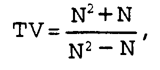
wobei N = 3,5,7,9,...
beschreiben. - Aufgabe der vorliegenden Erfindung ist es eine Schaltungsanordnung zur Erzeugung gerader Tastverhältnisse bei ungerader Verteilung eines symmetrischen Taktsignals anzugeben.
- Diese Aufgabe wird durch den kennzeichnenden Teil des Anspruchs 1 gelöst. Eine Weiterbildung ist Kennzeichen des Unteranspruchs.
- Prinzip der vorliegenden Erfindung ist es, der im allgemeinen längeren "Low"-Phase von z. B. zwei Taktdauern, bei einer Teilung durch 3, eine halbe Taktdauer, abzuziehen und der kürzeren "High"-Phase von z. B. einer Taktdauer, bei einer Teilung durch 3, eine halbe Taktdauer anzufügen.
- Hierzu dienen erste Mittel zur Erzeugung eines ersten Ausgangssignals aus dem symmetrischen Taktsignal. Dieses Ausgangssignal wird jeweils mit der n-ten Flanke von einem ersten Typ, z. B. der steigenden Flanke, des symmetrischen Taktsignals aktiv und bleibt dies für die Dauer von

Perioden des symmetrsichen Taktsignals. Zweite Mittel dienen zur Erzeugung eines zweiten Ausgangssignals aus dem symmetrischen Taktsignal, wobei dieses Ausgangssignal jeweils mit der n-ten Flanke vom anderen Typ, z. B. der fallenden, des symmetrischen Taktsignals aktiv wird und dies ebenfalls für die Dauer von
Perioden des symmetrischen Taktsignals bleibt. - Eine Logikanordnung verknüpft dann beide Ausgangssignale zu einem symmetrischen Ausgangssignal. Ist der aktive Zustand des ersten und zweiten Ausgangssignals jeweils "High", so kann die Logikanordnung aus einem ODER-Gatter bestehen bzw. aus einem UND-Gatter, wenn der aktive Zustand der Ausgangssignale "Low" ist.
- Die Erfindung wird nachfolgend anhand von zwei Figuren näher erläutert. Es zeigen:
- Figur 1
- ein Ausführungsbeispiel der erfindungsgemäßen Anordnung,
- Figur 2
- ein Zeitdiagramm verschiedener Signale der in Figur 1 gezeigten Schaltung.
- In Figur 1 ist eine erfindungsgemäße Ausführungsform eines symmetrischen Dreierteilers dargestellt. Mit 1 ist eine Eingangsklemme bezeichnet, an der das symmetrische Taktsignal zuführbar ist. Diese Eingangsklemme 1 ist jeweils mit dem Takteingang eines D-Latches 4 und 6 verbunden. Des weiteren ist sie über einen Inverter 2 mit dem Takteingang von jeweils einem weiteren D-Latches 3 und 5 verbunden. Der Ausgang Q des D-Latches 3 ist mit dem Eingang D des D-Latches 4 verschaltet. Ebenso ist der Ausgang Q des D-Latches 4 mit dem Eingang D des D-Latches 5 und der Ausgang Q des D-Latches 5 mit dem Eingang D des D-Latches 6 verbunden. Der Ausgang Q des D-Latches 5 ist mit dem ersten Eingang eines NOR-Gatters 7 verschaltet. Der zweite Eingang des NOR-Gatters 7 ist mit dem Ausgang Q des D-Latch 6 verbunden. Der Ausgang des NOR-Gatters 7 ist zum einen mit dem Eingang D des D-Latches 3 und zum anderen mit einer anderen Ausgangsklemme 8 verbunden. Die Buchstaben A, B, C, E bezeichnen Schaltungspunkte, an denen der in Figur 2 dargestellten Signalverläufe abgegriffen sind.
- Die in Figur 1 dargestellte Schaltung besteht aus einzelnen D-Latches, wobei zwei wiederum ein Master-Slave-Flip-Flop bilden. Die Verzögerung von einer halben Taktperiode läßt sich durch den Abgriff zwischen Master und Slave, d. h. zwischen den D-Latches 5, 6 erzeugen. Die in Figur 1 gezeigte Schaltung hat gleichzeitig den Vorteil, daß sie automatisch auf das feste interne Taktverhältnis


- Wie in Figur 2 zu sehen ist, wird am Ausgang B des D-Latches 5 ein Ausgangssignal erzeugt, das mit der fallenden Flanke des an der Eingangsklemme 1 anliegenden symmetrischen Taktsignals A aktiviert wird und für die Dauer einer Taktperiode aktiv bleibt. Dieses Signal wird im Abstand von drei Taktperioden generiert. Am Ausgang C des D-Latches 6 ist das gegenüber B erzeugte Ausgangssignal um eine halbe Taktperiode versetzt. Durch die NOR-Verknüpfung wird am Knoten D ein symmetrisches Ausgangssignal erzeugt. Dieses ist am Ausgang 8 abgreifbar.
Claims (2)
- Schaltungsanordnung zur Erzeugung gerader Tastverhältnis bei ungerader Teilung n eines symmetrischen Taktsignals, gekennzeichnet durch- erste Mittel zur Erzeugung eines ersten Ausgangssignals aus dem symmetrischen Taktsignal, das mit jeweils der n-ten Flanke vom ersten Typ des symmetrischen Taktsignals beginnt und für die Dauer von
 - zweite Mittel zur Erzeugung eines zweiten Ausgangssignals aus dem symmetrischen Taktsignal, das mit jeweils der n-ten Flanke vom anderen Typ des symmetrischen Taktsignals beginnt und für die Dauer von
 - einer Logikanordnung, die die beiden Ausgangssignale zu einem symmetrischen Ausgangssignal verknüpft.
 - Schaltungsanordnung nach Anspruch 1, dadurch gekennzeichnet, daß- n+1 in Reihe geschaltete D-Latches (3, 4, 5, 6) vorgesehen sind, die abwechselnd mit dem symmetrischen und dem invertierten symmetrischen Taktsignal getaktet werden,- die Ausgangssignale des letzten D-Latches (&) und des vorletzten D-Latches (5) einem NOR-Gatter (7) zugeführt werden,- das Ausgangssignal des NOR-Gatters (7) dem Eingang des ersten D-Latches (2) und einer Ausgangsklemme (8) zugeführt wird.
Applications Claiming Priority (2)
| Application Number | Priority Date | Filing Date | Title |
|---|---|---|---|
| DE4340966 | 1993-12-01 | ||
| DE4340966A DE4340966C1 (de) | 1993-12-01 | 1993-12-01 | Schaltungsanordnung zur Erzeugung gerader Tastverhältnisse |
Publications (3)
| Publication Number | Publication Date |
|---|---|
| EP0656691A2 true EP0656691A2 (de) | 1995-06-07 |
| EP0656691A3 EP0656691A3 (de) | 1996-03-13 |
| EP0656691B1 EP0656691B1 (de) | 1998-03-18 |
Family
ID=6503927
Family Applications (1)
| Application Number | Title | Priority Date | Filing Date |
|---|---|---|---|
| EP94118024A Expired - Lifetime EP0656691B1 (de) | 1993-12-01 | 1994-11-15 | Schaltungsanordnung zur Erzeugung eines symmetrischen Ausgangstaktsignals |
Country Status (3)
| Country | Link |
|---|---|
| US (1) | US5524037A (de) |
| EP (1) | EP0656691B1 (de) |
| DE (2) | DE4340966C1 (de) |
Families Citing this family (8)
| Publication number | Priority date | Publication date | Assignee | Title |
|---|---|---|---|---|
| EP0872959B1 (de) * | 1997-04-15 | 2003-12-10 | Koninklijke Philips Electronics N.V. | Rauscharmer Frequenzteiler |
| JP2002344308A (ja) * | 2001-05-18 | 2002-11-29 | Matsushita Electric Ind Co Ltd | 奇数分周器とそれを用いた90度移相器 |
| US20030092419A1 (en) * | 2001-11-09 | 2003-05-15 | Dan Nobbe | Method and apparatus for a near-unity divider in a direct conversion communication device |
| JP2003152530A (ja) * | 2001-11-13 | 2003-05-23 | Mitsubishi Electric Corp | 分周回路 |
| US6597212B1 (en) * | 2002-03-12 | 2003-07-22 | Neoaxiom Corporation | Divide-by-N differential phase interpolator |
| US6995589B2 (en) * | 2003-06-13 | 2006-02-07 | Via Technologies Inc. | Frequency divider for RF transceiver |
| KR100969864B1 (ko) | 2008-09-03 | 2010-07-15 | 한국과학기술원 | Cml 타입 d 플립-플롭 및 이를 이용한 주파수 홀수 분주기 |
| US8058901B2 (en) * | 2008-09-19 | 2011-11-15 | Qualcomm Incorporated | Latch structure, frequency divider, and methods for operating same |
Family Cites Families (9)
| Publication number | Priority date | Publication date | Assignee | Title |
|---|---|---|---|---|
| DE283024C (de) * | ||||
| US3902125A (en) * | 1974-06-18 | 1975-08-26 | Us Army | Symmetric output, digital by three counter |
| JPS59181831A (ja) * | 1983-03-31 | 1984-10-16 | Toshiba Corp | 可変分周器 |
| US4703495A (en) * | 1986-05-23 | 1987-10-27 | Advanced Micro Device, Inc. | High speed frequency divide-by-5 circuit |
| GB2198603A (en) * | 1986-12-05 | 1988-06-15 | Philips Electronic Associated | Divider circuit |
| DD283024A5 (de) * | 1989-05-03 | 1990-09-26 | Univ Dresden Tech | Schaltungsanordnung zur realisierung symmetrischer tastverhaeltnisse bei ungeradzahligen teilerverhaeltnissen |
| JP3003078B2 (ja) * | 1989-10-16 | 2000-01-24 | 日本無線株式会社 | 分周比の切換え可能な分周回路 |
| FI88837C (fi) * | 1991-08-15 | 1993-07-12 | Nokia Mobile Phones Ltd | Frekvensdividering med udda tal och decimaltal |
| JP2997139B2 (ja) * | 1992-12-03 | 2000-01-11 | 富士通株式会社 | 分周回路 |
-
1993
- 1993-12-01 DE DE4340966A patent/DE4340966C1/de not_active Expired - Fee Related
-
1994
- 1994-11-15 DE DE59405470T patent/DE59405470D1/de not_active Expired - Lifetime
- 1994-11-15 EP EP94118024A patent/EP0656691B1/de not_active Expired - Lifetime
- 1994-12-01 US US08/347,886 patent/US5524037A/en not_active Expired - Lifetime
Also Published As
| Publication number | Publication date |
|---|---|
| EP0656691B1 (de) | 1998-03-18 |
| US5524037A (en) | 1996-06-04 |
| EP0656691A3 (de) | 1996-03-13 |
| DE4340966C1 (de) | 1995-01-19 |
| DE59405470D1 (de) | 1998-04-23 |
Similar Documents
| Publication | Publication Date | Title |
|---|---|---|
| DE69410410T2 (de) | Taktsignalgenerator für eine Vielzahl nicht überlappender Taktsignale | |
| DE2654050C3 (de) | Taktsignalsteuersystem eines Mikrocomputersystems | |
| DE2510186A1 (de) | Steuerschaltung fuer einen wechselrichter | |
| DE2723707A1 (de) | Taktgeberschaltung | |
| DE69007688T2 (de) | Signalgenerator. | |
| DE69119782T2 (de) | Präzisions phasenschiebersystem | |
| DE69830870T2 (de) | Kombinatorische Verzögerungsschaltung für einen digitalen Frequenzvervielfacher | |
| EP0588112A1 (de) | Anordnung zur Taktrückgewinnung | |
| DE3850808T2 (de) | Erzeugung von Taktimpulsen. | |
| DE4340966C1 (de) | Schaltungsanordnung zur Erzeugung gerader Tastverhältnisse | |
| DE3130242A1 (de) | Elektronische steuerschaltung zur erzeugung eines monostabilen schaltverhaltens bei einem bistabilen relais | |
| DE1962455B2 (de) | Elektronischer frequenzumsetzer | |
| DE4433512C2 (de) | Wellenform-Formatierungseinrichtung | |
| DE4428545A1 (de) | Schaltungsanordnung zur Umwandlung eines seriellen Datensignals in ein paralleles Datensignal | |
| EP0042961B1 (de) | Verfahren und Anordnung zur Erzeugung von Impulsen vorgegebener Zeitrelation innerhalb vorgegebener Impulsintervalle mit hoher zeitlicher Auflösung | |
| DE3855895T2 (de) | Taktsignal-Versorgungssystem | |
| DE10004108C1 (de) | Schaltungsanordnung zur Generierung eines Ausgangs-Taktsignals mit optimierter Signalgenerierungszeit | |
| DE19963684B4 (de) | Verzögerungs-Verriegelungsschleifen-Taktgenerator, welcher Verzögerungs-Impuls-Verzögerungsumwandlung einsetzt | |
| CH661388A5 (de) | Digitale phasenschieberschaltung fuer einen thyristor-stromrichter. | |
| DE2401781C2 (de) | Anordnung zur Takterzeugung für ladungsgekoppelte Schaltungen | |
| DE2724110C2 (de) | Quasi-Zufallsgenerator | |
| EP0209189B1 (de) | Anordnung zur Synchronisation der pulsbreitenmodulierten Schalttakte mehrerer getakteter Gleichspannungswandler | |
| DE3142167A1 (de) | "teilerschaltung mit einstellbarem teilerverhaeltnis" | |
| EP0410212A2 (de) | Redundante Taktgeberanordnung | |
| EP0760567A2 (de) | Digitaler QAM-modulator |
Legal Events
| Date | Code | Title | Description |
|---|---|---|---|
| PUAI | Public reference made under article 153(3) epc to a published international application that has entered the european phase |
Free format text: ORIGINAL CODE: 0009012 |
|
| AK | Designated contracting states |
Kind code of ref document: A2 Designated state(s): DE FR GB IT |
|
| PUAL | Search report despatched |
Free format text: ORIGINAL CODE: 0009013 |
|
| AK | Designated contracting states |
Kind code of ref document: A3 Designated state(s): DE FR GB IT |
|
| 17P | Request for examination filed |
Effective date: 19960917 |
|
| 17Q | First examination report despatched |
Effective date: 19970317 |
|
| GRAG | Despatch of communication of intention to grant |
Free format text: ORIGINAL CODE: EPIDOS AGRA |
|
| GRAG | Despatch of communication of intention to grant |
Free format text: ORIGINAL CODE: EPIDOS AGRA |
|
| GRAH | Despatch of communication of intention to grant a patent |
Free format text: ORIGINAL CODE: EPIDOS IGRA |
|
| GRAH | Despatch of communication of intention to grant a patent |
Free format text: ORIGINAL CODE: EPIDOS IGRA |
|
| GRAA | (expected) grant |
Free format text: ORIGINAL CODE: 0009210 |
|
| AK | Designated contracting states |
Kind code of ref document: B1 Designated state(s): DE FR GB IT |
|
| REF | Corresponds to: |
Ref document number: 59405470 Country of ref document: DE Date of ref document: 19980423 |
|
| ET | Fr: translation filed | ||
| ITF | It: translation for a ep patent filed | ||
| GBT | Gb: translation of ep patent filed (gb section 77(6)(a)/1977) |
Effective date: 19980520 |
|
| PLBE | No opposition filed within time limit |
Free format text: ORIGINAL CODE: 0009261 |
|
| STAA | Information on the status of an ep patent application or granted ep patent |
Free format text: STATUS: NO OPPOSITION FILED WITHIN TIME LIMIT |
|
| 26N | No opposition filed | ||
| REG | Reference to a national code |
Ref country code: GB Ref legal event code: IF02 |
|
| PG25 | Lapsed in a contracting state [announced via postgrant information from national office to epo] |
Ref country code: IT Free format text: LAPSE BECAUSE OF NON-PAYMENT OF DUE FEES;WARNING: LAPSES OF ITALIAN PATENTS WITH EFFECTIVE DATE BEFORE 2007 MAY HAVE OCCURRED AT ANY TIME BEFORE 2007. THE CORRECT EFFECTIVE DATE MAY BE DIFFERENT FROM THE ONE RECORDED. Effective date: 20051115 |
|
| REG | Reference to a national code |
Ref country code: GB Ref legal event code: 732E Free format text: REGISTERED BETWEEN 20110707 AND 20110713 |
|
| REG | Reference to a national code |
Ref country code: FR Ref legal event code: TP Owner name: INFINEON TECHNOLOGIES AG, DE Effective date: 20110922 |
|
| REG | Reference to a national code |
Ref country code: DE Ref legal event code: R081 Ref document number: 59405470 Country of ref document: DE Owner name: INTEL MOBILE COMMUNICATIONS GMBH, DE Free format text: FORMER OWNER: SIEMENS AKTIENGESELLSCHAFT, 80333 MUENCHEN, DE Effective date: 20111107 Ref country code: DE Ref legal event code: R081 Ref document number: 59405470 Country of ref document: DE Owner name: INTEL MOBILE COMMUNICATIONS TECHNOLOGY GMBH, DE Free format text: FORMER OWNER: SIEMENS AKTIENGESELLSCHAFT, 80333 MUENCHEN, DE Effective date: 20111107 |
|
| REG | Reference to a national code |
Ref country code: FR Ref legal event code: TP Owner name: INTEL MOBILE COMMUNICATIONS GMBH, DE Effective date: 20120404 |
|
| REG | Reference to a national code |
Ref country code: GB Ref legal event code: 732E Free format text: REGISTERED BETWEEN 20121213 AND 20121219 |
|
| REG | Reference to a national code |
Ref country code: DE Ref legal event code: R081 Ref document number: 59405470 Country of ref document: DE Owner name: INTEL MOBILE COMMUNICATIONS GMBH, DE Free format text: FORMER OWNER: INFINEON TECHNOLOGIES AG, 85579 NEUBIBERG, DE Effective date: 20130315 Ref country code: DE Ref legal event code: R081 Ref document number: 59405470 Country of ref document: DE Owner name: INTEL MOBILE COMMUNICATIONS GMBH, DE Free format text: FORMER OWNER: INFINEON TECHNOLOGIES AG, 85579 NEUBIBERG, DE Effective date: 20130314 Ref country code: DE Ref legal event code: R081 Ref document number: 59405470 Country of ref document: DE Owner name: INTEL MOBILE COMMUNICATIONS GMBH, DE Free format text: FORMER OWNER: INTEL MOBILE COMMUNICATIONS TECHNOLOGY GMBH, 85579 NEUBIBERG, DE Effective date: 20130326 Ref country code: DE Ref legal event code: R081 Ref document number: 59405470 Country of ref document: DE Owner name: INTEL MOBILE COMMUNICATIONS GMBH, DE Free format text: FORMER OWNER: INTEL MOBILE COMMUNICATIONS GMBH, 85579 NEUBIBERG, DE Effective date: 20130315 |
|
| REG | Reference to a national code |
Ref country code: GB Ref legal event code: 732E Free format text: REGISTERED BETWEEN 20131017 AND 20131023 |
|
| PGFP | Annual fee paid to national office [announced via postgrant information from national office to epo] |
Ref country code: DE Payment date: 20131113 Year of fee payment: 20 Ref country code: GB Payment date: 20131113 Year of fee payment: 20 Ref country code: FR Payment date: 20131108 Year of fee payment: 20 |
|
| REG | Reference to a national code |
Ref country code: DE Ref legal event code: R071 Ref document number: 59405470 Country of ref document: DE |
|
| REG | Reference to a national code |
Ref country code: GB Ref legal event code: PE20 Expiry date: 20141114 |
|
| PG25 | Lapsed in a contracting state [announced via postgrant information from national office to epo] |
Ref country code: GB Free format text: LAPSE BECAUSE OF EXPIRATION OF PROTECTION Effective date: 20141114 |