EP0657928A1 - Nichtflüchtige Speicheranordnung - Google Patents
Nichtflüchtige Speicheranordnung Download PDFInfo
- Publication number
- EP0657928A1 EP0657928A1 EP94309254A EP94309254A EP0657928A1 EP 0657928 A1 EP0657928 A1 EP 0657928A1 EP 94309254 A EP94309254 A EP 94309254A EP 94309254 A EP94309254 A EP 94309254A EP 0657928 A1 EP0657928 A1 EP 0657928A1
- Authority
- EP
- European Patent Office
- Prior art keywords
- oxide
- polysilicon
- bit line
- dielectric
- substrate
- Prior art date
- Legal status (The legal status is an assumption and is not a legal conclusion. Google has not performed a legal analysis and makes no representation as to the accuracy of the status listed.)
- Granted
Links
- 229910021420 polycrystalline silicon Inorganic materials 0.000 claims abstract description 123
- 229920005591 polysilicon Polymers 0.000 claims abstract description 121
- 238000007667 floating Methods 0.000 claims abstract description 68
- 238000000034 method Methods 0.000 claims abstract description 41
- 238000009792 diffusion process Methods 0.000 claims abstract description 17
- 238000004519 manufacturing process Methods 0.000 claims abstract description 5
- 239000000758 substrate Substances 0.000 claims description 53
- 230000015654 memory Effects 0.000 claims description 28
- 150000004767 nitrides Chemical class 0.000 claims description 22
- 229920002120 photoresistant polymer Polymers 0.000 claims description 17
- 238000005530 etching Methods 0.000 claims description 11
- 229910052710 silicon Inorganic materials 0.000 claims description 10
- 239000010703 silicon Substances 0.000 claims description 10
- XUIMIQQOPSSXEZ-UHFFFAOYSA-N Silicon Chemical compound [Si] XUIMIQQOPSSXEZ-UHFFFAOYSA-N 0.000 claims description 9
- 238000000151 deposition Methods 0.000 claims description 9
- 239000012535 impurity Substances 0.000 claims description 9
- 238000010438 heat treatment Methods 0.000 claims description 6
- 238000001020 plasma etching Methods 0.000 claims description 5
- 230000000379 polymerizing effect Effects 0.000 claims description 3
- 239000004065 semiconductor Substances 0.000 claims description 2
- 239000002019 doping agent Substances 0.000 claims 1
- 230000008569 process Effects 0.000 abstract description 15
- 239000003989 dielectric material Substances 0.000 abstract description 12
- VYPSYNLAJGMNEJ-UHFFFAOYSA-N Silicium dioxide Chemical compound O=[Si]=O VYPSYNLAJGMNEJ-UHFFFAOYSA-N 0.000 abstract description 8
- 230000014759 maintenance of location Effects 0.000 abstract description 8
- 230000000694 effects Effects 0.000 abstract description 7
- 230000008878 coupling Effects 0.000 abstract description 6
- 238000010168 coupling process Methods 0.000 abstract description 6
- 238000005859 coupling reaction Methods 0.000 abstract description 6
- 229910052814 silicon oxide Inorganic materials 0.000 abstract description 4
- 238000012545 processing Methods 0.000 description 16
- 239000004020 conductor Substances 0.000 description 10
- 238000005516 engineering process Methods 0.000 description 9
- 230000003647 oxidation Effects 0.000 description 9
- 238000007254 oxidation reaction Methods 0.000 description 9
- 238000013461 design Methods 0.000 description 7
- 238000012986 modification Methods 0.000 description 7
- 230000004048 modification Effects 0.000 description 7
- 230000008901 benefit Effects 0.000 description 6
- 238000012876 topography Methods 0.000 description 5
- 229910052581 Si3N4 Inorganic materials 0.000 description 4
- 238000001465 metallisation Methods 0.000 description 4
- 101100521334 Mus musculus Prom1 gene Proteins 0.000 description 3
- QVGXLLKOCUKJST-UHFFFAOYSA-N atomic oxygen Chemical compound [O] QVGXLLKOCUKJST-UHFFFAOYSA-N 0.000 description 3
- 239000007943 implant Substances 0.000 description 3
- 239000001301 oxygen Substances 0.000 description 3
- 229910052760 oxygen Inorganic materials 0.000 description 3
- 230000027756 respiratory electron transport chain Effects 0.000 description 3
- HQVNEWCFYHHQES-UHFFFAOYSA-N silicon nitride Chemical compound N12[Si]34N5[Si]62N3[Si]51N64 HQVNEWCFYHHQES-UHFFFAOYSA-N 0.000 description 3
- 239000000126 substance Substances 0.000 description 3
- 230000005641 tunneling Effects 0.000 description 3
- 238000001039 wet etching Methods 0.000 description 3
- 238000009279 wet oxidation reaction Methods 0.000 description 3
- KRHYYFGTRYWZRS-UHFFFAOYSA-N Fluorane Chemical compound F KRHYYFGTRYWZRS-UHFFFAOYSA-N 0.000 description 2
- NBIIXXVUZAFLBC-UHFFFAOYSA-N Phosphoric acid Chemical compound OP(O)(O)=O NBIIXXVUZAFLBC-UHFFFAOYSA-N 0.000 description 2
- 238000003491 array Methods 0.000 description 2
- 229910052785 arsenic Inorganic materials 0.000 description 2
- -1 arsenic ions Chemical class 0.000 description 2
- 230000015572 biosynthetic process Effects 0.000 description 2
- 230000000903 blocking effect Effects 0.000 description 2
- 239000000969 carrier Substances 0.000 description 2
- 238000005229 chemical vapour deposition Methods 0.000 description 2
- 230000006870 function Effects 0.000 description 2
- 238000001459 lithography Methods 0.000 description 2
- 230000002093 peripheral effect Effects 0.000 description 2
- 230000000717 retained effect Effects 0.000 description 2
- 235000012239 silicon dioxide Nutrition 0.000 description 2
- 239000000377 silicon dioxide Substances 0.000 description 2
- 230000001154 acute effect Effects 0.000 description 1
- 229910000147 aluminium phosphate Inorganic materials 0.000 description 1
- 230000004888 barrier function Effects 0.000 description 1
- 230000015556 catabolic process Effects 0.000 description 1
- 238000007796 conventional method Methods 0.000 description 1
- 230000001351 cycling effect Effects 0.000 description 1
- 230000007423 decrease Effects 0.000 description 1
- 230000008021 deposition Effects 0.000 description 1
- 239000012895 dilution Substances 0.000 description 1
- 238000010790 dilution Methods 0.000 description 1
- 238000001312 dry etching Methods 0.000 description 1
- 229910000040 hydrogen fluoride Inorganic materials 0.000 description 1
- 238000002513 implantation Methods 0.000 description 1
- 238000004518 low pressure chemical vapour deposition Methods 0.000 description 1
- 229910052751 metal Inorganic materials 0.000 description 1
- 239000002184 metal Substances 0.000 description 1
- 230000001590 oxidative effect Effects 0.000 description 1
- 238000002161 passivation Methods 0.000 description 1
- 230000005855 radiation Effects 0.000 description 1
- 230000009467 reduction Effects 0.000 description 1
- 239000000243 solution Substances 0.000 description 1
- 238000003860 storage Methods 0.000 description 1
- 230000008719 thickening Effects 0.000 description 1
- XLYOFNOQVPJJNP-UHFFFAOYSA-N water Substances O XLYOFNOQVPJJNP-UHFFFAOYSA-N 0.000 description 1
Images


Classifications
-
- H—ELECTRICITY
- H10—SEMICONDUCTOR DEVICES; ELECTRIC SOLID-STATE DEVICES NOT OTHERWISE PROVIDED FOR
- H10B—ELECTRONIC MEMORY DEVICES
- H10B69/00—Erasable-and-programmable ROM [EPROM] devices not provided for in groups H10B41/00 - H10B63/00, e.g. ultraviolet erasable-and-programmable ROM [UVEPROM] devices
-
- H—ELECTRICITY
- H10—SEMICONDUCTOR DEVICES; ELECTRIC SOLID-STATE DEVICES NOT OTHERWISE PROVIDED FOR
- H10B—ELECTRONIC MEMORY DEVICES
- H10B41/00—Electrically erasable-and-programmable ROM [EEPROM] devices comprising floating gates
- H10B41/30—Electrically erasable-and-programmable ROM [EEPROM] devices comprising floating gates characterised by the memory core region
Definitions
- This invention relates to integrated circuits and more particularly to a virtual ground non-volatile memory array with self-aligned interpoly dielectrics and method for manufacturing same.
- Non-volatile memory can be formed in either bipolar or MOS technology.
- MOS PROMs can be formed using one of three currently available technologies (EPROM, EEPROM or FLASH EPROM).
- Non-volatile MOS PROMs are designed and perform in numerous similar ways, and can be achieved using many well-known technologies such as: (i) floating gate tunnel oxide, (ii) textured poly, (iii) metal nitride oxide silicon (MNOS), and (iv) EPROM - tunnel oxide (ETOX).
- Program and erase of the corresponding EPROM cell differs depending upon which technology is used. For example, a floating gate tunnel oxide EPROM transistor is programmed (moving electrons into the floating gate) by biasing the control gate, while erasure (moving electrons out of the floating gate) is achieved by biasing the drain.
- a textured poly-type EPROM device is achieved by electrons tunneling from a first polysilicon to a second polysilicon, wherein erase is achieved by electrons tunneling from the second polysilicon to a third polysilicon.
- MNOS-type devices allow charge to be stored in discrete traps in the bulk of the nitride.
- stacked polysilicon conductors be used to perform the program and erase function.
- a comparison on floating gate tunnel oxide, textured poly, MNOS technologies and the program and erase thereof is described by S. Lai et al., "Comparison and Trends in Today's Dominate E2 Technologies", Int'l Electron Devices Meeting Tech. Digest, (1986) pp. 580-583 (herein incorporated by reference).
- the stacked polysilicon conductors In order to form the stacked polysilicon conductors (one being a floating gate conductor and the other being a control gate conductor) numerous processing steps are required. Placement of the tunneling oxide, the floating gate and the dielectric between the floating gate and the control gate must be carefully performed such that each structure is aligned during the lithography steps. It is also essential that the floating gate, control gate, tunnel oxide and interpoly dielectric be of small critical dimensions and placed close to one another in order to provide a dense array of programmable transistors coupled to corresponding word and bit lines extending throughout the array.
- Array 10 includes a plurality of programmable transistors, each transistor having a channel region 12 placed below a stacked pair of control and floating gates 14 and 16.
- Control gate 14 is an elongated polysilicon strip placed a spaced distance (spaced by a dielectric) over floating gate 16.
- Field oxide 18 dielectrically isolates transistors from one another, and are etched or removed within the source regions 20 at edge 22 of polysilicon 14 by the well-known self-aligning process described above.
- Metalization layers (not shown) can be placed into contact windows 24 for making contact to drain regions 26, in order to form bit line conductors of the array.
- the EPROM array shown in Fig. 1 requires numerous contacts 24 be placed within the array. Geometry necessary to accommodate contacts forces an array area which can be quite large for multimegabit memories. In an effort to reduce array size for large memories, a higher density configuration has recently been advanced, as shown in Fig. 2.
- the array of Fig. 2 does not require contacts be placed within the array. If a transistor is selected, one side of the transistor channel is designated by the decode circuitry as either a ground or a bit line. As such, the contactless array of Fig. 2 is often referred to as "virtual ground" array.
- Virtual ground arrays generally utilize control polysilicon strips 28 be placed perpendicular to and a spaced distance over floating polysilicon strips 30.
- Control polysilicon 28 is coupled to a word line, and bit lines are formed between laterally spaced floating polysilicon 30 (i.e., within the drain area, on one side of channel 32).
- Channel 32 often called a gate region, is formed within the substrate beneath floating polysilicon 30.
- Channel 32 is controlled by the overlying polysilicon 28.
- Source (or drain) regions are formed on opposite sides of channel 32 or floating polysilicon 30. If one side of floating gate 30 is designed as the drain, the other side can be designated as a grounded source.
- the drain extends as a contiguous diffusion region beneath a field oxide and between pairs of adjacent floating gates. The entire contiguous diffusion area or drain can then be accessed via a contact placed near the periphery of the array 34.
- bit line diffusion areas 36 drain or source areas
- bit line oxides are buried within the substrate and beneath a bit line oxide, as will be described below. Formation of buried bit line diffusions, overlying bit line oxides and interpoly dielectrics, all require careful attention be paid to the lithography process. Any mis-alignment or mis-processing could have serious consequences in the operation of the array. A single inoperable transistor could cause an ensuing part to fail. Thus, it is important that when processing a virtual ground array careful attention must be paid to each processing step.
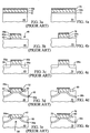
- Figs. 3a-3h cross-sectional views taken during various processing steps of a single programmable transistor along plane A-A of Fig. 2 are shown.
- a silicon substrate 40 Placed on the upper surface of a silicon substrate 40 is a first gate oxide 42.
- Gate oxide 42 often referred to as “tunnel oxide” allows electron transfer from the source or drain region to an overlying floating polysilicon 30a.
- a description of electron transfer through tunnel oxide, based upon well-known EPROM-tunnel oxide (ETOX) technology is provided by K. Robinson, "Endurance Brightens the Future of Flash -- Memory as a Viable Mask-Storage Alternative," Electronic Design News , (November 1988) pp. 167-169 (herein incorporated by reference).
- Dielectric 46a Placed on the upper surface of floating polysilicon 30a, is an interpoly dielectric 46a.
- Dielectric 46a is preferably a trilayer structure comprising oxide-nitride-oxide layering.
- the bottom layer of the trilayer structure is a thermally grown oxide (thermally grown from polysilicon 30a feed stock) similar to thermally grown oxide 42.
- the bottom layer of the trilayer structure is approximately 120 angstroms ( ⁇ ) in thickness.
- a nitride is then deposited over the bottom oxide layer using conventional chemical vapor deposition (CVD) techniques to, e.g., a thickness of approximately 190 ⁇ , and the overlying oxide grown upon the nitride is, e.g., generally 40 ⁇ in thickness.
- CVD chemical vapor deposition
- a trilayer dielectric is advantageous in that (i) it provides good data retention characteristics, (ii) it is fairly thin in order to achieve good coupling between control and floating polysilicon, and (iii) the nitride prevents oxide thickening in subsequent oxidation steps.
- the nitride layer can be formed in a low pressure CVD chamber, whereas the bottom oxide of the trilayer structure (polysilicon oxide) is grown by a low-temperature dry oxidation process.
- the upper oxide (nitride oxide) can be formed by high-temperature wet oxidation.
- oxide-nitride-oxide (ONO) interpoly dielectrics within virtual ground PROM architectures is described by Y.
- first gate oxide 42, floating polysilicon 30a and interpoly dielectric 46a have been placed across substrate 40 within the core area, photoresist is deposited across the top of the substrate topography and select regions of the photoresist are exposed to radiation. Depending upon whether the photoresist is positive or negative, various areas of the photoresist will be polymerized in accordance with the mask pattern placed proximate to the photoresist. The polymerized photoresist is retained while the unpolymerized photoresist is removed thereby providing etched windows to the underlying substrate topography. As shown in Fig. 3b, select regions of oxide 42, polysilicon 30a, and dielectric 46a are removed in accordance with the patterned photoresist.
- Etched areas 48 are thereafter adapted to receive implant of impurities necessary to form bit line diffusion areas 36a shown in Fig. 3c.
- bit line areas 36a are doped using arsenic ions.
- the arsenic ions implant within the opposite polarity substrate 40 to form conductive regions therein, according to well-known source/drain implant techniques.
- bit line oxide 50 is thermally grown at the silicon-oxide interface 52, as shown in Fig. 3d.
- oxide grows on many feed stock substances such as silicon and polycrystalline silicon (polysilicon).
- Oxide 50 grows at a faster rate upon the silicon substrate 40 than upon the side wall of polysilicon 30a, as evidenced by the illustration of Fig. 3d.
- oxide 50 can be grown in a dry oxygen ambient since dry oxide is less porous than wet oxide. As such, dry oxide generally grows at a slower rate than wet oxide, provided all other conditions are equal. However, the dry oxide exhibits a lesser tendency to allow carriers to pass through the less porous substance. Accordingly, dry oxide achieves better data retention by minimizing inadvertent Fowler-Nordheim emissions.
- dielectric 46a An important aspect of dielectric 46a is the ability of Si3N4 to minimize growth of oxide upon the dielectric. Nitride is a well-known substance which does not accept a substantial amount of oxide growth thereon. Accordingly, oxide growth is limited to the bit line areas 36a and the sides of the polycrystalline silicon 30a. Minimum growth at the upper surface of polysilicon 30a ensures a thin dielectric 46a and, as a result, provides strong coupling between polysilicon 30a and any overlying conductor placed upon the dielectric.
- thermally grown oxide 50 An inherent problem with thermally grown oxide 50 is the need for raising the temperature of the substrate during the growth process. Generally speaking, dry oxidation occurs at a slower rate than wet oxidation. In order to enhance the dry oxidation process, the temperature of the substrate is oftentimes raised to a level between 800°C to 1100°C. Thermally cycling the substrate 40 causes bit line areas 36a to diffuse into and laterally along substrate 40. As shown in Fig. 3e, bit line areas 36a can extend into channel region 54 causing what is commonly known as "short channel effects". Short channel effects caused by shrinking effective gate lengths, leads to a reduction in threshold voltages of the associated device.
- Short channel effects can also cause subthreshold current through the channel (i.e., punchthrough current within the substrate bulk or drain-induced barrier lower (DIBL) current at or near the substrate surface.
- DIBL drain-induced barrier lower
- Punchthrough and DIBL-induced current occurs between the closely spaced bit line areas when subthreshold voltages are applied to the gate, and normal voltage levels exist between the drain and source.
- Punchthrough and DIBL-induced current can lead to break-down voltage (BVDSS) problems, which is well documented and is particularly acute in short channel length transistors.
- BVDSS break-down voltage
- dielectric 46a is removed according to conventional techniques for removing oxide and silicon nitride.
- oxide silicon dioxide
- plasma etching includes reactive ion etching and its derivatives, whereby wet etching includes hydrogen fluoride (HF) in various dilutions in water.
- Silicon nitride can also be wet etched with either HF solutions or with hot phosphoric acid. The etching process is sufficiently selective in order to remove predominant amounts of dielectric 46a while retaining bit line oxide 50.
- dielectric 46a is only temporarily placed. Dielectric 46a is needed only to prevent oxygen diffusion to the upper surface of polysilicon 30a during times in which bit line oxide 50 is grown. Thereafter, dielectric 46a is removed in order to provide a more planer upper polysilicon surface for receiving a second interpoly dielectric 46b. Removing dielectric 46a and replacing it with another interpoly dielectric 46b, which extends around a substantial portion of three sides of floating polysilicon 30a, occurs in such a manner that dielectric 46a is often referred to as a "sacrificial dielectric". The problems inherent in removing sacrificial dielectrics are manyfold.
- the etching process necessary to remove a trilayer structure of oxide-nitride-oxide is fairly complex. Oftentimes, small areas of silicon nitride or silicon dioxide are left after they should have been removed. The residue associated with the wet or dry etching process can lead to non-planer upper surfaces. Secondly, removal of the trilayer structure may not be complete across the entire surface leading to a thicker than expected subsequent dielectric, which can lead to problems of lower than expected electrical coupling to the overlying control polysilicon. Thirdly, poor selectivity during the etching process can inadvertently remove bit line oxide 50 causing higher than expected electrical coupling between bit line areas 36a and overlying control polysilicon. It is therefore, important to try and minimize the number of processing steps and particularly to minimize or eliminate under and over etching of the sacrificial dielectric and areas surrounding the same.
- interpoly dielectric 46b is placed across the upper surface of floating polysilicon 30a and bit line oxides 50.
- Reintroduction of an ONO trilayer involves thermally growing corresponding oxides.
- a polysilicon/silicon oxide 56 (grown from, and part of, ONO 46b) is formed as a thin layer.
- substrate 40 is exposed to additional thermal cycles causing bit line areas 36a to further diffuse laterally and to a deeper depth within substrate 40. Lateral diffusion adds to the short channel effects described above, and deeper diffusions produce carrier mobility across channel regions thereby producing higher junction capacitance and a slower device.
- thermal cycles associated with substrate 40 cause mobile carriers within channel 54 to diffuse to a deeper depth thereby offsetting the advantages of shallow channel devices.
- Fig. 3g illustrates an oxide 56 grown at the interface region between the silicon (or polysilicon) and oxide 50.
- Oxide 56 is the polysilicon oxide normally associated with the ONO trilayer, and is incorporated prior to the introduction of second polysilicon 28a.
- a second gate oxide which must be grown for the peripheral transistors affects the core thermally, but has no effect on core oxides due to the blocking nitride of the ONO trilayer.
- Second polysilicon (or poly) 28 is placed in both the core (array) area as well as in periphery areas surrounding the array. Second poly 28 forms the gate conductors within the core regions of the EPROM as well as any logic necessary for operating the control/decode circuitry. Second poly 28 associated with the array area is often referred to as control polysilicon.
- Fig. 3h illustrates control (or second) polysilicon 28 placed on the upper surface of interpoly dielectric 46b to complete a stacked gate region illustrating cross-section along plane A-A of Fig. 2. It is well known that further processing is required to self-align etch the floating gates to the control gates. It is also well recognized that additional metalization layers can be formed in contact regions and upon a monolithic circuit embodying a virtual ground array 20 of conventional design. As such, metalization in contact regions is formed subsequent to the step shown in Fig. 3h in accordance with technology well-known to the skilled artisan.
- the problems outlined above are in large part solved by the virtual ground non-volatile memory to be described herein.
- the virtual ground memory comprises a self-aligned interpoly dielectric which is purposefully not a sacrificial interpoly dielectric.
- the present memory array avoids subjecting the surface topography to inaccurate etching processes, and also avoids subjecting the silicon substrate and bit line diffusions to undue thermal cycles. Accordingly, a more closely controlled dielectric thickness can be achieved between floating and control polysilicon.
- bit line oxides do not experience sacrificial etches of prior designs.
- the self-aligned dielectrics and memory circuits incorporating those dielectrics achieve higher performance and more consistent performance for each programmable transistor within the array.
- a non-volatile memory array comprising a semiconductor substrate and a first gate oxide placed upon the substrate.
- a plurality of floating polysilicon strips are spaced apart from each other and placed upon the first gate oxide to form a programmable region.
- a plurality of control polysilicon strips are spaced apart from each other and extend perpendicular to each of the floating polysilicon strips.
- a dielectric is patterned only in the cross-over regions directly between the floating polysilicon strips and the control polysilicon strips. The dielectric is aligned with the edges of the respective floating polysilicon strips and respective control polysilicon strips.
- a plurality of coplanar bit line oxides are formed beneath the control polysilicon strips and between the floating polysilicon strips.
- a plurality of diffusion regions are formed beneath respective bit line oxides.
- a set of the plurality of the diffusion regions form a conductive channel extending perpendicular to and between adjacent control polysilicon strips.
- the interpoly dielectric comprises polysilicon oxide, nitride, and nitride oxide placed in a trilayer structure.
- the edges of the floating polysilicon strips comprise wet oxide grown thereon followed by dry oxide grown at the wet oxide-polysilicon interface.
- the wet oxide is formed in a steam ambient and the dry oxide is formed in an O2 ambient.
- a plurality of diffusion regions forming a conductive channel extends across the memory array to a contact point adapted for receiving a ground voltage.
- the method comprises the steps of growing a first gate oxide upon a silicon substrate, and then depositing a floating polysilicon upon the first gate oxide.
- a dielectric is deposited upon the floating polysilicon, wherein portions of the floating polysilicon and dielectric are removed from a plurality of bit line areas spaced across the substrate.
- the bit line areas are then implanted with impurities, wherein the impurities reside at a specified depth within the substrate.
- a bit line oxide is then grown within the bit line areas at the oxide-silicon interface and above the implanted impurities.
- the dielectric is retained upon the upper surface of the floating polysilicon after the bit line oxide is grown, and thereafter, a second gate oxide is grown within the bit line areas.
- the step of removing floating polysilicon and dielectric from the bit line areas comprises the steps of placing photoresist upon the dielectric and polymerizing the photoresist in gate regions overlying channel areas within the substrate. Next, unpolymerized photoresist is removed to form windows above respective bit line areas such that portions of the dielectric and underlying floating polysilicon can be etched away.
- the step of growing the bit line oxide comprises pressurizing and heating a furnace to approximately 1-2 atmospheres and 900-950° C, respectively, and then placing the substrate into the furnace and passing steam across the substrate at a rate of approximately 1-8 slpm.
- the step of growing the second gate oxide comprises pressurizing and heating a furnace to approximately 1-2 atmospheres and 1000° C, respectively, and then placing the substrate into the furnace and passing O2 across the substrate at a rate of approximately 10 slpm.
- FIGs. 4a-4h cross-sectional views of various processes and steps of the present invention are shown along plane A-A of Fig. 2.
- the steps shown in Figs. 4a-4h are but a few steps necessary to introduce the present invention.
- Various modifications and changes may be made to the processing steps, and provided the modifications and changes produce substantially the same result and would be obvious to one skilled in the art, said modifications and changes fall within the spirit and scope of the claims set forth below.
- Well-known processing steps and device configurations not described in detail in the steps illustrated in Figs. 4a-4h, are purposely not shown in order not to unnecessarily obscure the present invention.
- Figs. 4a-4h describe a processing methodology for allowing an interpoly dielectric to be self-aligned with the edges of a floating polysilicon strip residing below the dielectric.
- This method and device formed therefrom eliminate the need for sacrificial dielectrics and the etching and thermal cycles associated therewith.
- the memory array is particularly suitable for use with non-volatile memory cells such as PROMs (i.e., EPROMs, FLASH EPROMs, and EEPROMs).
- PROMs i.e., EPROMs, FLASH EPROMs, and EEPROMs
- Figs. 4a-4c illustrate first gate oxide 72, floating polysilicon 30b and ONO interpoly dielectric 76 placed on the upper surface of substrate 70.
- Oxide 72, polysilicon 30b and dielectric 76 can be selectively removed in order to allow implantation of bit line areas 78.
- bit line oxide 80 results from the oxidation step.
- oxidation of bit line areas 78 to form bit line oxides 80 occur within a steam ambient.
- Bit line oxide 80 is therefore a wet oxide having the advantages of a higher oxidation rate at a lower oxidation temperature.
- Wet bit line oxide is formed by pressurizing the oxide furnace to approximately 1-2 atmospheres and at a temperature of approximately 900-950° C. Steam is passed across the substrate at a rate of approximately 1-8 slpm. By using steam at the above-defined parameters, a wet oxide thickness at the substrate surface of approximately 1300 ⁇ can be formed in approximately 20-40 minutes.
- the oxide be formed not only quickly but at minimal elevated temperature.
- dry oxides require a temperature 100° C higher than wet oxides.
- the temperature differential leads to additional drive in of the bit line area 78 and enhances problems of short channel effects.
- the patterned interpoly dielectric 76 is not removed and remains throughout the processing steps.
- dielectric 76 is not a sacrificial dielectric as in conventional designs, and therefore, does not require additional etching steps be taken which could cause under etch or over etch of substrate topography. Wet etch or plasma etch techniques are not needed, and the problems which might be associated with those techniques are avoided.
- Fig. 4f illustrates floating polysilicon 74 surrounded by wet bit line oxide 80 and ONO dielectric 76 in order to achieve good data retention of a "programmed" voltage upon floating polysilicon 30b.
- polysilicon 30b retains the programmed voltage resulting from electron transfer from the programmable drain area bit line through first oxide 72 (tunnel oxide).
- first oxide 72 tunnel oxide
- the charge remains within floating polysilicon 30b for a long period of time due in part to the larger thickness achieved by wet oxide at the side walls and the ONO at the top of polysilicon 30b.
- wet oxide by itself cannot retain the charge long enough to be commercially viable in the application herein specified.
- Interpoly dielectric 76 is relatively thin, comprising a bottom layer polysilicon oxide of approximately 120 ⁇ , a nitride of approximately 190 ⁇ and an overlying nitride-oxide of approximately 40 ⁇ .
- the thin trilayer structure provides good coupling between floating polysilicon 30b and an overlying conductor, such as a control conductor described below.
- the nitride within the ONO structure prevents additional oxide growth at the upper surface of floating polysilicon 30b and between the stacked polysilicon members. Additional oxide generally occurs during a time in which a second gate oxide 82 is formed to achieve periphery transistors (transistors outside of the non-volatile array).
- Second gate oxide 82 is a dry oxide, wherein oxide 82 is formed by placing substrate 70 into a furnace pressurized at approximately 1-2 atmospheres and heated to approximately 1000° C. Dry oxygen or O2 is passed across the substrate at a rate of approximately 10 slpm. Dry oxide is well-known to be less porous than wet oxide. The dry oxide forms at a slower rate than wet oxide, unless it is subjected to a higher temperature. The temperature and parameters defined above allow dry oxide of approximately 200-300 ⁇ in thickness to grow at the interface region between polysilicon 30b/substrate 70 and bit line oxide 80. Dry oxide 82 enhances the integrity of the thicker wet oxide 80 by filling porous gaps within the wet oxide at the interface region.
- dry oxide formation decreases electron mobility within the resulting oxide structure and thereby further enhances data retention of programmed voltage upon polysilicon 30b. It is important to note that wet oxidation by itself yields poor data retention. Dry oxide of 120 ⁇ grown from the polysilicon improves data retention, but it is still substandard. Dry oxide of 200-300 ⁇ grown from polysilicon 30b fills all gaps in the wet oxide, thereby solving the data retention problem. Note that both the prior art process and the present process subject the device to this thermal cycle, which is necessary to form the gate oxide for peripheral transistors. However, the prior art process can receive no oxidizing benefit due to its blocking, wrap-around ONO trilayer.
- control polysilicon 28b is well-known in design and function as being the conductive polysilicon which forms word lines within the array and enables programmability (reading from and writing to) of select transistors within the array.
- non-volatile memory device such as, for example, an ETOX double poly FLASH EPROM device
- control and floating polysilicon as well as each bit line diffusion to respective conductors and/or decode circuitry arranged near the periphery of the EPROM array.
- This may require deposition of contact windows and additional metalization layers as well as passivation to the upper topography according to well-known MOS processing techniques.
- well-known processing steps which proceed or are subsequent to those taught in Figs.
Landscapes
- Non-Volatile Memory (AREA)
- Semiconductor Memories (AREA)
Applications Claiming Priority (2)
| Application Number | Priority Date | Filing Date | Title |
|---|---|---|---|
| US16540193A | 1993-12-10 | 1993-12-10 | |
| US165401 | 1993-12-10 |
Publications (2)
| Publication Number | Publication Date |
|---|---|
| EP0657928A1 true EP0657928A1 (de) | 1995-06-14 |
| EP0657928B1 EP0657928B1 (de) | 2002-02-27 |
Family
ID=22598761
Family Applications (1)
| Application Number | Title | Priority Date | Filing Date |
|---|---|---|---|
| EP94309254A Expired - Lifetime EP0657928B1 (de) | 1993-12-10 | 1994-12-12 | Nichtflüchtige Speicheranordnung |
Country Status (3)
| Country | Link |
|---|---|
| EP (1) | EP0657928B1 (de) |
| JP (1) | JPH07221210A (de) |
| DE (1) | DE69429975T2 (de) |
Cited By (1)
| Publication number | Priority date | Publication date | Assignee | Title |
|---|---|---|---|---|
| US8164955B2 (en) | 2007-08-14 | 2012-04-24 | Dongbu Hitek Co., Ltd. | NOR flash memory device and method for fabricating the same |
Families Citing this family (1)
| Publication number | Priority date | Publication date | Assignee | Title |
|---|---|---|---|---|
| KR100511032B1 (ko) * | 2003-02-28 | 2005-08-30 | 삼성전자주식회사 | 플로팅 게이트의 형성 방법 및 이를 이용한 불휘발성메모리 장치의 제조 방법 |
Citations (6)
| Publication number | Priority date | Publication date | Assignee | Title |
|---|---|---|---|---|
| EP0461764A2 (de) * | 1990-06-13 | 1991-12-18 | WaferScale Integration Inc. | EPROM-Matrix mit virtueller Erdung |
| EP0464432A2 (de) * | 1990-06-29 | 1992-01-08 | National Semiconductor Corporation | Asymmetrische EPROM-Zelle mit virtueller Erdung und Verfahren zur Herstellung |
| US5120671A (en) * | 1990-11-29 | 1992-06-09 | Intel Corporation | Process for self aligning a source region with a field oxide region and a polysilicon gate |
| US5151375A (en) * | 1990-06-13 | 1992-09-29 | Waferscale Integration, Inc. | EPROM virtual ground array |
| EP0552531A1 (de) * | 1992-01-22 | 1993-07-28 | Macronix International Co., Ltd. | Nichtflüchtige Speicherzelle und Anordnungsarchitektur |
| EP0573169A1 (de) * | 1992-06-02 | 1993-12-08 | National Semiconductor Corporation | Segmentweise löschbares FLASH-EPROM |
-
1994
- 1994-12-09 JP JP6306223A patent/JPH07221210A/ja active Pending
- 1994-12-12 DE DE69429975T patent/DE69429975T2/de not_active Expired - Lifetime
- 1994-12-12 EP EP94309254A patent/EP0657928B1/de not_active Expired - Lifetime
Patent Citations (6)
| Publication number | Priority date | Publication date | Assignee | Title |
|---|---|---|---|---|
| EP0461764A2 (de) * | 1990-06-13 | 1991-12-18 | WaferScale Integration Inc. | EPROM-Matrix mit virtueller Erdung |
| US5151375A (en) * | 1990-06-13 | 1992-09-29 | Waferscale Integration, Inc. | EPROM virtual ground array |
| EP0464432A2 (de) * | 1990-06-29 | 1992-01-08 | National Semiconductor Corporation | Asymmetrische EPROM-Zelle mit virtueller Erdung und Verfahren zur Herstellung |
| US5120671A (en) * | 1990-11-29 | 1992-06-09 | Intel Corporation | Process for self aligning a source region with a field oxide region and a polysilicon gate |
| EP0552531A1 (de) * | 1992-01-22 | 1993-07-28 | Macronix International Co., Ltd. | Nichtflüchtige Speicherzelle und Anordnungsarchitektur |
| EP0573169A1 (de) * | 1992-06-02 | 1993-12-08 | National Semiconductor Corporation | Segmentweise löschbares FLASH-EPROM |
Cited By (1)
| Publication number | Priority date | Publication date | Assignee | Title |
|---|---|---|---|---|
| US8164955B2 (en) | 2007-08-14 | 2012-04-24 | Dongbu Hitek Co., Ltd. | NOR flash memory device and method for fabricating the same |
Also Published As
| Publication number | Publication date |
|---|---|
| DE69429975T2 (de) | 2002-11-14 |
| JPH07221210A (ja) | 1995-08-18 |
| EP0657928B1 (de) | 2002-02-27 |
| DE69429975D1 (de) | 2002-04-04 |
Similar Documents
| Publication | Publication Date | Title |
|---|---|---|
| US5783457A (en) | Method of making a flash memory cell having an asymmetric source and drain pocket structure | |
| US4597060A (en) | EPROM array and method for fabricating | |
| US5595924A (en) | Technique of forming over an irregular surface a polysilicon layer with a smooth surface | |
| US5756385A (en) | Dense flash EEPROM cell array and peripheral supporting circuits formed in deposited field oxide with the use of spacers | |
| KR940006094B1 (ko) | 불휘발성 반도체 기억장치 및 그 제조방법 | |
| US6458656B1 (en) | Process for creating a flash memory cell using a photoresist flow operation | |
| US6252276B1 (en) | Non-volatile semiconductor memory device including assymetrically nitrogen doped gate oxide | |
| US6468864B1 (en) | Method of fabricating silicon nitride read only memory | |
| US6287917B1 (en) | Process for fabricating an MNOS flash memory device | |
| EP0388060A2 (de) | Dichte flash-EEPROM-Halbleiter-Speicheranordnung und Herstellungsverfahren | |
| US6538292B2 (en) | Twin bit cell flash memory device | |
| US20020146885A1 (en) | Method of fabricating a nitride read only memory cell | |
| US6399466B2 (en) | Method of manufacturing non-volatile semiconductor memory device storing charge in gate insulating layer therein | |
| US6420237B1 (en) | Method of manufacturing twin bit cell flash memory device | |
| US7183157B2 (en) | Nonvolatile memory devices | |
| US5457061A (en) | Method of making top floating-gate flash EEPROM structure | |
| KR20030014658A (ko) | 다양한 기술 및 애플리케이션에 대해 쉽게 수정가능한주변 트랜지스터를 갖는 셀프-얼라인 콘택 비휘발성메모리에 대한 구조 및 프로세스 | |
| US5264718A (en) | EEPROM cell array with tight erase distribution | |
| US6465303B1 (en) | Method of manufacturing spacer etch mask for silicon-oxide-nitride-oxide-silicon (SONOS) type nonvolatile memory | |
| US4713142A (en) | Method for fabricating EPROM array | |
| US6235582B1 (en) | Method for forming flash memory cell | |
| US20050164457A1 (en) | Non-volatile memory devices and methods of fabricating the same | |
| US6300194B1 (en) | Method for manufacturing semiconductor integrated electronic memory devices having a virtual ground cells matrix | |
| US6638822B2 (en) | Method for forming the self-aligned buried N+ type to diffusion process in ETOX flash cell | |
| US6277693B1 (en) | Self-aligned process for forming source line of ETOX flash memory |
Legal Events
| Date | Code | Title | Description |
|---|---|---|---|
| PUAI | Public reference made under article 153(3) epc to a published international application that has entered the european phase |
Free format text: ORIGINAL CODE: 0009012 |
|
| AK | Designated contracting states |
Kind code of ref document: A1 Designated state(s): BE DE DK ES FR GB GR IE IT LU NL PT SE |
|
| 17P | Request for examination filed |
Effective date: 19951121 |
|
| 17Q | First examination report despatched |
Effective date: 20000821 |
|
| GRAG | Despatch of communication of intention to grant |
Free format text: ORIGINAL CODE: EPIDOS AGRA |
|
| GRAG | Despatch of communication of intention to grant |
Free format text: ORIGINAL CODE: EPIDOS AGRA |
|
| GRAH | Despatch of communication of intention to grant a patent |
Free format text: ORIGINAL CODE: EPIDOS IGRA |
|
| GRAH | Despatch of communication of intention to grant a patent |
Free format text: ORIGINAL CODE: EPIDOS IGRA |
|
| REG | Reference to a national code |
Ref country code: GB Ref legal event code: IF02 |
|
| GRAA | (expected) grant |
Free format text: ORIGINAL CODE: 0009210 |
|
| AK | Designated contracting states |
Kind code of ref document: B1 Designated state(s): BE DE DK ES FR GB GR IE IT LU NL PT SE |
|
| PG25 | Lapsed in a contracting state [announced via postgrant information from national office to epo] |
Ref country code: NL Free format text: LAPSE BECAUSE OF FAILURE TO SUBMIT A TRANSLATION OF THE DESCRIPTION OR TO PAY THE FEE WITHIN THE PRESCRIBED TIME-LIMIT Effective date: 20020227 Ref country code: IT Free format text: LAPSE BECAUSE OF FAILURE TO SUBMIT A TRANSLATION OF THE DESCRIPTION OR TO PAY THE FEE WITHIN THE PRESCRIBED TIME-LIMIT;WARNING: LAPSES OF ITALIAN PATENTS WITH EFFECTIVE DATE BEFORE 2007 MAY HAVE OCCURRED AT ANY TIME BEFORE 2007. THE CORRECT EFFECTIVE DATE MAY BE DIFFERENT FROM THE ONE RECORDED. Effective date: 20020227 Ref country code: GR Free format text: LAPSE BECAUSE OF FAILURE TO SUBMIT A TRANSLATION OF THE DESCRIPTION OR TO PAY THE FEE WITHIN THE PRESCRIBED TIME-LIMIT Effective date: 20020227 Ref country code: BE Free format text: LAPSE BECAUSE OF FAILURE TO SUBMIT A TRANSLATION OF THE DESCRIPTION OR TO PAY THE FEE WITHIN THE PRESCRIBED TIME-LIMIT Effective date: 20020227 |
|
| REF | Corresponds to: |
Ref document number: 69429975 Country of ref document: DE Date of ref document: 20020404 |
|
| ET | Fr: translation filed | ||
| PG25 | Lapsed in a contracting state [announced via postgrant information from national office to epo] |
Ref country code: SE Free format text: LAPSE BECAUSE OF FAILURE TO SUBMIT A TRANSLATION OF THE DESCRIPTION OR TO PAY THE FEE WITHIN THE PRESCRIBED TIME-LIMIT Effective date: 20020527 Ref country code: PT Free format text: LAPSE BECAUSE OF FAILURE TO SUBMIT A TRANSLATION OF THE DESCRIPTION OR TO PAY THE FEE WITHIN THE PRESCRIBED TIME-LIMIT Effective date: 20020527 Ref country code: DK Free format text: LAPSE BECAUSE OF FAILURE TO SUBMIT A TRANSLATION OF THE DESCRIPTION OR TO PAY THE FEE WITHIN THE PRESCRIBED TIME-LIMIT Effective date: 20020527 |
|
| NLV1 | Nl: lapsed or annulled due to failure to fulfill the requirements of art. 29p and 29m of the patents act | ||
| PG25 | Lapsed in a contracting state [announced via postgrant information from national office to epo] |
Ref country code: ES Free format text: LAPSE BECAUSE OF FAILURE TO SUBMIT A TRANSLATION OF THE DESCRIPTION OR TO PAY THE FEE WITHIN THE PRESCRIBED TIME-LIMIT Effective date: 20020829 |
|
| PG25 | Lapsed in a contracting state [announced via postgrant information from national office to epo] |
Ref country code: LU Free format text: LAPSE BECAUSE OF NON-PAYMENT OF DUE FEES Effective date: 20021212 Ref country code: IE Free format text: LAPSE BECAUSE OF NON-PAYMENT OF DUE FEES Effective date: 20021212 |
|
| PLBE | No opposition filed within time limit |
Free format text: ORIGINAL CODE: 0009261 |
|
| STAA | Information on the status of an ep patent application or granted ep patent |
Free format text: STATUS: NO OPPOSITION FILED WITHIN TIME LIMIT |
|
| 26N | No opposition filed |
Effective date: 20021128 |
|
| REG | Reference to a national code |
Ref country code: IE Ref legal event code: MM4A |
|
| PGFP | Annual fee paid to national office [announced via postgrant information from national office to epo] |
Ref country code: GB Payment date: 20131211 Year of fee payment: 20 Ref country code: DE Payment date: 20131204 Year of fee payment: 20 |
|
| PGFP | Annual fee paid to national office [announced via postgrant information from national office to epo] |
Ref country code: FR Payment date: 20131209 Year of fee payment: 20 |
|
| REG | Reference to a national code |
Ref country code: DE Ref legal event code: R071 Ref document number: 69429975 Country of ref document: DE |
|
| REG | Reference to a national code |
Ref country code: GB Ref legal event code: PE20 Expiry date: 20141211 |
|
| PG25 | Lapsed in a contracting state [announced via postgrant information from national office to epo] |
Ref country code: GB Free format text: LAPSE BECAUSE OF EXPIRATION OF PROTECTION Effective date: 20141211 |