EP0657938B1 - Festkörperstrahlungsdetektortafel mit matrixförmig angeordneten, lichtempfindlichen Detektoren, so angeordnet, dass Kanteneffekte zwischen den Elementen minimiert werden - Google Patents
Festkörperstrahlungsdetektortafel mit matrixförmig angeordneten, lichtempfindlichen Detektoren, so angeordnet, dass Kanteneffekte zwischen den Elementen minimiert werden Download PDFInfo
- Publication number
- EP0657938B1 EP0657938B1 EP94119021A EP94119021A EP0657938B1 EP 0657938 B1 EP0657938 B1 EP 0657938B1 EP 94119021 A EP94119021 A EP 94119021A EP 94119021 A EP94119021 A EP 94119021A EP 0657938 B1 EP0657938 B1 EP 0657938B1
- Authority
- EP
- European Patent Office
- Prior art keywords
- modules
- radiation
- photosensitive detectors
- solid state
- photosensitive
- Prior art date
- Legal status (The legal status is an assumption and is not a legal conclusion. Google has not performed a legal analysis and makes no representation as to the accuracy of the status listed.)
- Expired - Lifetime
Links
Images


Classifications
-
- H—ELECTRICITY
- H10—SEMICONDUCTOR DEVICES; ELECTRIC SOLID-STATE DEVICES NOT OTHERWISE PROVIDED FOR
- H10F—INORGANIC SEMICONDUCTOR DEVICES SENSITIVE TO INFRARED RADIATION, LIGHT, ELECTROMAGNETIC RADIATION OF SHORTER WAVELENGTH OR CORPUSCULAR RADIATION
- H10F39/00—Integrated devices, or assemblies of multiple devices, comprising at least one element covered by group H10F30/00, e.g. radiation detectors comprising photodiode arrays
- H10F39/10—Integrated devices
- H10F39/12—Image sensors
-
- G—PHYSICS
- G01—MEASURING; TESTING
- G01T—MEASUREMENT OF NUCLEAR OR X-RADIATION
- G01T1/00—Measuring X-radiation, gamma radiation, corpuscular radiation, or cosmic radiation
- G01T1/16—Measuring radiation intensity
- G01T1/20—Measuring radiation intensity with scintillation detectors
- G01T1/2018—Scintillation-photodiode combinations
- G01T1/20182—Modular detectors, e.g. tiled scintillators or tiled photodiodes
-
- G—PHYSICS
- G01—MEASURING; TESTING
- G01T—MEASUREMENT OF NUCLEAR OR X-RADIATION
- G01T1/00—Measuring X-radiation, gamma radiation, corpuscular radiation, or cosmic radiation
- G01T1/16—Measuring radiation intensity
- G01T1/20—Measuring radiation intensity with scintillation detectors
- G01T1/2018—Scintillation-photodiode combinations
- G01T1/20184—Detector read-out circuitry, e.g. for clearing of traps, compensating for traps or compensating for direct hits
-
- G—PHYSICS
- G01—MEASURING; TESTING
- G01T—MEASUREMENT OF NUCLEAR OR X-RADIATION
- G01T1/00—Measuring X-radiation, gamma radiation, corpuscular radiation, or cosmic radiation
- G01T1/16—Measuring radiation intensity
- G01T1/20—Measuring radiation intensity with scintillation detectors
- G01T1/2018—Scintillation-photodiode combinations
- G01T1/20188—Auxiliary details, e.g. casings or cooling
- G01T1/2019—Shielding against direct hits
Definitions
- This invention relates generally to solid state radiation detection panels and, more particularly to large area solid state radiation detection panels constructed by adjoining a plurality of single unit sensor tiles, as basically known from WO-A-91/10921.
- X-rays are commonly used to diagnose medical conditions in humans and animals and in many industrial uses.
- an object typically a portion of the body of a person or animal, is exposed to X-rays while positioned in proximity of a radiation sensitive media.
- a latent image of the object is formed in the radiation sensitive media which can be subsequently developed to aid the medical practitioner in viewing aspects of the body which can not be directly visually seen.
- silver halide films in conjunction with a light emitting phosphor sensitive to X-rays are used for this purpose.
- Radiation detectors have been constructed which eliminate the use of silver halide films in the detection of the object subjected to X-ray radiation.
- Radiation detectors are designed to detect incident radiation and convert that incident radiation into an electrical signal which can be utilized to construct a pixel by pixel representation of the image.
- a radiation detector is sensitive to X-rays but instead of forming an image of the object in silver halide film, the radiation detector directly converts the energy contained in the X-rays to electrical signals. These electrical signals can then be digitized, if they aren't already digital, and can digitally represent the image of the exposed object in a pixel by pixel basis.
- the digital representation of the image can then be viewed on conventional displays or monitors, transmitted to remote sites, stored electronically and printed in imagers to provide a visual output similar to that which medical practitioner is accustomed.
- Such radiation detectors typically involve an array of photosensitive detector elements constructed in array to form an entire X-ray image.
- Typical X-ray images are 35.6 centimeters (14 inches) by 43.2 centimeters (17 inches) and typically comprise an array of pixels of approximately 4,000 X 5,000. Thus, as many as 20,000,000 pixels may be contained in a single image.
- a tiling approach has been used to construct large radiation detectors.
- a plurality, typically a large number, of individual radiation sensitive tiles are constructed, typically using integrated circuit technology.
- the tiles are relatively small and, thus, relatively easy to manufacture using conventional techniques.
- the individual tiles are then placed adjacent each to form a large radiation detector suitable for use with conventional X-ray machines.
- each individual tile has a surface onto which X-ray radiation is incident and since only a part of that surface of actually sensitive to X-ray radiation, the overall radiation detector has many "dead spots" or areas which are insensitive to the X-ray radiation.
- the large area sensor includes at least a first solid state sensor having an X-ray detector region and a blind non-detector border region. Positioned adjacent to the first sensor is a second solid state sensor having an X-ray detector region and a blind non-detector border region with respective non-detector regions being contiguous.
- a third solid state sensor having an X-ray detector region is positioned to overlie the first and second solid state sensors in such a way that the X-ray detector region of the third sensor overlies the blind non-detector regions of the first and second sensors, however, the third sensor also incorporates a blind non-detecting region.
- the alignment of the third solid state sensor is very critical and difficult to accomplish.
- the placement of the third solid state sensor on top of the first and second sensors results in a non-uniform surface. This non-uniformity can cause scattering of the X-rays leading to loss in resolution.
- the radiation sensitive area is contained at the center and is surrounded by the radiation non-sensitive area which is utilized for the addressing, read-out and metal contacts, thus leading to inevitable loss of information in the conventional large area sensors.
- WO-A-91/10921 corresponding to the preamble of claim 1, discloses an x-ray imaging system and solid state detector therefor having a plurality of closely adjacent radiation sensing arrays facing a plurality of preprocessing circuits. Bump bonds are connected directly from the sensing arrays to the preprocessing circuits. Added absorber material may be included next to the sensing arrays for converting impinging x-rays to free electrons for affecting a charge on the sensing arrays. Alternatively, a scintillator may be positioned between the sensing arrays and the preprocessing circuits and sensing cells in the sensing arrays may be exposed to the scintillator.
- WO-A-93/04384 discloses an x-ray imaging system and solid state detector having a scintillator for converting impinging x-rays into visible light.
- a sensor array has two opposed surfaces with a plurality of detectors at one of the surfaces and having the other of the surfaces facing the scintillator.
- a plurality of processing circuits facing the one surface are connected to the detectors by bump bonds.
- the radiation detection panel according to the invention has a plurality of modules positioned immediately adjacent each other.
- Each of the plurality of modules has an array of photosensitive detectors arranged in a plurality of rows and columns with each of the photosensitive detectors having a radiation sensitive area.
- Each of the plurality of modules also has an addressing circuit for selectively addressing one of the photosensitive detectors by addressing one of the plurality of rows and one of the plurality of columns and reading the output of the one of the array of photosensitive detectors.
- Each of the plurality of modules is arranged in a three dimensional structure in which the array of photosensitive detectors is arranged on a planar first surface of the module covering substantially the entire area of the planar first surface.
- the addressing circuit is located within the module in an area away from the planar first surface opposite from the received radiation. In this way, the radiation detection panel has a nearly contiguous radiation sensitive area over the first surface of the solid state radiation detection panel.
- the solid state radiation detection panel adapted to receive radiation on a first surface.
- the solid state radiation detection panel has a common substrate, preferably glass, a plurality of modules each of which has an array of photosensitive detectors arranged in a plurality of rows and a plurality of columns.
- Each of the photosensitive detectors has a radiation sensitive area and produces an output.
- An addressing and reading circuit selectively addresses one of the photosensitive detectors by addressing one of the plurality of rows and one of the plurality of columns and reads the output of the one of the array of photosensitive detectors.
- Each of the plurality of modules is arranged in a three dimensional structure in which the array of photosensitive detectors on the first surface covers substantially the entire area of the first surface and in which the addressing and reading circuit is located within the module in an area away from the first surface opposite from the received radiation.
- the plurality of modules of the solid state radiation detection panel are positioned immediately adjacent each other resulting in a near contiguous radiation sensitive area over the entire surface of the solid state radiation detection panel receiving the radiation.
- Panel addressing means for selectively addressing one of the photosensitive detectors in each of the plurality of modules by addressing the circuit within each of the plurality of modules.
- a panel reading means selectively reads the output of the one of the array of photosensitive detectors in each of the modules.
- An interconnection is positioned between the plurality of modules and the common substrate connecting the addressing and reading circuit of each of the plurality of modules to the panel addressing means and to the panel reading means, respectively.
- each of the plurality of modules has an array of photosensitive detectors, each representing a pixel, arranged on a first surface of the module in a plurality of rows and columns covering substantially the first surface.
- the photosensitive detectors located along an edge of the module are designated edge photosensitive detectors and the photosensitive detectors located interior of the module are designated inside photosensitive detectors.
- Each of the photosensitive detectors has a radiation sensitive area and non-radiation sensitive circuitry associated with one of the photosensitive detectors.
- Each of the edge photosensitive detectors has the non-radiation sensitive circuitry located along an edge which, with respect to the radiation sensitive area, is opposite from the edge of the module.
- the radiation sensitive area of the edge photosensitive detectors are smaller than the radiation sensitive area of the inside photosensitive detectors and wherein a distance from center to center of the radiation sensitive area of adjacent photosensitive detectors is maintained substantially constant between adjacent edge photosensitive detectors as adjacent inside photosensitive detectors.
- the module further has a p/n diode along the edge of the module.
- a layer of phosphor be positioned between the radiation sensitive area of the modules and the received radiation.
- a radiation detection panel 10 is illustrated in Figure 1.
- Individual photosensitive modules 12 are arranged in a plurality of rows and columns and are mounted on a flat substrate 14, such as a glass plate. Each individual module, or tile, 12 is responsive to incident radiation from the top as illustrated in Figure 1.
- On top of the photosensitive modules 12 is a layer of phosphor 16. Covering the top of radiation detection panel 10 is a protective front plate 18 which protects the underlying phosphor layer 16 and photosensitive tiles 12 with a hermetic seal 20.
- Below substrate 14 is an optional lead separator 22 designed to protect underlying electronic components from radiation exposure.
- Below separator 22 and opposite from the side of incident radiation is a printed wiring board 24 containing appropriate electronic components 26 associated with radiation detection panel 10.
- Flexible cable 28 provides an electrical connection between electrical contacts on the common substrate 14 connecting to electrical components within each tile 12 and electronic components 26 mounted on printed wiring board 24 opposite separator 22.
- X-ray radiation (after being modulated according to the object being imaged) is incident on the top surface (the surface containing front plate 18).
- the radiation passes through front plate 18 and strikes the layer of phosphor 16 which operates as a scintillation material converting the X-ray radiation into visible light.
- Visible light emitted by the phosphor 16 is detected by an array of photosensitive detectors in each of tiles 12.
- the photosensitive detectors convert the visible radiation into an electrical signal which may be read-out to associated electronic circuits.
- the value, typically digital, of the electronic signals then represents an imagewise pattern of the object being imaged.
- each tile 12 In addition to the photosensitive detectors in each tile 12, other peripheral circuitry is used to address and read-out the charge held by individual photosensitive detectors. Within each photosensitive detector there are three TFT (thin film transistors) switches, one for each of the x and y directions and one for read-out purposes.
- TFT thin film transistors
- each tile 12 consists of silicon photodiodes and thin film transistor (TFT) devices formed on silicon wafers, with a dimension of 5.4 centimeters x 5.4 centimeters (2.125 inches x 2.125 inches). Silicon photodiodes provide the individual photosensitive elements.
- each tile 12 contains a 624 by 624 array of, or 389,376, photosensitive detectors.
- the addressing and read-out circuitry is distributed within each sensor tile 12 with the interconnection lines for clocks (30, 31, 32 and 33), V out (34, 36), V dd (38), reset (40) and ground (41) exposed on the top as illustrated in Figure 2.
- a p + implantation and implantation annealing at 850° Centigrade is done to form a built-in field to drive the carriers away from the surface and to enhance blue light efficiency.
- Aluminum patterns are then conventionally formed using microlithography.
- the tiles 12 are then mounted on a phosphor 16. After proper alignment is achieved, the tiles 12 are held in place by a vacuum system and the edges surrounding the tiles 12 is trimmed away.
- a common substrate 14 is prepared with large metal tracks, with typical track widths in the range of 300 - 700 microns.
- the patterned common substrate 14 is then placed on top of the array of tiles 12 and a solder bump operation is performed to connect the metal pads in the tiles 12 to the metal tracks on the common substrate 14.
- the phosphor may be coated on a separate sheet or glass substrate and then glued to the array of sensor tiles 12. Alternatively, the entire array of tiles 12 may be coated with phosphor 16.
- the phosphor 16 may consist of conventional phosphors or pre-structured phosphors, such as gadolinium oxide sulfide doped with terbium or europium or other phosphors known to those skilled in the art.
- Another alternative phosphor 16 is an alkali halide which can be deposited directly on the sensor tiles 12, using the thin film deposition techniques known in the art.
- a non-inclusive representative alkali halide phosphor is thallium doped cesium iodide.
- FIG. 3 A cross sectional view of the tiling method for two tiles 12 is illustrated in Figure 3.
- the array of sensor tiles 12 is mounted on a glass plate 14 which is separated from the printed wiring board 24 by a lead plate 22.
- the lead plate 22 has a typical thickness of 1 millimeter.
- the lead plate 22 is used to protect the surface mount technology (SMT) devices 26 on the printed wiring board 24 from the possible damage caused by X-ray radiation.
- SMT surface mount technology
- the top of the array of sensor tiles 12 are then covered with a front plate 18 and hermetically sealed to keep the array of sensor tiles 12 in an inert gas.
- a cabling system 28 interconnects the electrical contacts on the common substrate 14 connecting to the components within each tile 12 to the SMT devices 26.
- this tiling approach is primarily designed for a large area direct digital read-out sensor, the approach can also be applicable to any sensors where large area is a requirement.
- One example is a high speed, high quality liquid crystal display.
- a p - epi layer is grown to a thickness of 10-15 microns on a p + type 10.24 cm (4 inches) diameter single crystal silicon wafer, followed by implantation of N well regions and dopants.
- the NMOS devices are implanted at the peripherals with p field regions to protect the devices from radiation.
- gate polysilicon is deposited as an amorphous silicon stage with POCl 3 followed by annealing to form polysilicon.
- N + type is implanted to form the source/drain regions, followed by the deposition of 1,000 to 2,000 Angstroms of silicon oxide as a gate oxide and deposition of Boron Phosphor Silicate Glass (BPSG) at a thickness of 8,000 Angstroms.
- BPSG Boron Phosphor Silicate Glass
- Aluminum is deposited at a thickness of 12,000 Angstroms to form the horizontal signal lines, peripheral interconnections, etc.
- An inter-level dielectric layer of Boron Silicate Glass is deposited at a thickness of 10,000 Angstroms and then etched to form vias. Aluminum is then deposited at a thickness of 8,000 Angstroms to form the vertical lines, interconnections, etc.
- a final scratch protection layer composed of an oxide plus nitride layer is deposited, followed by opening of the pad areas.
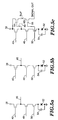
- Photosensitive module, tile, 12 consists of a 624 by 624 array of photosensitive detectors 42.
- a photo-diode 52 is sensitive to the radiation produced by the phosphor 16.
- a charge is stored in capacitor 54 based on the intensity of the light generated by the phosphor 16.
- the entire array is subdivided into eight sub-arrays 44 of 624 pixels by 78 pixels.
- the read-out line 46 of all photosensitive detectors 42 in each sub-array 44 is connected together.
- Each individual photosensitive detectors 42 within each sub-array 44 is individually sequentially addressed by shift clock registers (not shown). By subdividing the entire array in eight sub-arrays 44, eight pixels can be read-out of each tile simultaneously.
- a shift clock register increments by one, so that the next signal that comes in to the x address line 48 or y address line 50 will activate the next pixel in line.
- the pixels activated for reading are "marched down the line".
- the associated addressing and read-out circuitry may be located inside a tile 12 and away from the edges of each tile 12. Such read-out circuitry, beyond that shown in Figure 4 can be located on printed wiring board 24 on the opposite side of radiation detection panel 10 from the incident radiation.
- each read-out line 46 shown in Figure 4 and a metal track 60 is a solder bump 62. Since the number of metal tracks 60 on the substrate 14 is small, the size of the solder bumps 62 can be quite large (100-700 microns or more). The amount of real estate available in the substrate 14 is large compared with that available in conventional prior art systems which cram 624 x address lines and 624 y address lines into the same area.
- solder bumps 62 can be used for each line (metal track 60) contacted with the glass plate 14. In this way, solder bumps 62 can also help provide mechanical support.
- reset 40 Before exposure to X-ray radiation, reset 40 is set to a high level, preferably five volts.
- the x address line 48 and y address line 50 switches their associated thin film transistor (TFT) switches by applying a high voltage.
- a voltage is applied across photo-diode 52 for that pixel, to charge the photo-diode to the "full well” potential.
- "Full well” potential is 40 me - for a 85 x 85 micron pixel.
- reset 40 remains high.
- the x address line 48 and y address line 50 switches their associated TFT off (low voltage) after the exposure has started. By doing this, the photodiode and capacitor are isolated and the "full well” potential starts for “leak out” and reduces the potential across capacitor 54 in proportion to the light intensity from the phosphor 16.
- Read-out is illustrated by reference to Figure 5C.
- Reset 40 is still high at five volts.
- the x address line 48 and y address line 50 are still low.
- reset 40 is set to low and the x address line 48 and y address line 50 are set to high.
- the potential across capacitor 54 travels through "source follower” 64 with a gain of one.
- the "read out” TFT 66 is turned on to permit the signal to pass to "signal out", which goes through the bump 62.
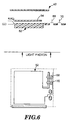
- Figure 6 illustrates the MOS structure of an individual pixel 42 which uses a N-well to P substrate photo-diode 52 to integrate photogenerated charge and employs a thin oxide capacitor 54 parallel with the photo-diode 52 to increase the charge handling capacity of the pixel.
- the signal charge is read-out to a common signal line using two series connected NMOS transistors 68, 70 which are controlled by row and column scanning registers integrated in the radiation detection panel 10.
- the pixel 42 has a size of 85 microns by 85 microns, of which the active area of the photo-diode 52 is about 63 microns by 63 microns (or 74% of the surface area).
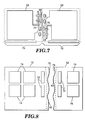
- Figure 7 illustrates two pixels of a tile 12.
- Pixel 72 is an edge pixel, i.e., a pixel located at the edge of the 624 by 624 pixel tile 12.
- Pixel 74 is an inside pixel, i.e., a pixel which is completely surrounded by other pixels 42, possibly including an edge pixel such as pixel 72.
- the gate oxide from transistors 68 and 70 is sensitive to the generation of additional carriers when positioned along the edge of the tile 12 and also due to narrow source/drain length.
- additional carriers are generated. This leads to a degradation in performance of the affected transistors 68 and 70.
- photo-diode 52 which has a much larger surface area, is much less sensitive to the generation of additional carriers. Therefore, edge pixels such as pixel 72 have transistors 68, 70 located opposite photo-diode 52 from the edge of tile 12. Such positioning reduces performance damage caused by the saw cut.
- Figure 8 illustrates edges 76 and 78 of adjacent tiles 12.
- the photo-sensitive area of inside pixels 74 are illustrated conventionally. For illustration purposes it appears that tiles 12 end just above the uppermost pixels 74. However, such is not the case. Tiles 12 extend substantially beyond the two partial rows of pixels shown. Therefore, all pixels labeled 74 are inside pixels.
- the photo-sensitive areas of edge pixels 72 are diminished in order to keep the center to center spacing of all pixels constant.
- the distance (center to center) between inside pixels 74, the distance (center to center) between an inside pixel 74 and an edge pixel 72, as well as the distance (center to center) between edge pixels 72 are constant. With constant spacing, pixel alignment will be constant regardless of a pixel is an inside pixel or an edge pixel.
- the size of the photo-sensitive area of edge pixels 72 are reduced in size. Image processing can make for the loss in detected sensitivity due to the reduction of the photo-sensitive area of edge pixels 72.
- a p/n diode junction 80 is established along the edge of each edge pixel 72 to passivate the additional carriers generated by the saw cut.
Landscapes
- Physics & Mathematics (AREA)
- Health & Medical Sciences (AREA)
- Life Sciences & Earth Sciences (AREA)
- General Physics & Mathematics (AREA)
- High Energy & Nuclear Physics (AREA)
- Molecular Biology (AREA)
- Spectroscopy & Molecular Physics (AREA)
- Measurement Of Radiation (AREA)
- Photometry And Measurement Of Optical Pulse Characteristics (AREA)
- Solid State Image Pick-Up Elements (AREA)
Claims (6)
- Festkörperstrahlungsdetektortafel zum Empfangen von Strahlung auf einer ersten Fläche, mit:dadurch gekennzeichnet, daßeinem gemeinsamen Substrat (14),mehreren Modulen (12), die mehrere Ränder aufweisen, wobei einige der mehreren Ränder einander unmittelbar benachbart angeordnet sind, wobei jedes der mehreren Module (12) eine Anordnung von Photodetektoren (42) aufweist, die in mehreren Reihen und Spalten angeordnet sind, wobei jeder Detektor ein Pixel repräsentiert und einen strahlungsempfindlichen Bereich zum Erzeugen eines Ausgangssignals (46) sowie eine nicht-strahlungsempfindliche Schaltungseinrichtung aufweist, die einem der Photodetektoren (42) zugeordnet ist,wobei diejenigen der Photodetektoren (42), die entlang einem Rand des Moduls (12) angeordnet sind, als Rand-Photodetektoren (42) bezeichnet werden, und diejenigen Photodetektoren (42, die innerhalb des Moduls (12) angeordnet sind, als Innen-Photodetektoren (42) bezeichnet werden,Schaltungseinrichtungen zum selektiven Adressieren eines der Photodetektoren (42) durch Adressieren einer der mehreren Reihen und einer der mehreren Spalten und durch Lesen des Ausgangssignals (46) des einen aus der Anordnung von Photodetektoren (42),einer Tafeladressiereinrichtung zum selektiven Adressieren eines der Photodetektoren (42) in jedem der mehreren Module (12) durch die Schaltungseinrichtung in jedem der mehreren Module (12),einer Tafelleseeinrichtung zum selektiven Lesen des Ausgangssignals (46) des einen aus der Anordnung von Photodetektoren (42) in jedem der Module, undeiner zwischen den mehreren Modulen (12) und dem gemeinsamen Substrat (14) angeordneten Verbindungseinrichtung zum Verbinden der Schaltungseinrichtung jedes der mehreren Module (12) mit der Tafeladressiereinrichtung beziehungsweise der Tafelleseeinrichtung,wobei jedes der mehreren Module (12) in einer dreidimensionalen Struktur angeordnet ist, in der die Anordnung von Photodetektoren (42) auf einer ersten Fläche jedes der mehreren Module (12) angeordnet ist, wobei sie im wesentlichen den gesamten Bereich der ersten Fläche bedecken, wobei die Schaltungseinrichtung innerhalb des Moduls (12) in einem Bereich angeordnet ist, der der empfangenen Strahlung abgewandt und von der ersten Fläche entfernt ist, und bei der die mehreren Module (12) einander unmittelbar benachbart angeordnet sind, woraus sich ein nahezu durchgehender strahlungsempfindlicher Bereich über die gesamte Fläche der die Strahlung empfangenden Festkörperstrahlungserkennungstafel (10) ergibt,die nicht strahlungsempfindliche Schaltungseinrichtung eines Rand-Photodetektors (42) an einem Rand desselben angeordnet ist, wobei der strahlungsempfindliche Bereich des Rand-Photodetektors (42) zwischen der nicht strahlungsempfindlichen Schaltungseinrichtung und dem Rand des Moduls (12) angeordnet ist.
- Festkörperstrahlungserkennungstafel nach Anspruch 1, durch eine Schicht aus Phosphor (16), die zwischen dem strahlungsempfindlichen Bereich der Module (12) und der empfangenen Strahlung angeordnet ist.
- Festkörperstrahlungserkennungstafel nach Anspruch 1 oder 2, dadurch gekennzeichnet, daß die strahlungsempfindlichen Bereiche der Rand-Photodetektoren (72) kleiner sind als die strahlungsempfindlichen Bereiche der Innen-Photodetektoren (74), und bei der Mittenabstand zwischen den strahlungsempfindlichen Bereichen benachbarter Photodetektoren (42) zwischen benachbarten Rand-Photodetektoren (72) sowie zwischen benachbarten Innen-Photodetektoren (74) im wesentlichen konstant gehalten ist.
- Festkörperstrahlungserkennungstafel nach einem der Ansprüche 1 bis 3, dadurch gekennzeichnet, daß jedes der Module (12) ferner eine p/n-Diode entlang dem Rand des Moduls (12) aufweist.
- Festkörperstrahlungserkennungstafel nach einem der Ansprüche 1 bis 4, dadurch gekennzeichnet, daß die Tafeladressiereinrichtung und die Tafelleseeinrichtung auf derjenigen Seite des gemeinsamen Substrats (14) angeordnet sind, die von den mehreren Modulen (12) abgewandt ist.
- Festkörperstrahlungserkennungstafel nach einem der Ansprüche 1 bis 5, dadurch gekennzeichnet, daß mehrere elektrische Kontaktelemente zwischen dem gemeinsamen Substrat (14) und den mehreren Modulen (12) angeordnet sind, wobei die mehreren elektrischen Kontaktelemente einen elektrischen Kontakt mit der Schaltungseinrichtung in jedem der mehreren Module (12) herstellen, und bei der ein flexibles Kabel (28) die mehreren elektrischen Kontaktelemente mit der Tafeladressiereinrichtung und der Tafelleseeinrichtung verbindet.
Applications Claiming Priority (2)
| Application Number | Priority Date | Filing Date | Title |
|---|---|---|---|
| US08/163,147 US5436458A (en) | 1993-12-06 | 1993-12-06 | Solid state radiation detection panel having tiled photosensitive detectors arranged to minimize edge effects between tiles |
| US163147 | 1993-12-06 |
Publications (2)
| Publication Number | Publication Date |
|---|---|
| EP0657938A1 EP0657938A1 (de) | 1995-06-14 |
| EP0657938B1 true EP0657938B1 (de) | 1998-06-10 |
Family
ID=22588691
Family Applications (1)
| Application Number | Title | Priority Date | Filing Date |
|---|---|---|---|
| EP94119021A Expired - Lifetime EP0657938B1 (de) | 1993-12-06 | 1994-12-02 | Festkörperstrahlungsdetektortafel mit matrixförmig angeordneten, lichtempfindlichen Detektoren, so angeordnet, dass Kanteneffekte zwischen den Elementen minimiert werden |
Country Status (5)
| Country | Link |
|---|---|
| US (2) | US5436458A (de) |
| EP (1) | EP0657938B1 (de) |
| JP (1) | JPH07209430A (de) |
| CA (1) | CA2135363A1 (de) |
| DE (1) | DE69410959T2 (de) |
Families Citing this family (67)
| Publication number | Priority date | Publication date | Assignee | Title |
|---|---|---|---|---|
| JP3066944B2 (ja) | 1993-12-27 | 2000-07-17 | キヤノン株式会社 | 光電変換装置、その駆動方法及びそれを有するシステム |
| JP2571018B2 (ja) * | 1994-05-31 | 1997-01-16 | 日本電気株式会社 | 固体撮像装置の製造方法 |
| GB2305096B (en) * | 1995-08-29 | 1997-09-10 | Simage Oy | Imaging system and method |
| US5635718A (en) * | 1996-01-16 | 1997-06-03 | Minnesota Mining And Manufacturing Company | Multi-module radiation detecting device and fabrication method |
| DE69623659T2 (de) | 1996-05-08 | 2003-05-08 | Ifire Technology Inc., Fort Saskatchewan | Hochauflösender flacher sensor für strahlungsabbildungssystem |
| US5650626A (en) * | 1996-07-16 | 1997-07-22 | Eastman Kodak Company | X-ray imaging detector with thickness and composition limited substrate |
| GB2318448B (en) | 1996-10-18 | 2002-01-16 | Simage Oy | Imaging detector and method of production |
| US5834782A (en) * | 1996-11-20 | 1998-11-10 | Schick Technologies, Inc. | Large area image detector |
| JP3805100B2 (ja) * | 1997-04-10 | 2006-08-02 | キヤノン株式会社 | 光電変換装置 |
| US5994713A (en) * | 1997-06-25 | 1999-11-30 | Quantum Imaging Corp. | Filmless photon imaging apparatus |
| US6198220B1 (en) | 1997-07-11 | 2001-03-06 | Emagin Corporation | Sealing structure for organic light emitting devices |
| US6252932B1 (en) * | 1997-07-22 | 2001-06-26 | Fuji Photo Film Co., Ltd. | Method and apparatus for acquiring image information for energy subtraction processing |
| US6144718A (en) * | 1997-11-26 | 2000-11-07 | General Electric Company | Flexible cable connection for detector module |
| GB2332608B (en) * | 1997-12-18 | 2000-09-06 | Simage Oy | Modular imaging apparatus |
| US6486470B2 (en) | 1998-11-02 | 2002-11-26 | 1294339 Ontario, Inc. | Compensation circuit for use in a high resolution amplified flat panel for radiation imaging |
| US6181773B1 (en) * | 1999-03-08 | 2001-01-30 | Direct Radiography Corp. | Single-stroke radiation anti-scatter device for x-ray exposure window |
| FR2793072B1 (fr) * | 1999-04-30 | 2001-11-30 | Commissariat Energie Atomique | Dispositif de detection compact pour gamma camera |
| FR2793071B1 (fr) | 1999-04-30 | 2001-06-08 | Commissariat Energie Atomique | Gamma camera miniature a detecteurs semiconducteurs |
| JP3838849B2 (ja) | 2000-03-28 | 2006-10-25 | 株式会社東芝 | X線平面検出器 |
| JP4447752B2 (ja) * | 2000-08-03 | 2010-04-07 | 浜松ホトニクス株式会社 | 放射線検出器 |
| US8909325B2 (en) | 2000-08-21 | 2014-12-09 | Biosensors International Group, Ltd. | Radioactive emission detector equipped with a position tracking system and utilization thereof with medical systems and in medical procedures |
| US8565860B2 (en) | 2000-08-21 | 2013-10-22 | Biosensors International Group, Ltd. | Radioactive emission detector equipped with a position tracking system |
| US8489176B1 (en) | 2000-08-21 | 2013-07-16 | Spectrum Dynamics Llc | Radioactive emission detector equipped with a position tracking system and utilization thereof with medical systems and in medical procedures |
| US6831263B2 (en) | 2002-06-04 | 2004-12-14 | Intel Corporation | Very high speed photodetector system using a PIN photodiode array for position sensing |
| JP2003017676A (ja) * | 2001-04-27 | 2003-01-17 | Canon Inc | 放射線撮像装置およびそれを用いた放射線撮像システム |
| US6657201B2 (en) * | 2001-06-29 | 2003-12-02 | General Electric Company | Cover plate having spacer lip with hermetic barrier for radiation imager and method of manufacturing same |
| JP4681774B2 (ja) * | 2001-08-30 | 2011-05-11 | キヤノン株式会社 | 撮像素子、その撮像素子を用いた撮像装置、及びその撮像装置を用いた撮像システム |
| DE10239506A1 (de) * | 2002-08-28 | 2004-03-18 | Infineon Technologies Ag | Sensoranordnung zum Erfassen einer Strahlung, Computertomograph mit dieser Sensoranordnung und zugehöriges Herstellungsverfahren |
| JP2005539232A (ja) * | 2002-09-18 | 2005-12-22 | コーニンクレッカ フィリップス エレクトロニクス エヌ ヴィ | 複数の検出器ユニットを有するx線検出器 |
| EP1550885B1 (de) * | 2002-09-26 | 2014-07-16 | Kabushiki Kaisha Toshiba | Leuchtstoffblatt für einen strahlungsdetektor; strahlungsdetektor damit und geräte zur detektion von strahlung |
| US7379528B2 (en) * | 2003-01-06 | 2008-05-27 | Koninklijke Philips Electronics N.V. | Radiation detector with shielded electronics for computed tomography |
| JP2004219318A (ja) * | 2003-01-16 | 2004-08-05 | Hamamatsu Photonics Kk | 放射線検出器 |
| KR101075626B1 (ko) * | 2003-05-23 | 2011-10-21 | 하마마츠 포토닉스 가부시키가이샤 | 광검출 장치 |
| CA2542581A1 (en) * | 2003-11-10 | 2005-05-26 | Ls Technologies, Inc. | Flat-panel detector utilizing electrically interconnecting tiled photosensor arrays |
| US20050098732A1 (en) * | 2003-11-10 | 2005-05-12 | Ls Technologies, Inc. | Flat-panel detector utilizing electrically interconnecting tiled photosensor arrays |
| US9040016B2 (en) | 2004-01-13 | 2015-05-26 | Biosensors International Group, Ltd. | Diagnostic kit and methods for radioimaging myocardial perfusion |
| US8571881B2 (en) | 2004-11-09 | 2013-10-29 | Spectrum Dynamics, Llc | Radiopharmaceutical dispensing, administration, and imaging |
| EP1709585B1 (de) | 2004-01-13 | 2020-01-08 | Spectrum Dynamics Medical Limited | Mehrdimensionale bildrekonstruktion |
| US8586932B2 (en) | 2004-11-09 | 2013-11-19 | Spectrum Dynamics Llc | System and method for radioactive emission measurement |
| US9470801B2 (en) | 2004-01-13 | 2016-10-18 | Spectrum Dynamics Llc | Gating with anatomically varying durations |
| US10964075B2 (en) | 2004-01-13 | 2021-03-30 | Spectrum Dynamics Llc | Gating with anatomically varying durations |
| US7196332B2 (en) * | 2004-05-04 | 2007-03-27 | General Electric Company | Monolithic x-ray detector with staggered detection areas |
| EP1778957A4 (de) | 2004-06-01 | 2015-12-23 | Biosensors Int Group Ltd | Optimierung der messung radioaktiver strahlung an besonderen körperstrukturen |
| EP1815270A2 (de) * | 2004-07-14 | 2007-08-08 | Orbotech Medical Solutions Ltd. | Strahlungsdetektor-kopf |
| US8606349B2 (en) | 2004-11-09 | 2013-12-10 | Biosensors International Group, Ltd. | Radioimaging using low dose isotope |
| US9943274B2 (en) | 2004-11-09 | 2018-04-17 | Spectrum Dynamics Medical Limited | Radioimaging using low dose isotope |
| US8615405B2 (en) | 2004-11-09 | 2013-12-24 | Biosensors International Group, Ltd. | Imaging system customization using data from radiopharmaceutical-associated data carrier |
| US9316743B2 (en) | 2004-11-09 | 2016-04-19 | Biosensors International Group, Ltd. | System and method for radioactive emission measurement |
| US10136865B2 (en) | 2004-11-09 | 2018-11-27 | Spectrum Dynamics Medical Limited | Radioimaging using low dose isotope |
| US8000773B2 (en) | 2004-11-09 | 2011-08-16 | Spectrum Dynamics Llc | Radioimaging |
| WO2008059489A2 (en) | 2006-11-13 | 2008-05-22 | Spectrum Dynamics Llc | Radioimaging applications of and novel formulations of teboroxime |
| US8837793B2 (en) | 2005-07-19 | 2014-09-16 | Biosensors International Group, Ltd. | Reconstruction stabilizer and active vision |
| EP1909853B1 (de) | 2005-07-19 | 2015-03-18 | Biosensors International Group, Ltd. | Bildgebungsprotokolle |
| US7745798B2 (en) * | 2005-11-15 | 2010-06-29 | Fujifilm Corporation | Dual-phosphor flat panel radiation detector |
| US8894974B2 (en) | 2006-05-11 | 2014-11-25 | Spectrum Dynamics Llc | Radiopharmaceuticals for diagnosis and therapy |
| US8492762B2 (en) * | 2006-06-27 | 2013-07-23 | General Electric Company | Electrical interface for a sensor array |
| WO2008075362A2 (en) | 2006-12-20 | 2008-06-26 | Spectrum Dynamics Llc | A method, a system, and an apparatus for using and processing multidimensional data |
| US8521253B2 (en) | 2007-10-29 | 2013-08-27 | Spectrum Dynamics Llc | Prostate imaging |
| JP5101402B2 (ja) | 2008-06-18 | 2012-12-19 | 浜松ホトニクス株式会社 | 固体撮像装置 |
| JP5376897B2 (ja) * | 2008-10-24 | 2013-12-25 | 富士フイルム株式会社 | 放射線画像撮影装置 |
| RU2510520C2 (ru) * | 2008-11-21 | 2014-03-27 | Трикселль | Способ сборки ячеистого радиационного детектора |
| US8117741B2 (en) * | 2009-04-07 | 2012-02-21 | Oy Ajat Ltd | Method for manufacturing a radiation imaging panel comprising imaging tiles |
| US8338788B2 (en) | 2009-07-29 | 2012-12-25 | Spectrum Dynamics Llc | Method and system of optimized volumetric imaging |
| WO2012145038A1 (en) * | 2011-04-19 | 2012-10-26 | Teledyne Rad-Icon Imaging Corp. | Method of direct silicon tiling of a tiled image sensor array |
| JP6305710B2 (ja) * | 2013-08-30 | 2018-04-04 | キヤノンメディカルシステムズ株式会社 | 検出器モジュール製造方法 |
| US10686003B2 (en) * | 2015-12-31 | 2020-06-16 | General Electric Company | Radiation detector assembly |
| DE102017124077B4 (de) * | 2017-10-17 | 2021-02-04 | Yxlon International Gmbh | Detektor mit verkleinerten Randpixel Elementen |
Family Cites Families (10)
| Publication number | Priority date | Publication date | Assignee | Title |
|---|---|---|---|---|
| US4467342A (en) * | 1982-07-15 | 1984-08-21 | Rca Corporation | Multi-chip imager |
| US4905265A (en) * | 1985-12-11 | 1990-02-27 | General Imaging Corporation | X-ray imaging system and solid state detector therefor |
| US5043582A (en) * | 1985-12-11 | 1991-08-27 | General Imagining Corporation | X-ray imaging system and solid state detector therefor |
| US5220170A (en) * | 1985-12-11 | 1993-06-15 | General Imaging Corporation | X-ray imaging system and solid state detector therefor |
| FR2598250B1 (fr) * | 1986-04-30 | 1988-07-08 | Thomson Csf | Panneau de prise de vue radiologique, et procede de fabrication |
| JP3013189B2 (ja) * | 1990-07-26 | 2000-02-28 | セイコーインスツルメンツ株式会社 | 密着型イメージセンサ |
| EP0473125B1 (de) * | 1990-08-30 | 1996-01-31 | Shimadzu Corporation | Strahlungsdetektor |
| US5329149A (en) * | 1990-10-12 | 1994-07-12 | Seiko Instruments Inc. | Image sensor with non-light-transmissive layer having photosensing windows |
| US5105087A (en) * | 1990-11-28 | 1992-04-14 | Eastman Kodak Company | Large solid state sensor assembly formed from smaller sensors |
| US5336879A (en) * | 1993-05-28 | 1994-08-09 | David Sarnoff Research Center, Inc. | Pixel array having image forming pixel elements integral with peripheral circuit elements |
-
1993
- 1993-12-06 US US08/163,147 patent/US5436458A/en not_active Expired - Fee Related
-
1994
- 1994-11-08 CA CA002135363A patent/CA2135363A1/en not_active Abandoned
- 1994-12-02 EP EP94119021A patent/EP0657938B1/de not_active Expired - Lifetime
- 1994-12-02 JP JP6299384A patent/JPH07209430A/ja active Pending
- 1994-12-02 DE DE69410959T patent/DE69410959T2/de not_active Expired - Fee Related
-
1995
- 1995-03-27 US US08/410,773 patent/US5545899A/en not_active Expired - Lifetime
Also Published As
| Publication number | Publication date |
|---|---|
| DE69410959D1 (de) | 1998-07-16 |
| JPH07209430A (ja) | 1995-08-11 |
| US5436458A (en) | 1995-07-25 |
| DE69410959T2 (de) | 1999-01-14 |
| CA2135363A1 (en) | 1995-06-07 |
| EP0657938A1 (de) | 1995-06-14 |
| US5545899A (en) | 1996-08-13 |
Similar Documents
| Publication | Publication Date | Title |
|---|---|---|
| US5436458A (en) | Solid state radiation detection panel having tiled photosensitive detectors arranged to minimize edge effects between tiles | |
| EP1073265B1 (de) | Bildaufnahmegerät | |
| US7842927B2 (en) | Image sensor, image-sensing apparatus using the image sensor, and image-sensing system | |
| EP0441521B1 (de) | Röntgen-Abbildungsvorrichtung aus Festkörperbauelementen | |
| US6671347B2 (en) | Radiation imaging apparatus and radiation imaging system using the same | |
| ES2704283T3 (es) | Dispositivo de formación de imágenes de rayos X y rayos gamma | |
| EP0986938B1 (de) | Röntgenstrahlungsdetektionssystem unter verwendung von aktiven bildsensoren | |
| US5942756A (en) | Radiation detector and fabrication method | |
| US6353228B1 (en) | Photosensor, and radiation detection apparatus and system | |
| KR101441630B1 (ko) | 엑스레이 검출기 및 이의 제조방법 | |
| EP0661556A2 (de) | Grosser Röntgenbildgeber und Methode seiner Herstellung | |
| EP0767389A2 (de) | Gerät zur Aufnahme von Röntgenbildern | |
| JP2003513472A (ja) | 完成度の高いコンタクトバイアを備え且つfetの光応答を低減したイメージャ | |
| EP1207560B1 (de) | Vorrichtung zur Umwandlung elektromagnetischer Wellen | |
| WO1994028583A1 (en) | Pixel array having image forming pixel elements integral with peripheral circuit elements | |
| US6600158B1 (en) | Semiconductor device and radiation image pickup system having the device | |
| US6354595B1 (en) | Method for tight sealing of a radiation detector and detector obtained by this method | |
| US6753915B1 (en) | Photoelectric Conversion Apparatus and Image Pickup Apparatus having an Optimally Positioned Driving Wire | |
| JPH09297181A (ja) | 放射線撮像装置 | |
| US6946661B2 (en) | Methods and apparatus for X-ray image detector assemblies | |
| JP2003218339A (ja) | 放射線検出装置 | |
| CN1973214B (zh) | 使用电互连的平铺光电传感器阵列的平板检测器 | |
| GB2317742A (en) | Imaging device | |
| JP2003309256A (ja) | 放射線検出装置及びその製造方法 | |
| JP2004228515A (ja) | 放射線検出装置 |
Legal Events
| Date | Code | Title | Description |
|---|---|---|---|
| PUAI | Public reference made under article 153(3) epc to a published international application that has entered the european phase |
Free format text: ORIGINAL CODE: 0009012 |
|
| AK | Designated contracting states |
Kind code of ref document: A1 Designated state(s): BE DE FR GB IT NL |
|
| 17P | Request for examination filed |
Effective date: 19951114 |
|
| 17Q | First examination report despatched |
Effective date: 19961009 |
|
| GRAG | Despatch of communication of intention to grant |
Free format text: ORIGINAL CODE: EPIDOS AGRA |
|
| GRAG | Despatch of communication of intention to grant |
Free format text: ORIGINAL CODE: EPIDOS AGRA |
|
| GRAH | Despatch of communication of intention to grant a patent |
Free format text: ORIGINAL CODE: EPIDOS IGRA |
|
| GRAH | Despatch of communication of intention to grant a patent |
Free format text: ORIGINAL CODE: EPIDOS IGRA |
|
| GRAA | (expected) grant |
Free format text: ORIGINAL CODE: 0009210 |
|
| RAP1 | Party data changed (applicant data changed or rights of an application transferred) |
Owner name: IMATION CORP. |
|
| AK | Designated contracting states |
Kind code of ref document: B1 Designated state(s): BE DE FR GB IT NL |
|
| PG25 | Lapsed in a contracting state [announced via postgrant information from national office to epo] |
Ref country code: NL Free format text: LAPSE BECAUSE OF FAILURE TO SUBMIT A TRANSLATION OF THE DESCRIPTION OR TO PAY THE FEE WITHIN THE PRESCRIBED TIME-LIMIT Effective date: 19980610 Ref country code: BE Free format text: LAPSE BECAUSE OF FAILURE TO SUBMIT A TRANSLATION OF THE DESCRIPTION OR TO PAY THE FEE WITHIN THE PRESCRIBED TIME-LIMIT Effective date: 19980610 |
|
| REF | Corresponds to: |
Ref document number: 69410959 Country of ref document: DE Date of ref document: 19980716 |
|
| ITF | It: translation for a ep patent filed | ||
| ET | Fr: translation filed | ||
| NLV1 | Nl: lapsed or annulled due to failure to fulfill the requirements of art. 29p and 29m of the patents act | ||
| PGFP | Annual fee paid to national office [announced via postgrant information from national office to epo] |
Ref country code: GB Payment date: 19981110 Year of fee payment: 5 |
|
| PGFP | Annual fee paid to national office [announced via postgrant information from national office to epo] |
Ref country code: FR Payment date: 19981203 Year of fee payment: 5 |
|
| PGFP | Annual fee paid to national office [announced via postgrant information from national office to epo] |
Ref country code: DE Payment date: 19981230 Year of fee payment: 5 |
|
| PLBE | No opposition filed within time limit |
Free format text: ORIGINAL CODE: 0009261 |
|
| STAA | Information on the status of an ep patent application or granted ep patent |
Free format text: STATUS: NO OPPOSITION FILED WITHIN TIME LIMIT |
|
| 26N | No opposition filed | ||
| PG25 | Lapsed in a contracting state [announced via postgrant information from national office to epo] |
Ref country code: GB Free format text: LAPSE BECAUSE OF NON-PAYMENT OF DUE FEES Effective date: 19991202 |
|
| GBPC | Gb: european patent ceased through non-payment of renewal fee |
Effective date: 19991202 |
|
| PG25 | Lapsed in a contracting state [announced via postgrant information from national office to epo] |
Ref country code: FR Free format text: LAPSE BECAUSE OF NON-PAYMENT OF DUE FEES Effective date: 20000831 |
|
| PG25 | Lapsed in a contracting state [announced via postgrant information from national office to epo] |
Ref country code: DE Free format text: LAPSE BECAUSE OF NON-PAYMENT OF DUE FEES Effective date: 20001003 |
|
| REG | Reference to a national code |
Ref country code: FR Ref legal event code: ST |
|
| PG25 | Lapsed in a contracting state [announced via postgrant information from national office to epo] |
Ref country code: IT Free format text: LAPSE BECAUSE OF NON-PAYMENT OF DUE FEES;WARNING: LAPSES OF ITALIAN PATENTS WITH EFFECTIVE DATE BEFORE 2007 MAY HAVE OCCURRED AT ANY TIME BEFORE 2007. THE CORRECT EFFECTIVE DATE MAY BE DIFFERENT FROM THE ONE RECORDED. Effective date: 20051202 |