EP0657996B1 - Etage amplificateur avec amplification ajustable - Google Patents
Etage amplificateur avec amplification ajustable Download PDFInfo
- Publication number
- EP0657996B1 EP0657996B1 EP94119072A EP94119072A EP0657996B1 EP 0657996 B1 EP0657996 B1 EP 0657996B1 EP 94119072 A EP94119072 A EP 94119072A EP 94119072 A EP94119072 A EP 94119072A EP 0657996 B1 EP0657996 B1 EP 0657996B1
- Authority
- EP
- European Patent Office
- Prior art keywords
- transistors
- reference voltage
- terminal
- series
- transistor
- Prior art date
- Legal status (The legal status is an assumption and is not a legal conclusion. Google has not performed a legal analysis and makes no representation as to the accuracy of the status listed.)
- Expired - Lifetime
Links
- 230000003321 amplification Effects 0.000 title description 3
- 238000003199 nucleic acid amplification method Methods 0.000 title description 3
- 230000002787 reinforcement Effects 0.000 description 3
- 239000003990 capacitor Substances 0.000 description 2
- 238000011161 development Methods 0.000 description 2
- 230000018109 developmental process Effects 0.000 description 2
- 230000002238 attenuated effect Effects 0.000 description 1
- 238000005516 engineering process Methods 0.000 description 1
- 238000010295 mobile communication Methods 0.000 description 1
- 239000004065 semiconductor Substances 0.000 description 1
Images


Classifications
-
- H—ELECTRICITY
- H03—ELECTRONIC CIRCUITRY
- H03G—CONTROL OF AMPLIFICATION
- H03G1/00—Details of arrangements for controlling amplification
- H03G1/04—Modifications of control circuit to reduce distortion caused by control
-
- H—ELECTRICITY
- H03—ELECTRONIC CIRCUITRY
- H03G—CONTROL OF AMPLIFICATION
- H03G1/00—Details of arrangements for controlling amplification
- H03G1/0005—Circuits characterised by the type of controlling devices operated by a controlling current or voltage signal
- H03G1/0017—Circuits characterised by the type of controlling devices operated by a controlling current or voltage signal the device being at least one of the amplifying solid-state elements
- H03G1/0023—Circuits characterised by the type of controlling devices operated by a controlling current or voltage signal the device being at least one of the amplifying solid-state elements in emitter-coupled or cascode amplifiers
-
- H—ELECTRICITY
- H03—ELECTRONIC CIRCUITRY
- H03G—CONTROL OF AMPLIFICATION
- H03G1/00—Details of arrangements for controlling amplification
- H03G1/0005—Circuits characterised by the type of controlling devices operated by a controlling current or voltage signal
- H03G1/0088—Circuits characterised by the type of controlling devices operated by a controlling current or voltage signal using discontinuously variable devices, e.g. switch-operated
Definitions
- the invention relates to a low-noise, in the gain switchable amplifier stage according to the preamble of Claim 1.
- Such a differential amplifier is known from DE 32 04 430 A1 known of a cascode stage and a reference voltage source having.
- Such low noise amplifier stages are particularly in high-frequency technology for receiving circuits, e.g. in mobile communications for frequency ranges e.g. up to 2 GHz.
- JP-A-1 288 101 An integrable amplifier stage which can be switched over in gain is known from JP-A-1 288 101.
- the object of the present invention is a special version of a in reinforcement switchable integrable amplifier stage specify.
- the advantage of the invention is that when changing the gain the input impedance of the circuit is hardly changed.
- 1 is, for example, a supply voltage terminal referred to, which supplies a reference voltage source 2.
- the reference voltage of the reference voltage source 2 is at one Terminal 3 can be tapped and becomes two further reference voltage sources 4 and 5 fed. These each generate on their Outputs 6 and 7 two independent reference voltages.
- the first reference voltage at the output terminal 6 is fed to the base terminals of NPN transistors 12 to 21.
- the collectors of the transistors 12 to 21 are together and via a parallel resonant circuit 43, 44, which is connected externally to the Circuit can be coupled with a further supply voltage terminal 42 connected.
- This supply voltage terminal 42 can also match supply voltage terminal 1.
- an output terminal 46 is provided via a capacity 45 with the interconnected collectors of transistors 12 to 21 is connected.
- the on the Output terminal 7 tapped second reference voltage is over a choke coil 9 the base connections of NPN transistors 22 to 31 fed.
- the collector of transistor 22 is with connected to the emitter of transistor 12.
- the collectors of the Transistors 23 to 31 and the emitters of transistors 13 to 21 are connected.
- Each emitter of the transistors 22 to 31 is through a resistor 32 to 41 with ground interconnected.
- An input terminal 11 is provided, which via a capacitance 10 with the base terminals of the transistors 22 to 31 is connected.
- the output terminal 7 of the second reference voltage source is also with a capacity 8 with Ground connected.
- the voltage supply terminal 42 is over Capacitance 47 connected to a control input terminal 50. Furthermore, it is with the collectors of transistors 48 and 49 connected.
- the base connections of transistors 48 and 49 are connected to the control input terminal 50.
- the emitters of transistors 48 and 49 are with the emitters of the transistors 13 to 21 interconnected.
- the control input terminal 50 is over a series circuit consisting of a resistor 51 and a diode 52 connected in the direction of flow connected to ground.
- the reference voltage at output terminal 3 can e.g. by a bandgap circuit independent of temperature and supply voltage his. This reference voltage is then used for generation of the two further reference voltages at the output terminals 6 and 7.
- the reference voltage reaches the output terminal 7 via the choke 9 to the base of the transistors 22-31
- Reference voltage at the output terminal 6 is directly the first Input one through transistors 12 through 21 and 48, 49 Formed differential amplifier stage supplied, the Capacitor 72 (Fig. 3) for high frequency grounding of the bases serves in transistor 12-21.
- the Amplification of the differential amplifier stage can be switched.
- the frequency signal to be amplified is input terminal 11 fed in and attenuated or amplified via the cascode level. In the example shown, this can e.g.
- the resonant circuit 43, 44 is connected to the supply voltage and determines with its quality and the decoupling used the maximum gain of the low noise amplifier.
- the capacitance 47 serves to block unwanted disturbances, resistors 32 to 41 to increase current feedback, i.e. for linearization, the lower cascode transistors 22 to 31.
- the combination of resistor 51 and that as a diode switched transistor 52 pulls the potential at the control input terminal 50 with control switched off approx. 0.5 Volts, which corresponds to a logic "0" level, and so switches the maximum gain of the low noise amplifier.
- the gain setting is made by separating the Collector lines of transistors 22 and transistors 23 to 31 achieved via the cascode transistors 12 and 13 to 21. If the transistors 48 and 49 are in the off state, the flows whole direct and signal alternating current via the collector lines of the transistors 22 to 31 and via that of the transistors 12 to 21 to the exit, i.e. to the short-circuited collectors of transistors 12 to 21. This corresponds to the state of maximum Reinforcement. Is via the switching input 50, by a High level, switched to minimal gain, then flows the collector direct and alternating current of the transistors 23 to 31 via the cascode transistors 48 and 49, while the transistors 13 to 21 are blocked, so that only the DC and AC component of the transistor 22 via the Transistor 12 can drain. The distribution of the collector lines the transistors 22 to 31 was in the example shown set to a gain change value of 20 dB.
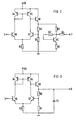
- FIG. 2 shows an embodiment of a reference voltage source according to reference number 5 in FIG. 1.
- This reference voltage source has a supply voltage terminal 53 which with the supply voltage terminal 42 or 1 according to FIG. 1 can be identical. This is with the emitters of two pnp transistors 54 and 55 interconnected. The basic connections of the two transistors 54 and 55 are with each other and with the Collector of transistor 54 connected. The collector of the transistor 54 is still with the collector of an NPN transistor 56 interconnected. The base of transistor 56 is with an input terminal 3 interconnected. The collector of the transistor 55 is with the collector of an NPN transistor 57 connected. The emitter of transistor 57 is with the emitter of transistor 56 and connected via a resistor 60 Ground connected.
- the supply voltage terminal 53 is also connected to the collector of an NPN transistor 58.
- the emitter is connected through a resistor 59 to the base of the Transistor 57 connected.
- the base of transistor 58 is connected to the collector of transistor 55.
- the basis of the Transistor 57 is connected to ground via a resistor 61.
- the output signal of the reference voltage source is on
- the emitter of transistor 58 is tapped and connected in series two resistors 62 and 64 of an output terminal 7 fed.
- the collector of an NPN transistor 65 is connected.
- the base of transistor 65 is through a resistor 63 connected to its collector.
- the emitter of transistor 65 is connected to ground via a resistor 66.
- the reference voltage source shown in FIG. 2 is used to to set the operating points of the transistors 22 to 31. This is via a thermally coupled current mirror circuit the transistor 65 realized. The base of the transistors 22 to 31 are then through the resistor 64 and the external Throttle element 9 supplied. Resistor 66 preferably has the same value as resistors 32 to 41 and the Resistor 63 is preferably ten times the resistance 64.
- FIG. 3 shows an embodiment for a reference voltage source according to the symbol 4 from Figure 1.
- the arrangement corresponds essentially that of Figure 2, so that like elements are the same Have reference numerals.
- the output voltage at the emitter of the transistor 58 fed directly to the output terminal 6.
- an integrable capacitance 72 switched, which is used to block unwanted interference.
- FIG. 4 is only partially the switchable differential amplifier according to Figure 1 shown.
- the same elements have the same reference numerals on.
- the second differential amplifier stage is here for example only from two transistors connected in series 13 and 23.
- further switchable stages are provided. However, only one is shown consisting of the series connection connected in parallel to the other two stages from the load paths of transistors 67 and 68 and the Resistor 69.
- the node of the load paths of the transistors 13 and 23 is controlled symbolically via terminal 70.
- An arrangement according to FIG. 1 can exist here, for example be provided from elements 47 to 52. In the same way and way the node of the load paths of the transistors 67 and 68 by a similar arrangement via terminal 71 can be controlled.
Landscapes
- Amplifiers (AREA)
- Control Of Amplification And Gain Control (AREA)
Claims (3)
- Etage amplificateur à faible bruit avec amplification ajustable monté en cascode,avec un premier montage en série des circuits de charge de deux transistors (12, 22) et d'une première résistance (32), laquelle est reliée à une borne de potentiel de référence,avec au moins un deuxième montage en série des circuits de charge de deux transistors (13 ... 21, 23 ... 31 ; 67, 68) et d'une deuxième résistance (33 ... 41 ; 69), laquelle est reliée à la borne de potentiel de référence, le deuxième montage en série étant monté en parallèle avec le premier montage en série (12, 22, 32),dans lequel les bornes de collecteur de chacun des premiers transistors (12 ... 21 ; 67) des montages en série sont montées en parallèle et couplées à une borne de sortie (46), la borne de sortie (46) étant reliée via un circuit oscillant (43, 44) à une borne de tension d'alimentation (42),avec une première et une deuxième source de tension de référence (4, 5), la première source de tension de référence étant amenée aux bornes de base de chacun des premiers transistors (12 ... 21 ; 67) des montages en série et la deuxième tension de référence étant amenée aux bornes de base de chacun des deuxièmes transistors (22 ... 31 ; 68) des montages en série, les bornes de base de chacun des deuxièmes transistors des montages en série étant couplées à une borne d'entrée (11),dans lequel au moins un moyen de commutation (48, 49, 51, 52) relie en fonction d'un signal de commande, le point de liaison des circuits de charge des transistors de chaque deuxième montage en série à la borne de tension d'alimentation (42).
- Etage amplificateur selon la revendication 1, dans lequel le deuxième montage en série est composé d'une pluralité de premiers et de deuxièmes transistors montés en parallèle.
- Etage amplificateur selon l'une des revendications précédentes, dans lequel la deuxième tension de référence est amenée via une inductance aux bornes de base de chacun des deuxièmes transistors des montages en série.
Applications Claiming Priority (2)
| Application Number | Priority Date | Filing Date | Title |
|---|---|---|---|
| DE4341507A DE4341507C1 (de) | 1993-12-06 | 1993-12-06 | Verstärkerstufe |
| DE4341507 | 1993-12-06 |
Publications (3)
| Publication Number | Publication Date |
|---|---|
| EP0657996A2 EP0657996A2 (fr) | 1995-06-14 |
| EP0657996A3 EP0657996A3 (fr) | 1996-02-07 |
| EP0657996B1 true EP0657996B1 (fr) | 2001-04-11 |
Family
ID=6504277
Family Applications (1)
| Application Number | Title | Priority Date | Filing Date |
|---|---|---|---|
| EP94119072A Expired - Lifetime EP0657996B1 (fr) | 1993-12-06 | 1994-12-02 | Etage amplificateur avec amplification ajustable |
Country Status (3)
| Country | Link |
|---|---|
| US (1) | US5459433A (fr) |
| EP (1) | EP0657996B1 (fr) |
| DE (2) | DE4341507C1 (fr) |
Families Citing this family (9)
| Publication number | Priority date | Publication date | Assignee | Title |
|---|---|---|---|---|
| US5920230A (en) * | 1997-10-21 | 1999-07-06 | Trw Inc. | HEMT-HBT cascode distributed amplifier |
| US6144254A (en) * | 1999-06-04 | 2000-11-07 | Infineon Technologies Corporation | Low-noise amplifier with switched gain and method |
| US6271726B1 (en) * | 2000-01-10 | 2001-08-07 | Conexant Systems, Inc. | Wideband, variable gain amplifier |
| US6404283B1 (en) | 2000-08-18 | 2002-06-11 | Motorola, Inc. | Method and apparatus for amplifying a radio frequency signal |
| US6424222B1 (en) * | 2001-03-29 | 2002-07-23 | Gct Semiconductor, Inc. | Variable gain low noise amplifier for a wireless terminal |
| FI20011866A0 (fi) * | 2001-09-21 | 2001-09-21 | Nokia Corp | Monituloinen vahvistin |
| US20090251218A1 (en) * | 2008-04-03 | 2009-10-08 | Paulo Oliveira | Variable Gain Amplifier |
| US7889008B2 (en) * | 2009-06-08 | 2011-02-15 | Mediatek Inc. | Programmable gain MOS amplifier |
| US8854144B2 (en) | 2012-09-14 | 2014-10-07 | General Atomics | High voltage amplifiers and methods |
Family Cites Families (3)
| Publication number | Priority date | Publication date | Assignee | Title |
|---|---|---|---|---|
| DE3204430A1 (de) * | 1982-02-09 | 1983-08-18 | Siemens AG, 1000 Berlin und 8000 München | Integrierbarer differenzverstaerker |
| US4520324A (en) * | 1983-03-11 | 1985-05-28 | National Semiconductor Corporation | MOS Gain controlled amplifier |
| JPH01288101A (ja) * | 1988-05-16 | 1989-11-20 | Iwatsu Electric Co Ltd | ゲイン切替回路 |
-
1993
- 1993-12-06 DE DE4341507A patent/DE4341507C1/de not_active Expired - Fee Related
-
1994
- 1994-12-02 DE DE59409726T patent/DE59409726D1/de not_active Expired - Lifetime
- 1994-12-02 EP EP94119072A patent/EP0657996B1/fr not_active Expired - Lifetime
- 1994-12-06 US US08/349,898 patent/US5459433A/en not_active Expired - Lifetime
Also Published As
| Publication number | Publication date |
|---|---|
| US5459433A (en) | 1995-10-17 |
| DE59409726D1 (de) | 2001-05-17 |
| EP0657996A3 (fr) | 1996-02-07 |
| EP0657996A2 (fr) | 1995-06-14 |
| DE4341507C1 (de) | 1995-02-23 |
Similar Documents
| Publication | Publication Date | Title |
|---|---|---|
| DE60027128T2 (de) | Verstärker mit veränderbarer verstärkung und erhöhter linearität | |
| DE69706954T2 (de) | Niederspannungs-Gegentaktmischer | |
| EP0579686B1 (fr) | Circuit de transducteur | |
| DE69431905T2 (de) | Leitungstreiber mit adaptiver ausgangsimpedanz | |
| DE69224677T2 (de) | Programmierbarer Verstärker | |
| DE2549575C2 (de) | Transistorschaltung | |
| EP0288016A2 (fr) | Comparateur avec domaine étendu de signal d'entrée à mode commun | |
| DE60021170T2 (de) | Verstärker | |
| DE69023061T2 (de) | Pufferverstärker mit niedrigem Ausgangswiderstand. | |
| DE3502915A1 (de) | Verstaerker zur korrektur der gruppenlaufzeit elektrischer signale | |
| DE1901804A1 (de) | Stabilisierter Differentialverstaerker | |
| DE69113523T2 (de) | Emittergeerdete Verstärkerschaltung mit Vorspannungsschaltung. | |
| DE3116230C2 (de) | Regelbare Verstärkerschaltung | |
| DE4341507C1 (de) | Verstärkerstufe | |
| DE68920399T2 (de) | Filterschaltungsanordnung. | |
| WO2001022573A1 (fr) | Montage permettant de regler le point de fonctionnement d'un amplificateur de puissance | |
| DE69821197T2 (de) | Differenzverstärker, integrierte schaltung und telefon | |
| EP0252540B1 (fr) | Dispositif de circuit pour l'ajustage d'un niveau de référence dans un signal périodique | |
| DE69119169T2 (de) | Verstärkerschaltung | |
| DE69315553T2 (de) | Differenzverstärkeranordnung | |
| DE2924171C2 (fr) | ||
| DE3234400A1 (de) | Halbleiter-verstaerkerschaltung | |
| DE2946952C2 (fr) | ||
| DE3210453C2 (de) | Signal-Eingangsschaltung | |
| DE69721898T2 (de) | Verstärker mit variabler Verstärkung und geringer Gleichspannungsabweichung am Ausgang und geringen Verzerrungen |
Legal Events
| Date | Code | Title | Description |
|---|---|---|---|
| PUAI | Public reference made under article 153(3) epc to a published international application that has entered the european phase |
Free format text: ORIGINAL CODE: 0009012 |
|
| AK | Designated contracting states |
Kind code of ref document: A2 Designated state(s): DE FR GB IT |
|
| PUAL | Search report despatched |
Free format text: ORIGINAL CODE: 0009013 |
|
| AK | Designated contracting states |
Kind code of ref document: A3 Designated state(s): DE FR GB IT |
|
| 17P | Request for examination filed |
Effective date: 19960807 |
|
| 17Q | First examination report despatched |
Effective date: 19990312 |
|
| RTI1 | Title (correction) |
Free format text: AMPLIFYING STAGE WITH ADJUSTABLE AMPLIFICATION |
|
| GRAG | Despatch of communication of intention to grant |
Free format text: ORIGINAL CODE: EPIDOS AGRA |
|
| GRAG | Despatch of communication of intention to grant |
Free format text: ORIGINAL CODE: EPIDOS AGRA |
|
| GRAH | Despatch of communication of intention to grant a patent |
Free format text: ORIGINAL CODE: EPIDOS IGRA |
|
| RAP1 | Party data changed (applicant data changed or rights of an application transferred) |
Owner name: INFINEON TECHNOLOGIES AG |
|
| GRAH | Despatch of communication of intention to grant a patent |
Free format text: ORIGINAL CODE: EPIDOS IGRA |
|
| GRAA | (expected) grant |
Free format text: ORIGINAL CODE: 0009210 |
|
| RAP1 | Party data changed (applicant data changed or rights of an application transferred) |
Owner name: INFINEON TECHNOLOGIES AG |
|
| AK | Designated contracting states |
Kind code of ref document: B1 Designated state(s): DE FR GB IT |
|
| REF | Corresponds to: |
Ref document number: 59409726 Country of ref document: DE Date of ref document: 20010517 |
|
| ET | Fr: translation filed | ||
| ITF | It: translation for a ep patent filed | ||
| GBT | Gb: translation of ep patent filed (gb section 77(6)(a)/1977) |
Effective date: 20010627 |
|
| REG | Reference to a national code |
Ref country code: GB Ref legal event code: IF02 |
|
| PLBE | No opposition filed within time limit |
Free format text: ORIGINAL CODE: 0009261 |
|
| STAA | Information on the status of an ep patent application or granted ep patent |
Free format text: STATUS: NO OPPOSITION FILED WITHIN TIME LIMIT |
|
| 26N | No opposition filed | ||
| PG25 | Lapsed in a contracting state [announced via postgrant information from national office to epo] |
Ref country code: IT Free format text: LAPSE BECAUSE OF NON-PAYMENT OF DUE FEES;WARNING: LAPSES OF ITALIAN PATENTS WITH EFFECTIVE DATE BEFORE 2007 MAY HAVE OCCURRED AT ANY TIME BEFORE 2007. THE CORRECT EFFECTIVE DATE MAY BE DIFFERENT FROM THE ONE RECORDED. Effective date: 20051202 |
|
| REG | Reference to a national code |
Ref country code: FR Ref legal event code: TP Owner name: INTEL MOBILE COMMUNICATIONS GMBH, DE Effective date: 20120404 Ref country code: FR Ref legal event code: CA Effective date: 20120404 |
|
| REG | Reference to a national code |
Ref country code: GB Ref legal event code: 732E Free format text: REGISTERED BETWEEN 20120607 AND 20120613 |
|
| REG | Reference to a national code |
Ref country code: GB Ref legal event code: 732E Free format text: REGISTERED BETWEEN 20121213 AND 20121219 |
|
| REG | Reference to a national code |
Ref country code: DE Ref legal event code: R081 Ref document number: 59409726 Country of ref document: DE Owner name: INTEL MOBILE COMMUNICATIONS GMBH, DE Free format text: FORMER OWNER: INFINEON TECHNOLOGIES AG, 81669 MUENCHEN, DE Effective date: 20130314 Ref country code: DE Ref legal event code: R081 Ref document number: 59409726 Country of ref document: DE Owner name: INTEL MOBILE COMMUNICATIONS GMBH, DE Free format text: FORMER OWNER: INTEL MOBILE COMMUNICATIONS TECHNOLOGY GMBH, 85579 NEUBIBERG, DE Effective date: 20130326 Ref country code: DE Ref legal event code: R081 Ref document number: 59409726 Country of ref document: DE Owner name: INTEL MOBILE COMMUNICATIONS GMBH, DE Free format text: FORMER OWNER: INTEL MOBILE COMMUNICATIONS GMBH, 85579 NEUBIBERG, DE Effective date: 20130315 Ref country code: DE Ref legal event code: R081 Ref document number: 59409726 Country of ref document: DE Owner name: INTEL MOBILE COMMUNICATIONS GMBH, DE Free format text: FORMER OWNER: INFINEON TECHNOLOGIES AG, 85579 NEUBIBERG, DE Effective date: 20130315 |
|
| PGFP | Annual fee paid to national office [announced via postgrant information from national office to epo] |
Ref country code: DE Payment date: 20131127 Year of fee payment: 20 Ref country code: GB Payment date: 20131127 Year of fee payment: 20 |
|
| PGFP | Annual fee paid to national office [announced via postgrant information from national office to epo] |
Ref country code: FR Payment date: 20131209 Year of fee payment: 20 |
|
| REG | Reference to a national code |
Ref country code: DE Ref legal event code: R071 Ref document number: 59409726 Country of ref document: DE |
|
| REG | Reference to a national code |
Ref country code: GB Ref legal event code: PE20 Expiry date: 20141201 |
|
| PG25 | Lapsed in a contracting state [announced via postgrant information from national office to epo] |
Ref country code: GB Free format text: LAPSE BECAUSE OF EXPIRATION OF PROTECTION Effective date: 20141201 |
|
| REG | Reference to a national code |
Ref country code: FR Ref legal event code: CD Owner name: INTEL DEUTSCHLAND GMBH, DE Effective date: 20160126 |