EP0658046A2 - Vorrichtung und Verfahen zum Verarbeiten eines Videosignals und Vorrichtung zum Aufzeichnen und Wiedergeben von Videosignalen damit - Google Patents
Vorrichtung und Verfahen zum Verarbeiten eines Videosignals und Vorrichtung zum Aufzeichnen und Wiedergeben von Videosignalen damit Download PDFInfo
- Publication number
- EP0658046A2 EP0658046A2 EP94118560A EP94118560A EP0658046A2 EP 0658046 A2 EP0658046 A2 EP 0658046A2 EP 94118560 A EP94118560 A EP 94118560A EP 94118560 A EP94118560 A EP 94118560A EP 0658046 A2 EP0658046 A2 EP 0658046A2
- Authority
- EP
- European Patent Office
- Prior art keywords
- video signal
- synchronizing signal
- signal
- synchronizing
- separating
- Prior art date
- Legal status (The legal status is an assumption and is not a legal conclusion. Google has not performed a legal analysis and makes no representation as to the accuracy of the status listed.)
- Granted
Links
Images







Classifications
-
- H—ELECTRICITY
- H04—ELECTRIC COMMUNICATION TECHNIQUE
- H04N—PICTORIAL COMMUNICATION, e.g. TELEVISION
- H04N5/00—Details of television systems
- H04N5/76—Television signal recording
- H04N5/91—Television signal processing therefor
- H04N5/93—Regeneration of the television signal or of selected parts thereof
- H04N5/937—Regeneration of the television signal or of selected parts thereof by assembling picture element blocks in an intermediate store
-
- H—ELECTRICITY
- H04—ELECTRIC COMMUNICATION TECHNIQUE
- H04N—PICTORIAL COMMUNICATION, e.g. TELEVISION
- H04N5/00—Details of television systems
- H04N5/04—Synchronising
- H04N5/08—Separation of synchronising signals from picture signals
-
- H—ELECTRICITY
- H04—ELECTRIC COMMUNICATION TECHNIQUE
- H04N—PICTORIAL COMMUNICATION, e.g. TELEVISION
- H04N5/00—Details of television systems
- H04N5/14—Picture signal circuitry for video frequency region
- H04N5/21—Circuitry for suppressing or minimising disturbance, e.g. moiré or halo
-
- H—ELECTRICITY
- H04—ELECTRIC COMMUNICATION TECHNIQUE
- H04N—PICTORIAL COMMUNICATION, e.g. TELEVISION
- H04N5/00—Details of television systems
- H04N5/44—Receiver circuitry for the reception of television signals according to analogue transmission standards
- H04N5/46—Receiver circuitry for the reception of television signals according to analogue transmission standards for receiving on more than one standard at will
Definitions
- the present invention relates to a video signal processing apparatus and a video signal processing method wherein processing in the direction of time axis is performed by delaying only the effective picture period of standard video signal, and also relates to a video signal recording/reproduction apparatus incorporating such a video signal processing apparatus.
- Apparatus for improving video signal quality include a video signal processing apparatus of the type that performs arithmetic operations in the direction of time axis, for example, a three-dimensional luminance and chrominance signal separation filter, video signal noise suppressor, and field or frame interpolation apparatus.
- FIG. 1 is a block diagram showing a prior art configuration of such a video signal processing apparatus
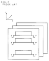
- FIG. 2 is a schematic diagram showing a video signal in three-dimensional space.
- the direction of time axis in the video signal is the direction of t axis, which is sometimes called the field direction or the frame direction.
- the video signal processing apparatus of the prior art shown in FIG. 1 is an example of such a configuration wherein only the effective picture period is stored in the memory circuit and arithmetic operations are performed in the direction of time axis.
- the numeral 1 indicates an input terminal via which a video signal is inputted, and 2 designates an output terminal via which the video signal after arithmetic operations is outputted.
- the video signal input via the inputted terminal 1, is fed to a synchronizing signal separation circuit 8, a memory circuit 10, and an arithmetic circuit 11, respectively.
- the synchronizing signal separation circuit 8 separates a synchronizing signal from the input video signal, and supplies the separated synchronizing signal to a reset circuit 6.
- the reset circuit 6 outputs a reset pulse to a counter circuit 7 in synchronism with the synchronizing signal.
- the counter circuit 7 performs a counting action upon reception of the reset pulse, and supplies the count value to a memory control circuit 9.
- the memory control circuit 9 controls the memory circuit 10 in accordance with the count value.
- the memory circuit 10 is a storage circuit having the capacity necessary for delaying the input video signal in the direction of time axis, and under the control of the memory control circuit 9, supplies the video signal delayed in the direction of time axis to the arithmetic circuit 11.
- the arithmetic circuit 11 performs arithmetic operations in the direction of time axis on the video signal supplied via the input terminal 1 and the delayed video signal outputted from the memory circuit 10, and outputs the thus processed video signal at the output terminal 2.
- the standard video signal is applied at the input terminal 1.
- the standard video signal is a video signal for which the relations defined by the following equations (1) and (2) hold among the color subcarrier frequency fsc, horizontal synchronizing signal frequency fh, and vertical synchronizing frequency fv.
- fsc (455/2)fh Equation (1)
- fh (525/2)fv Equation (2)
- a pulse signal synchronized to the color subcarrier of the input video signal and having a frequency equal to a multiple thereof is used as the clock.
- FIG. 3 is a timing chart illustrating the operation of the various circuit blocks.
- the video signal inputted via the input terminal 1, is fed to the synchronizing signal separation circuit 8, the memory circuit 10, and the arithmetic circuit 11, respectively.
- the synchronizing signal separation circuit 8 separates a vertical synchronizing signal from the input video signal, and supplies the separated vertical synchronizing signal to the reset circuit 6.
- the reset circuit 6 outputs a reset pulse to reset the counter circuit 7.
- the memory control circuit 9 outputs a control signal for a predetermined portion of the video signal to be written into the memory circuit 10, and a control signal for delaying the video signal in the direction of time axis when read out of the memory circuit 10; these control signals are supplied to the memory circuit 10. Then, in the arithmetic circuit 11, arithmetic operations in the direction of time axis are performed between the input video signal from the input terminal 1 and the video signal from the memory circuit 10 delayed in the direction of time axis, and the resulting video signal is outputted at the output terminal 2.
- FIG. 4 is a diagram showing the positional relationship in the direction of time axis between the input video signal and the video signal outputted from the memory circuit 10.
- arithmetic operations in the direction of time axis are arithmetic operations performed between a and a' between b and b', and between c and c', respectively.
- the time spacing between arithmetic data is equal to an integral multiple of the field period 1/fv.
- the arithmetic operations performed here include, for example, three-dimensional luminance and chrominance signal separation, noise elimination, etc.
- the portion of the video signal to be written into the memory circuit 10 is determined on the basis of the synchronizing signal that the synchronizing signal separation circuit separates from the video signal.
- the timing called jitter
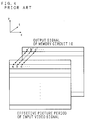
- FIG. 5 shows the positional relationship in the direction of time axis between the input video signal and the video signal outputted from the memory circuit 10 when jitter is caused on the synchronizing signal.
- the output video signal should be stored in the memory circuit 10 as a', b', c' ..., but when jitter is caused on the synchronizing signal, the signal is stored as b', c', d' ..., in which case arithmetic operations are performed between a and b', between b and c', and between c and d'.
- the resulting problem is that the time spacing between the input video signal and the video signal outputted from the memory circuit 10 is no longer equal to an integral multiple of the field period, and therefore, arithmetic operations between the input video signal and the video signal outputted from the memory circuit 10 are not performed in the correct time axis direction in the arithmetic circuit 11.
- a video signal processing apparatus has synchronizing signal separating means for separating a first synchronizing signal from an input video signal, and synchronizing signal generating means for generating a second synchronizing signal having substantially the same cycle as the first synchronizing signal when a prescribed time has elapsed after the separation of the first synchronizing signal.
- the input video signal is stored by switching selection between the first synchronizing signal separated from the input video signal and the second synchronizing signal generated when the prescribed time has elapsed after the separation of the first synchronizing signal and having substantially the same cycle as the first synchronizing signal. Accordingly, the input video signal can be stored correctly without being affected by variations in the synchronizing signal cycle that cause variations in signal write position.
- a video signal processing apparatus which is a modification of the video signal processing apparatus of the first invention
- the input video signal is stored on the basis of the first synchronizing signal
- the input video signal is stored on the basis of the second synchronizing signal. Accordingly, the input video signal is stored on the basis of stable synchronizing signal free from timing variations.
- a video signal processing apparatus has: arithmetic means for performing arithmetic operations between input video signals displaced from each other in the direction of time axis; synchronizing signal separating means for separating a synchronizing signal from the current input signal; synchronizing signal generating means for generating a synchronizing signal independently of the input video signal; and means for obtaining a delayed input video signal by switching selection between the synchronizing signal from the synchronizing signal separating means and the synchronizing signal from the synchronizing signal generating means.
- the delayed input video signal is obtained by switching selection between the two synchronizing signals, the time difference between the current input video signal and the delayed video signal output is maintained constant even if variations occur due to jitter in the synchronizing signal separated from the current input video signal. This ensures arithmetic operations being performed by the arithmetic means in the correct time axis direction.
- a video signal processing apparatus has: synchronizing signal separating means for separating a synchronizing signal from the current video signal; synchronizing signal generating means for generating a synchronizing signal independently of the input video signal; and switching means for switching selection between the synchronizing signal from the synchronizing signal separating means and the synchronizing signal from the synchronizing signal generating means. Since selection is made between the two synchronizing signals, the time difference between the current input video signal and the delayed video signal output is maintained constant even if variations occur due to jitter in the synchronizing signal separated from the current input video signal. This ensures arithmetic operations in the correct time axis direction.
- a video signal processing apparatus which is a modification of the video signal processing apparatus of the fourth invention, switching is made so that when the input of the video signal is started, the synchronizing signal from the synchronizing signal separating means is used, and after a prescribed time has elapsed, the synchronizing signal from the synchronizing signal generating means is used.
- the synchronizing signal is switched so that when the processing is started, the synchronizing signal separated from the current input signal is used, and after the prescribed time has elapsed, the generated synchronizing signal is used, as described above, the synchronizing signal separated from the current input video signal and subject to cycle variations due to jitter is not used, and the time difference between the current input video signal and the delayed input video signal is maintained constant without fail.
- a video signal processing apparatus has: storage means for storing an input video signal for a predetermined length of time; arithmetic means for performing arithmetic operations between the input video signal and an output of the storage means; synchronizing signal separating means for separating a synchronizing signal from the input video signal; synchronizing signal generating means for generating a synchronizing signal independently of the input video signal; and control means for controlling write/read operations of the storage means by switching between the synchronizing signal from the synchronizing signal separating means and the synchronizing signal from the synchronizing signal generating means.
- the operation of the storage means is controlled by switching selection between the two synchronizing signals, the time difference between the current input video signal and the delayed input video signal output from the storage means is maintained constant even if variations occur due to jitter in the cycle of the synchronizing signal separated from the current input video signal. This ensures arithmetic operations being performed by the arithmetic means in the correct time axis direction.
- a video signal processing apparatus has: storage means for storing an input video signal for a predetermined length of time; arithmetic means for performing arithmetic operations between the input video signal and an output of the storage means; storage control means for controlling the storage means; counter means for controlling the storage control means; synchronizing signal separating means for separating a synchronizing signal from the input video signal; synchronizing signal generating means for generating a synchronizing signal based on a count value outputted from the counter means; and switching means for switching between the synchronizing signal from the synchronizing signal separating means and the synchronizing signal from the synchronizing signal generating means for output to the storage control means.
- the time difference between the current input video signal and the delayed input video signal outputted from the storage means is maintained constant even if variations occur due to jitter in the cycle of the synchronizing signal separated from the current input video signal. This ensures arithmetic operations being performed by the arithmetic means in the correct time axis direction.
- a video signal processing apparatus has: storage means for storing an input video signal for a predetermined length of time; arithmetic means for performing arithmetic operations between the input video signal and an output of the storage means; storage control means for controlling the storage means; counter means for controlling the storage control means; synchronizing signal generating means for generating a synchronizing signal based on a count value outputted from the counter means; switching means for switching between an output of the synchronizing signal generating means and a synchronizing signal outputted from a synchronizing signal separating means; and a timer means for switching the switching means with prescribed timing.
- Switching is made by the action of the timer means between the synchronizing signal outputted from the synchronizing signal separating means and the synchronizing signal outputted from the synchronizing signal generating means, and the result of the switching is supplied to a resetting means. Accordingly, after the activation of the timer means, even if variations occur due to jitter in the cycle of the synchronizing signal outputted from the synchronizing signal separating means, the time difference between the input video signal and the delayed video signal outputted from the storage means is maintained constant, ensuring arithmetic operations in the correct time axis direction.
- the counter means is constructed from a vertical-direction counter circuit, the synchronizing signal separating means from a vertical synchronizing signal separation circuit, and the synchronizing signal generating means from a vertical synchronizing signal generating circuit.
- the counter means is constructed from a horizontal-direction counter circuit, the synchronizing signal separating means from a horizontal synchronizing signal separation circuit, and the synchronizing signal generating means from a horizontal synchronizing signal generating circuit.
- a video signal processing apparatus which is a modification of the video signal processing apparatus of the 10th invention, further includes the same vertical-direction counter circuit and vertical synchronizing signal separation circuit as included in the ninth invention, and a vertical-direction reset circuit for generating a pulse to reset the vertical-direction counter circuit.
- This construction allows saving in the capacity of the storage means for storing the horizontal retrace and vertical retrace intervals, further reducing the capacity of the storage means.
- a video signal processing apparatus which is a modification of the video signal processing apparatus of the sixth, seventh, eighth, ninth, 10th, or 11th invention, further includes extracting means for extracting from the input video signal only a portion of video signal or video information necessary for the arithmetic operations performed in the direction of time axis, and for supplying same to the storage means. Since provisions are made so that only the portion of input video signal or input video signal information necessary for the arithmetic operations performed in the arithmetic means is delayed using the storage means, a further reduction in the capacity of the storage means is achieved as compared to the configuration where the whole input video signal or the input video signal itself is delayed.
- a video signal processing apparatus which is a modification of the video signal processing apparatus of the eighth, ninth, 10th or 11th invention, further includes detecting means for detecting whether the input video signal is a standard video signal or a non-standard video signal, and controls the timer means in accordance with the result of the detection fed from the detecting means. Since the timer means is controlled according to whether the input video signal is a standard video signal or a non-standard video signal, malfunctioning can be prevented that may occur when the input video signal switches to a non-standard video signal and then switches back to the standard signal.
- a first synchronizing signal is separated from the input video signal, and when a predetermined time has elapsed after the separation of the first synchronizing signal, a second synchronizing signal is generated that has substantially the same cycle as the first synchronizing signal. Accordingly, a synchronizing signal free from cycle variations can be obtained.
- the predetermined time is the time that the second synchronizing signal to be generated takes to become substantially synchronized to the first synchronizing signal. Since the second synchronizing signal is generated after the time it takes to become substantially synchronized to the first synchronizing signal, it is ensured that the resulting synchronizing signal is free from timing variations.
- a delayed input video signal is obtained by switching selection between the synchronizing signal separated from the current input video signal and the generated synchronizing signal, and arithmetic operations are performed between the current input video signal and the delayed input video signal. Since the delayed input video signal is obtained by switching selection between the two synchronizing signals, the time difference between the current input video signal and the delayed input video signal is maintained constant even if variations occur due to jitter in the cycle of the synchronizing signal separated from the current input video signal. This ensures arithmetic operations being performed between the two video signals in the correct time axis direction.
- a video signal processing method which is a modification of the video signal processing method of the 16th invention
- switching is made so that the synchronizing signal separated from the current input video signal is used when the input of the video signal is started, and after a prescribed time has elapsed, the generated synchronizing signal is used. Since the synchronizing signal is switched so that the synchronizing signal separated from the current input signal is used when the processing is started, and after the prescribed time has elapsed, the generated synchronizing signal is used, as described above, the synchronizing signal separated from the current input video signal and subject to cycle variations due to jitter is not used, and the time difference between the current input video signal and the delayed input video signal is maintained constant without fail.
- a video signal processing method which is a modification of the video signal processing method of the 16th or 17th invention
- only a portion of an input video signal portion or input video signal information necessary for the arithmetic operations is extracted, and a delayed video signal or video information is obtained only for the extracted input video signal or video information. Since the delayed video signal or delayed video information is obtained only for the portion of input video signal or input video signal information necessary for the arithmetic operations, the capacity of the storage means can be reduced as compared to the configuration where the whole input video signal or the input video signal itself is delayed.
- a video signal processing method judgment is made as to whether the input video signal is a standard video signal or a non-standard video signal, and selection is made between the synchronizing signal separated from the current input video signal and the generated synchronizing signal in accordance with the result of the judgment. Since the synchronizing signal to be used is selected according to whether the input video signal is a standard video signal or a non-standard video signal, malfunctioning can be prevented that may occur when the input video signal switches to a non-standard video signal and then switches back to the standard signal.
- a video signal recording/reproduction apparatus has: synchronizing signal separating means for separating a synchronizing signal from a current input video signal; synchronizing signal generating means for generating a synchronizing signal independently of the current video signal; and means for obtaining a delayed video signal by switching selection between the synchronizing signal from the synchronizing signal separating means and the synchronizing signal from the synchronizing signal generating means. Since the delayed input video signal is obtained by switching selection between the two synchronizing signals, the time difference between the current input video signal and the delayed input video signal is maintained constant even if variations occur, due to jitter, in the cycle of the synchronizing signal separated from the current input video signal. This ensures arithmetic operations being performed between the two video signals in the correct time axis direction.
- a video signal recording/reproduction apparatus has: storage means for storing a video signal for a predetermined length of time; arithmetic means for performing arithmetic operations between the video signal and an output of the storage means; synchronizing signal separating means for separating a synchronizing signal from the video signal: synchronizing signal generating means for generating a synchronizing signal independently of the current video signal; and control means for controlling the operation of the storage means by switching selection between the synchronizing signal from the synchronizing signal separating means and the synchronizing signal from the synchronizing signal generating means.
- the operation of the storage means is controlled by switching selection between the two synchronizing signals, the time difference between the current video signal and the delayed video signal outputted from the storage means is maintained constant even if variations occur due to jitter in the cycle of the synchronizing signal separated from the current video signal. This ensures arithmetic operations being performed by the arithmetic means in the correct time axis direction.
- a video signal recording/reproduction apparatus includes the video signal processing apparatus of the seventh or eighth invention. Since selection is made between the synchronizing signal separated from the current video signal and the synchronizing signal generated on the basis of the count value from the counter means, and the selected synchronizing signal is supplied to the storage control means, the time difference between the current video signal and the delayed video signal outputted from the storage means is maintained constant even if variations occur due to jitter in the cycle of the synchronizing signal separated from the current video signal. This ensures arithmetic operations being performed by the arithmetic means in the correct time axis direction.
- a video signal recording/reproduction apparatus includes the video signal processing apparatus of the 12th or 13th invention. Since provisions are made so that only the portion of video signal or video signal information necessary for the arithmetic operations performed in the arithmetic means is delayed using the storage means, a further reduction in the capacity of the storage means is achieved as compared to the configuration where the whole video signal or the video signal itself is delayed. Furthermore, since the timer means is controlled according to whether the video signal is a standard video signal or a non-standard video signal, malfunctioning can be prevented that may occur when the video signal switches to a non-standard video signal and then switches back to the standard signal.
- FIG. 6 is a block diagram showing the configuration of a video signal processing apparatus according to a first embodiment of the invention.
- the same parts as those shown in FIG. 1 are designated by the same numerals, and description of such parts will not be repeated herein.
- the difference between the configuration shown in FIG. 6 and that in FIG. 1 is that a timer circuit 3, a switch circuit 4, and a synchronizing signal generating circuit 5 are added.
- the synchronizing signal generating circuit 5 generates a synchronizing signal based on the count value outputted from the counter circuit 7, and applies it to an input terminal b of the switch circuit 4.
- the switch circuit 4 selects either the synchronizing signal outputted from the synchronizing signal separation circuit 8 or the synchronizing signal generated by the synchronizing signal generating circuit 5 by switching the connection of an output terminal y between an input terminal a, which is connected to the synchronizing signal separation circuit 8, and the above-mentioned input terminal b.
- the timer circuit 3 When the time has elapsed that is required for the operating cycle of the loop consisting of the synchronizing signal generating circuit 5, the switch circuit 4, the reset circuit 6, and the counter circuit 7, to become synchronized to the synchronizing signal outputted from the synchronizing signal separation circuit 8 when the input terminal b is connected to the output terminal y in the switch circuit 4, the timer circuit 3 outputs a signal for switching the connection of the output terminal y in the switch circuit 4 from the input terminal a to the input terminal b.
- the standard video signal is applied to the input terminal 1, and a pulse signal synchronized to the color subcarrier of the input video signal and having a frequency equal to a multiple thereof is used as the clock for this apparatus.
- the input terminal a is connected to the output terminal y at the start of the operation of the apparatus, and the reset circuit 6, the counter circuit 7, the remote control circuit 9, and the memory circuit 10 operate by being synchronized to the synchronizing signal outputted from the synchronizing signal separation circuit 8.
- the connection of the output terminal y in the switch circuit 4 is switched to the input terminal b in accordance with the output signal from the timer circuit 3.
- FIG. 7 shows a timing chart showing the operation of the various circuit blocks.
- the synchronizing signal generated by the synchronizing signal generating circuit 5 is synchronized to the input video signal, satisfies the relations defined by the previously given equations (1) and (2), and is independent of the operation of the synchronizing signal separation circuit 8; therefore, this synchronizing signal is unaffected by the jitter that causes variations in the synchronizing signal cycle.
- the time difference between the input video signal directly supplied from the input terminal 1 and the delayed video signal supplied from the memory circuit 10 is maintained constant at all times, ensuring arithmetic operations in the correct time axis direction.
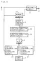
- FIG. 8 is a block diagram showing the configuration of a video signal processing apparatus according to a second embodiment of the invention.
- the synchronizing signal separation circuit 8 in the first embodiment shown in FIG. 6 is replaced by a vertical synchronizing signal separation circuit 24, the reset circuit 6 by a vertical-direction reset circuit 22, the counter circuit 7 by a vertical-direction counter circuit 23, and the synchronizing signal generating circuit 5 by a vertical synchronizing signal generating circuit 21; in other respects, the second embodiment is identical to the first embodiment, and description of the construction and operation of the other parts will not be repeated herein.
- the operation of the second embodiment is the same as that of the first embodiment.
- the circuit configuration is modified as stated above, there is no need to write the vertical retrace interval of the input video signal into the memory circuit 10, and consequently, the capacity of the memory circuit 10 can be reduced by that amount. More specifically, this embodiment achieves a saving of about 7.6% in the capacity of the memory circuit 10, as compared with the configuration that requires the whole input video signal to be stored in the memory circuit 10.
- FIG. 9 is a block diagram showing the configuration of a video signal processing apparatus according to a third embodiment of the invention.
- the synchronizing signal separation circuit 8 in the first embodiment shown in FIG. 6 is replaced by a horizontal synchronizing signal separation circuit 34, the reset circuit 6 by a horizontal-direction reset circuit 32, the counter circuit 7 by a horizontal-direction counter circuit 33, and the synchronizing signal generating circuit 5 by a horizontal synchronizing signal generating circuit 31; in other respects, the third embodiment is identical to the first embodiment, and description of the construction and operation of the other parts will not be repeated herein.
- the operation of the third embodiment is the same as that of the first embodiment.
- the third embodiment since the circuit configuration is modified as stated above, there is no need to write the horizontal retrace interval of the input video signal into the memory circuit 10, and consequently, the capacity of the memory circuit 10 can be further reduced as compared to the second embodiment. More specifically, the third embodiment achieves a saving of about 9.5% in the capacity of the memory circuit 10, as compared with the configuration that requires the whole input video signal to be stored in the memory circuit 10.
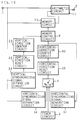
- FIG. 10 is a block diagram showing the configuration of a video signal processing apparatus according to a fourth embodiment of the invention.
- the configuration of the fourth embodiment shown in FIG. 10 is the same as that of the third embodiment shown in FIG. 9, except that the same vertical synchronizing signal separation circuit 24, vertical-direction reset circuit 22, and vertical-direction counter circuit 23 as those in the second embodiment shown in FIG. 8 are added. Description of the construction and operation of the other parts, therefore, will not be repeated herein.
- the portion of the video signal to be written into the memory circuit 10 can be specified in the vertical direction.
- the vertical retrace interval is not stored in the memory circuit 10, achieving a further saving in the capacity of the memory circuit 10 as compared with the third embodiment; that is, the fourth embodiment achieves a greater reduction in the capacity of the memory circuit 10 than any of the first, second, and third embodiments.
- the configuration of the present embodiment achieves a saving of about 16.4% in the capacity of the memory circuit 10, as compared with the configuration that requires the whole input video signal to be stored in the memory circuit 10.
- FIG. 11 is a block diagram showing the configuration of a video signal processing apparatus according to a fifth embodiment of the invention.
- the configuration of the fifth embodiment shown in FIG. 11 is identical to that of the first embodiment shown in FIG. 6, except that a video information extracting circuit 51 is added. Description of the construction and operation of the other parts, therefore, will not be repeated herein.
- the video information extracting circuit 51 is a circuit that extracts only the information necessary for the arithmetic operations in the arithmetic circuit 11. Generally, the extracted video information is smaller in data amount than the video signal before extraction. Therefore, by supplying the video information outputted from the video information extracting circuit 51 as input data to the memory circuit 10, the capacity of the memory circuit 10 can be further reduced in the first, second, third, and fourth embodiments.
- One specific application example of the fifth embodiment is a ghost eliminator that eliminates the ghost, a phenomenon caused by the reflection of the transmitted video signal.
- the video information extracting circuit 51 is configured as a gate circuit for extracting the signal superposed on the video signal for ghost elimination, and the arithmetic circuit 11 performs arithmetic operations to extract the transmission characteristic of the video signal transmission path.
- Another specific application example of the fifth embodiment is a noise suppressor that suppresses noise by performing arithmetic operations in the direction of time axis.
- the video signal information extracting circuit 51 extracts noise components over the entire screen, and the extracted noise components, not the video signal itself, are stored in the memory circuit 10.
- FIG. 12 is a block diagram showing the configuration of a video signal processing apparatus according to a sixth embodiment of the invention.
- the configuration of the sixth embodiment shown in FIG. 12 is identical to that of the first embodiment shown in FIG. 6, except that a standard video signal detection circuit 61 for controlling the timer circuit 3 is added. Description of the construction and operation of the other parts, therefore, will not be repeated herein.
- the input video signal switches to a non-standard video signal, and then switches back to the standard video signal.
- the operating cycle of the loop formed when the input terminal b is connected to the output terminal y in the switch circuit 4, that is, the cycle and phase of the synchronizing signal generating circuit 5, is synchronized with the input video signal, and the portion and position of the input video signal to be written into the memory circuit 10 are determined in accordance with the values preset by the memory control circuit 9.
- the standard video signal detection circuit 61 is provided to detect whether the input video signal is a standard signal or a non-standard signal, and using the result of the detection in the standard video signal detection circuit 61, the timer circuit 3 is controlled.
- the standard video signal detection circuit 61 supplies the resulting information to the timer circuit 3.
- the timer circuit 3 is put in the initial state. That is, the input terminal a is connected to the output terminal y in the switch circuit 4, and the operation is performed to achieve phase synchronization between the input video signal and the synchronizing signal outputted from the synchronizing signal separation circuit 8. The operation after that is the same as in the first embodiment.
Landscapes
- Engineering & Computer Science (AREA)
- Multimedia (AREA)
- Signal Processing (AREA)
- Television Signal Processing For Recording (AREA)
- Processing Of Color Television Signals (AREA)
- Synchronizing For Television (AREA)
Applications Claiming Priority (2)
| Application Number | Priority Date | Filing Date | Title |
|---|---|---|---|
| JP310464/93 | 1993-12-10 | ||
| JP31046493A JP3200658B2 (ja) | 1993-12-10 | 1993-12-10 | 映像信号処理装置及び映像信号記録・再生装置 |
Publications (3)
| Publication Number | Publication Date |
|---|---|
| EP0658046A2 true EP0658046A2 (de) | 1995-06-14 |
| EP0658046A3 EP0658046A3 (de) | 1995-11-15 |
| EP0658046B1 EP0658046B1 (de) | 1999-02-24 |
Family
ID=18005570
Family Applications (1)
| Application Number | Title | Priority Date | Filing Date |
|---|---|---|---|
| EP94118560A Expired - Lifetime EP0658046B1 (de) | 1993-12-10 | 1994-11-25 | Videosignalverarbeitungsgerät und -verfahren |
Country Status (4)
| Country | Link |
|---|---|
| US (1) | US5543854A (de) |
| EP (1) | EP0658046B1 (de) |
| JP (1) | JP3200658B2 (de) |
| DE (1) | DE69416649T2 (de) |
Cited By (2)
| Publication number | Priority date | Publication date | Assignee | Title |
|---|---|---|---|---|
| WO1998012873A1 (en) * | 1996-09-20 | 1998-03-26 | Thomson Consumer Electronics, Inc. | A delay correction circuit |
| US7599005B2 (en) | 2004-07-09 | 2009-10-06 | Sony Deutschland Gmbh | Method for synchronizing video signals |
Families Citing this family (4)
| Publication number | Priority date | Publication date | Assignee | Title |
|---|---|---|---|---|
| US6366327B1 (en) * | 1997-12-22 | 2002-04-02 | Texas Instruments Incorporated | Vertical sync detection and output for video decoder |
| US7173945B1 (en) | 2002-03-11 | 2007-02-06 | Cisco Technology, Inc. | Removing jitter by adaptive slope tracking |
| US7499446B1 (en) | 2002-04-29 | 2009-03-03 | Cisco Technology, Inc. | Removing jitter in RTP streaming media streams |
| US8121116B1 (en) | 2008-05-30 | 2012-02-21 | Cisco Technology, Inc. | Intra channel video stream scheduling |
Family Cites Families (9)
| Publication number | Priority date | Publication date | Assignee | Title |
|---|---|---|---|---|
| IT1099331B (it) * | 1977-09-26 | 1985-09-18 | Philips Nv | Complesso ricevitore per televisione |
| JPS592227B2 (ja) * | 1978-08-21 | 1984-01-17 | 株式会社日立製作所 | 雑音除去方式 |
| NL8005054A (nl) * | 1980-09-08 | 1982-04-01 | Philips Nv | Schakeling voor het opwekken van een periodiek zaagtandvormig signaal. |
| JPS57160286A (en) * | 1981-03-28 | 1982-10-02 | Sony Corp | Time base correcting device |
| NL8103437A (nl) * | 1981-07-21 | 1983-02-16 | Philips Nv | Synchroniseerschakeling voor een televisie-ontvanger. |
| CA1318972C (en) * | 1989-09-25 | 1993-06-08 | Alain Tessier | Video overlay circuit |
| DE69130097T2 (de) * | 1990-09-29 | 1999-02-25 | Canon K.K., Tokio/Tokyo | Vorrichtung zum Verarbeiten eines Bildsignals |
| GB9113922D0 (en) * | 1991-06-27 | 1991-08-14 | Thomson Consumer Electronics | Television sync disable circuit |
| US5281926A (en) * | 1992-10-06 | 1994-01-25 | Zenith Electronics Corp. | Phase locked loop made operative when stable input sync signal is detected |
-
1993
- 1993-12-10 JP JP31046493A patent/JP3200658B2/ja not_active Expired - Fee Related
-
1994
- 1994-11-25 DE DE69416649T patent/DE69416649T2/de not_active Expired - Fee Related
- 1994-11-25 EP EP94118560A patent/EP0658046B1/de not_active Expired - Lifetime
- 1994-12-08 US US08/355,160 patent/US5543854A/en not_active Expired - Fee Related
Cited By (2)
| Publication number | Priority date | Publication date | Assignee | Title |
|---|---|---|---|---|
| WO1998012873A1 (en) * | 1996-09-20 | 1998-03-26 | Thomson Consumer Electronics, Inc. | A delay correction circuit |
| US7599005B2 (en) | 2004-07-09 | 2009-10-06 | Sony Deutschland Gmbh | Method for synchronizing video signals |
Also Published As
| Publication number | Publication date |
|---|---|
| US5543854A (en) | 1996-08-06 |
| JP3200658B2 (ja) | 2001-08-20 |
| DE69416649T2 (de) | 1999-09-30 |
| DE69416649D1 (de) | 1999-04-01 |
| EP0658046A3 (de) | 1995-11-15 |
| JPH07162808A (ja) | 1995-06-23 |
| EP0658046B1 (de) | 1999-02-24 |
Similar Documents
| Publication | Publication Date | Title |
|---|---|---|
| KR940006625B1 (ko) | 비디오 신호 처리 시스템 | |
| US5734435A (en) | Video processing to convert between field rates | |
| JPS6053940B2 (ja) | フレ−ムシンクロナイザにおける書き込み禁止制御回路 | |
| US5543854A (en) | Video signal processing apparatus, video signal processing method, and video signal recording/reproduction apparatus | |
| JPH02305190A (ja) | テレビジョン受像機 | |
| JP3092938B2 (ja) | 画像表示装置用ディジタル同期回路 | |
| JP3935945B2 (ja) | 補助画像と主画像を合成する装置 | |
| US4984070A (en) | Picture quality improving apparatus capable of reducing deterioration of interpolated signal | |
| US5369498A (en) | Video disk player comprising a signal selection circuit for selecting one of a video data signal and a luminance signal as an output signal | |
| JP3299838B2 (ja) | ワイドアスペクトテレビジョン表示装置 | |
| EP0346980B1 (de) | Verfahren und Vorrichtung zur Aufzeichnung und Wiedergabe von Zwischenzeilensignalen | |
| JP3125270B2 (ja) | Pal信号のyc分離回路における動き検出回路、およびメモリ制御回路 | |
| EP0420184B1 (de) | Videosignalverarbeitungsschaltung | |
| KR0150961B1 (ko) | 문자자막정보장치의 레퍼런스신호 발생회로 | |
| JP3445297B2 (ja) | 多方式対応デジタルテレビジョン受信機 | |
| JP2624332B2 (ja) | Hdtv信号判別切換回路 | |
| JP2002010206A (ja) | 映像信号出力装置及び映像信号出力方法 | |
| JP2897277B2 (ja) | 映像信号制御装置 | |
| EP0849939A2 (de) | Bewegungsdetektionsschaltung und Speichersteuerungsschaltung in Y/C-Trennschaltung für PAL-Signale | |
| JP3140202B2 (ja) | ゴースト除去装置 | |
| JP3164075B2 (ja) | 映像信号処理回路 | |
| JP2992385B2 (ja) | 動き検出回路および映像記録再生装置 | |
| JP2614638B2 (ja) | ゴースト除去装置 | |
| JP2997013B2 (ja) | 垂直同期再生回路 | |
| JP2549673Y2 (ja) | 文字放送再生装置 |
Legal Events
| Date | Code | Title | Description |
|---|---|---|---|
| PUAI | Public reference made under article 153(3) epc to a published international application that has entered the european phase |
Free format text: ORIGINAL CODE: 0009012 |
|
| AK | Designated contracting states |
Kind code of ref document: A2 Designated state(s): DE GB NL |
|
| PUAL | Search report despatched |
Free format text: ORIGINAL CODE: 0009013 |
|
| AK | Designated contracting states |
Kind code of ref document: A3 Designated state(s): DE GB NL |
|
| 17P | Request for examination filed |
Effective date: 19951117 |
|
| 17Q | First examination report despatched |
Effective date: 19971013 |
|
| GRAG | Despatch of communication of intention to grant |
Free format text: ORIGINAL CODE: EPIDOS AGRA |
|
| GRAG | Despatch of communication of intention to grant |
Free format text: ORIGINAL CODE: EPIDOS AGRA |
|
| GRAH | Despatch of communication of intention to grant a patent |
Free format text: ORIGINAL CODE: EPIDOS IGRA |
|
| GRAH | Despatch of communication of intention to grant a patent |
Free format text: ORIGINAL CODE: EPIDOS IGRA |
|
| GRAA | (expected) grant |
Free format text: ORIGINAL CODE: 0009210 |
|
| AK | Designated contracting states |
Kind code of ref document: B1 Designated state(s): DE GB NL |
|
| REF | Corresponds to: |
Ref document number: 69416649 Country of ref document: DE Date of ref document: 19990401 |
|
| PLBE | No opposition filed within time limit |
Free format text: ORIGINAL CODE: 0009261 |
|
| STAA | Information on the status of an ep patent application or granted ep patent |
Free format text: STATUS: NO OPPOSITION FILED WITHIN TIME LIMIT |
|
| 26N | No opposition filed | ||
| REG | Reference to a national code |
Ref country code: GB Ref legal event code: 746 Effective date: 20010103 |
|
| REG | Reference to a national code |
Ref country code: GB Ref legal event code: IF02 |
|
| PGFP | Annual fee paid to national office [announced via postgrant information from national office to epo] |
Ref country code: GB Payment date: 20021120 Year of fee payment: 9 |
|
| PGFP | Annual fee paid to national office [announced via postgrant information from national office to epo] |
Ref country code: DE Payment date: 20021128 Year of fee payment: 9 |
|
| PGFP | Annual fee paid to national office [announced via postgrant information from national office to epo] |
Ref country code: NL Payment date: 20021129 Year of fee payment: 9 |
|
| PG25 | Lapsed in a contracting state [announced via postgrant information from national office to epo] |
Ref country code: GB Free format text: LAPSE BECAUSE OF NON-PAYMENT OF DUE FEES Effective date: 20031125 |
|
| PG25 | Lapsed in a contracting state [announced via postgrant information from national office to epo] |
Ref country code: NL Free format text: LAPSE BECAUSE OF NON-PAYMENT OF DUE FEES Effective date: 20040601 |
|
| PG25 | Lapsed in a contracting state [announced via postgrant information from national office to epo] |
Ref country code: DE Free format text: LAPSE BECAUSE OF NON-PAYMENT OF DUE FEES Effective date: 20040602 |
|
| GBPC | Gb: european patent ceased through non-payment of renewal fee |
Effective date: 20031125 |
|
| NLV4 | Nl: lapsed or anulled due to non-payment of the annual fee |
Effective date: 20040601 |