EP0658079A1 - Elektromagnetische Abschirmung durch Einkapselung für eine modular mehrfachige Logikhaupteinheit - Google Patents
Elektromagnetische Abschirmung durch Einkapselung für eine modular mehrfachige Logikhaupteinheit Download PDFInfo
- Publication number
- EP0658079A1 EP0658079A1 EP94119509A EP94119509A EP0658079A1 EP 0658079 A1 EP0658079 A1 EP 0658079A1 EP 94119509 A EP94119509 A EP 94119509A EP 94119509 A EP94119509 A EP 94119509A EP 0658079 A1 EP0658079 A1 EP 0658079A1
- Authority
- EP
- European Patent Office
- Prior art keywords
- logic board
- circuit
- layer
- integrated circuits
- layers
- Prior art date
- Legal status (The legal status is an assumption and is not a legal conclusion. Google has not performed a legal analysis and makes no representation as to the accuracy of the status listed.)
- Withdrawn
Links
Images


Classifications
-
- H—ELECTRICITY
- H05—ELECTRIC TECHNIQUES NOT OTHERWISE PROVIDED FOR
- H05K—PRINTED CIRCUITS; CASINGS OR CONSTRUCTIONAL DETAILS OF ELECTRIC APPARATUS; MANUFACTURE OF ASSEMBLAGES OF ELECTRICAL COMPONENTS
- H05K9/00—Screening of apparatus or components against electric or magnetic fields
- H05K9/0007—Casings
- H05K9/002—Casings with localised screening
- H05K9/0039—Galvanic coupling of ground layer on printed circuit board [PCB] to conductive casing
-
- G—PHYSICS
- G05—CONTROLLING; REGULATING
- G05B—CONTROL OR REGULATING SYSTEMS IN GENERAL; FUNCTIONAL ELEMENTS OF SUCH SYSTEMS; MONITORING OR TESTING ARRANGEMENTS FOR SUCH SYSTEMS OR ELEMENTS
- G05B19/00—Program-control systems
- G05B19/02—Program-control systems electric
- G05B19/04—Program control other than numerical control, i.e. in sequence controllers or logic controllers
- G05B19/042—Program control other than numerical control, i.e. in sequence controllers or logic controllers using digital processors
- G05B19/0428—Safety, monitoring
Definitions
- the present invention relates to electro-magnetic field (EMF) shielding and, more particularly, EMF shielding of the main logic board for a processing system, for example, a postage meter mailing machine and like systems.
- EMF electro-magnetic field
- an EMF shielding arrangement for a logic board having a plurality of integrated circuit units surface mounted to said logic board, characterised by, said logic board being a laminate of a plurality of circuit layers having a top circuit layerand a bottom circuit layer, said integrated circuit units being surface mounted to the top surface of said top circuit layer, said circuit layers and to said bottom circuit layers, electrical communication means for providing electrical communication perpendicularly between said circuit layers and on the surface of said respective layers to and from said integrated circuit units, said top circuit layer having a conductive material formed around said integrated circuits mounted to the top layer of said logic board, and a top cover composed of EMF shielding material fixably mounted to the logic board to enclose said integrated circuits mounted to the top layer of said logic board and having said conductive material in contiguous contact, said logic board having a plurality of buffers in bus communication with a coupler located outside of said top cover.
- a main logic board is comprised of a plurality of laminated circuit layers having the main system controller components being a microprocessor, a plurality of memory units and an application specific integrated circuit surface mounted to the top circuit board and a plurality of circuit components mounted to both the top and bottom layers having electrical communication being provided perpendicularly between the layers and on the surface of the respective layers.
- a plurality of buffers are mounted to one of the outer layers of the main board in communication to a coupler mounted to either the top or bottom layer board.
- a top cover and bottom cover are secured by a screw which extends through the top cover, laminate and bottom cover to threadably engage a nut.
- This arrangement encloses the microcontroller system and locates the laminate in-between the covers and such that perimeters of the top and bottom covers are in contiguous contact with respective conductive rings.
- the placement of the top cover locates the pin connector and communication buffers outside of the top cover.
- the microcontroller system is comprised of a microprocessor, static random access memory, ASIC, memory, non-volatile memories, optical read only memory and a number of system integrated circuit chips (IC).
- ASIC application specific integrated circuit
- Bus and control line communication between the microprocessor, ASIC, other IC's and memory units extends in a conventional manner through and between the laminate layers with the subsequently noted exceptions.
- the ASIC is in independent bus communication with the respective communication buffers which are, in turn, in independent bus communication with a respective portion of the pin connector.
- the respective communication bus lines allow the circuit layers to communicate with a number of resistors and like electronic analog components for proper signal handling.
- a microprocessor system is mounted to a laminated plate, generally indicated as 13.
- the laminated plate 13 has conductive rings 19 adhered to the top and bottom surfaces, respectively, and a pin connector 23 is mounted to the top surface of the mounting plate 13.
- a top cover 21 and bottom cover 25 are secured by a screw 27 and nut 29 to locate the laminated plate 13 in-between and in a manner such that the perimeters of the top and bottom covers 21 and 25 contact the respective conductive ring 19.
- top cover 21 locates the pin connector 23 outside of the cover and a plurality of communication buffers 50, 51, 52, 53, 54, 55 and 56 are mounted to the top surface of the laminated plate 13 between the top cover 21 and the pin connector 23 of the top surface of the laminated plate 13.
- a microprocessor system mounted to the first circuit layer of the laminated plate 13 within the top cover 21 and conductive ring 19 is a microprocessor system comprised of a microprocessor 30, static random access memory 34, ASIC 32, memory 35, non-volatile memories 38 and 40, optical read only memory 42 and a number of further system components' (not shown).
- FIG. 4 schematically represented is the bus communication between the microprocessor 30, ASIC 32, and memory units 34, 36, 38, 40 and 42.
- the ASIC 32 is in independent bus J, K, L, M, N, O and P communication with respective buffers 50, 51, 52, 53, 54, 55 and 56.
- buffers 50, 51, 52, 53, 54, 55 and 56 are in communication with respective portions of the pin connector 23 by a respective bus line 59.
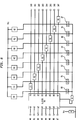
- the buffer 54 is illustrative also of buffers 50 to 56.
- a bus 59 communicates the output side of the buffer 54 to a plurality of pins IM0 to IM7 of the connector 23.
- the bus 59 is comprised of a plurality of lines 59a to 59h which connect at one end to the respective terminals IMO through IM7 of the pin connector 23 mounted on circuit layer 1 (Fig. 5).
- the bus lines 59a through 59h extends through circuit layer 1 to circuit layer 6 (Fig. 5) to respective resistors R1 surface mounted to the underside of circuit layer 6.
- the outputs of respective resistors R1 are directed from circuit layer 6 to circuit layer 1 and thence to the respective output pins B0 to B7 of the buffer 54.
- the buffer 54 has inputs A0 to A7 which inputs A0 to A7 are in line communication with a plurality of lines (M0 to M7) of the bus connected to ASIC 32.
- Each of the bus lines 59a to 59h has a respective resistor R2 in line communication with the one side of a respective resistor R1.
- the other side of each resistor R2 is in line communication with a reference voltage Vcc from Vcc layer 4.
- each of the bus lines 59a to 59h has a corresponding capacitor 60 to 67 in line communication with the one side of a respective resistor R1.
Landscapes
- Engineering & Computer Science (AREA)
- Microelectronics & Electronic Packaging (AREA)
- Physics & Mathematics (AREA)
- General Physics & Mathematics (AREA)
- Automation & Control Theory (AREA)
- Shielding Devices Or Components To Electric Or Magnetic Fields (AREA)
Applications Claiming Priority (2)
| Application Number | Priority Date | Filing Date | Title |
|---|---|---|---|
| US16377393A | 1993-12-09 | 1993-12-09 | |
| US163773 | 1993-12-09 |
Publications (1)
| Publication Number | Publication Date |
|---|---|
| EP0658079A1 true EP0658079A1 (de) | 1995-06-14 |
Family
ID=22591500
Family Applications (1)
| Application Number | Title | Priority Date | Filing Date |
|---|---|---|---|
| EP94119509A Withdrawn EP0658079A1 (de) | 1993-12-09 | 1994-12-09 | Elektromagnetische Abschirmung durch Einkapselung für eine modular mehrfachige Logikhaupteinheit |
Country Status (2)
| Country | Link |
|---|---|
| EP (1) | EP0658079A1 (de) |
| CA (1) | CA2137497A1 (de) |
Cited By (1)
| Publication number | Priority date | Publication date | Assignee | Title |
|---|---|---|---|---|
| EP0729294A1 (de) * | 1995-02-24 | 1996-08-28 | Hewlett-Packard Company | Vorrichtung zur Verhinderung elektromagnetischer Störung |
Citations (3)
| Publication number | Priority date | Publication date | Assignee | Title |
|---|---|---|---|---|
| JPS6472585A (en) * | 1987-09-11 | 1989-03-17 | Iwatsu Electric Co Ltd | Printed wiring board structure |
| WO1991006202A1 (en) * | 1989-10-13 | 1991-05-02 | Electricity Association Services Limited | Printed circuit board arrangement |
| EP0507018A1 (de) * | 1989-10-04 | 1992-10-07 | Pitney Bowes PLC | Gehäusestruktur |
-
1994
- 1994-12-07 CA CA 2137497 patent/CA2137497A1/en not_active Abandoned
- 1994-12-09 EP EP94119509A patent/EP0658079A1/de not_active Withdrawn
Patent Citations (3)
| Publication number | Priority date | Publication date | Assignee | Title |
|---|---|---|---|---|
| JPS6472585A (en) * | 1987-09-11 | 1989-03-17 | Iwatsu Electric Co Ltd | Printed wiring board structure |
| EP0507018A1 (de) * | 1989-10-04 | 1992-10-07 | Pitney Bowes PLC | Gehäusestruktur |
| WO1991006202A1 (en) * | 1989-10-13 | 1991-05-02 | Electricity Association Services Limited | Printed circuit board arrangement |
Non-Patent Citations (2)
| Title |
|---|
| A. S. SHUBAT: "A family of user-programmable peripherals with a functional unit architecture", IEEE JOURNAL OF SOLID-STATE CIRCUITS, vol. 27, no. 4, April 1992 (1992-04-01), NEW YORK US, pages 515 - 529, XP000296706 * |
| PATENT ABSTRACTS OF JAPAN vol. 13, no. 292 (E - 782) 6 July 1989 (1989-07-06) * |
Cited By (1)
| Publication number | Priority date | Publication date | Assignee | Title |
|---|---|---|---|---|
| EP0729294A1 (de) * | 1995-02-24 | 1996-08-28 | Hewlett-Packard Company | Vorrichtung zur Verhinderung elektromagnetischer Störung |
Also Published As
| Publication number | Publication date |
|---|---|
| CA2137497A1 (en) | 1995-06-10 |
Similar Documents
| Publication | Publication Date | Title |
|---|---|---|
| US4851685A (en) | Device for measuring UV-radiation | |
| US5841414A (en) | Liquid crystal display device | |
| JP2005505066A (ja) | ディスプレイ付きチップカード | |
| TW505803B (en) | Integrated circuit for driving liquid crystal | |
| JPS5987842A (ja) | Ic/lsiソケツト | |
| CN100364088C (zh) | 可编程电子处理器件的装置 | |
| JPS6216553A (ja) | 制御回路内蔵型電力半導体装置 | |
| CA2137497A1 (en) | Electro-magnetic field encapsulating shielding for a modular universal main logic board | |
| EP0225068A2 (de) | Elektronische Frankiermaschine | |
| US6472733B1 (en) | Electronic circuit support comprising tear resistant means | |
| US5654730A (en) | Liquid crystal display device | |
| JP4083381B2 (ja) | 遊技機 | |
| JPH05307520A (ja) | 二つの異なるマイクロプロセッサのいずれかで演算するためのデータ処理システム | |
| JPS58209158A (ja) | マスタスライス半導体装置 | |
| JPS57192058A (en) | Semiconductor device | |
| US20020179988A1 (en) | Pakage structure integrating image sensor to controller chip of scanning apparatus | |
| CA1241745A (en) | Magnetic bubble memory module | |
| JPH01112586A (ja) | 小型ディスク駆動機実装構造 | |
| JP2925030B2 (ja) | 制御基板ユニット | |
| JPH08161450A (ja) | カード状記憶装置 | |
| US4959555A (en) | Interconnection medium | |
| EP0768212A3 (de) | Steuerungsmodul | |
| US20050030147A1 (en) | Integrated connector and positive thermal coefficient switch | |
| JP2911288B2 (ja) | サーボモータの駆動用制御装置 | |
| JP2605040Y2 (ja) | Icのピン切替え回路 |
Legal Events
| Date | Code | Title | Description |
|---|---|---|---|
| PUAI | Public reference made under article 153(3) epc to a published international application that has entered the european phase |
Free format text: ORIGINAL CODE: 0009012 |
|
| AK | Designated contracting states |
Kind code of ref document: A1 Designated state(s): CH DE FR GB LI |
|
| RIN1 | Information on inventor provided before grant (corrected) |
Inventor name: PANTINO, RUSS R. Inventor name: PAGLIARO, PETER A. Inventor name: NAMBUDIRI, EASWARAN C.N. Inventor name: MULLER, ARNO |
|
| STAA | Information on the status of an ep patent application or granted ep patent |
Free format text: STATUS: THE APPLICATION HAS BEEN WITHDRAWN |
|
| 18W | Application withdrawn |
Withdrawal date: 19950920 |