EP0658969A2 - Elektrische Leistungsumwandlungsvorrichtung - Google Patents
Elektrische Leistungsumwandlungsvorrichtung Download PDFInfo
- Publication number
- EP0658969A2 EP0658969A2 EP94119530A EP94119530A EP0658969A2 EP 0658969 A2 EP0658969 A2 EP 0658969A2 EP 94119530 A EP94119530 A EP 94119530A EP 94119530 A EP94119530 A EP 94119530A EP 0658969 A2 EP0658969 A2 EP 0658969A2
- Authority
- EP
- European Patent Office
- Prior art keywords
- output voltage
- pulse
- mode
- generation means
- pulse generation
- Prior art date
- Legal status (The legal status is an assumption and is not a legal conclusion. Google has not performed a legal analysis and makes no representation as to the accuracy of the status listed.)
- Withdrawn
Links
- 238000006243 chemical reaction Methods 0.000 title description 3
- 238000010586 diagram Methods 0.000 description 17
- 230000001052 transient effect Effects 0.000 description 10
- 238000000034 method Methods 0.000 description 8
- 230000010349 pulsation Effects 0.000 description 6
- 230000001276 controlling effect Effects 0.000 description 5
- 238000013459 approach Methods 0.000 description 3
- 230000006698 induction Effects 0.000 description 3
- 239000003990 capacitor Substances 0.000 description 2
- 230000002411 adverse Effects 0.000 description 1
- 230000003466 anti-cipated effect Effects 0.000 description 1
- 230000015556 catabolic process Effects 0.000 description 1
- 230000007423 decrease Effects 0.000 description 1
- 230000000694 effects Effects 0.000 description 1
- 238000009499 grossing Methods 0.000 description 1
- 230000001105 regulatory effect Effects 0.000 description 1
Images


Classifications
-
- H—ELECTRICITY
- H02—GENERATION; CONVERSION OR DISTRIBUTION OF ELECTRIC POWER
- H02M—APPARATUS FOR CONVERSION BETWEEN AC AND AC, BETWEEN AC AND DC, OR BETWEEN DC AND DC, AND FOR USE WITH MAINS OR SIMILAR POWER SUPPLY SYSTEMS; CONVERSION OF DC OR AC INPUT POWER INTO SURGE OUTPUT POWER; CONTROL OR REGULATION THEREOF
- H02M7/00—Conversion of AC power input into DC power output; Conversion of DC power input into AC power output
- H02M7/42—Conversion of DC power input into AC power output without possibility of reversal
- H02M7/44—Conversion of DC power input into AC power output without possibility of reversal by static converters
- H02M7/48—Conversion of DC power input into AC power output without possibility of reversal by static converters using discharge tubes with control electrode or semiconductor devices with control electrode
- H02M7/505—Conversion of DC power input into AC power output without possibility of reversal by static converters using discharge tubes with control electrode or semiconductor devices with control electrode using devices of a thyratron or thyristor type requiring extinguishing means
- H02M7/515—Conversion of DC power input into AC power output without possibility of reversal by static converters using discharge tubes with control electrode or semiconductor devices with control electrode using devices of a thyratron or thyristor type requiring extinguishing means using semiconductor devices only
- H02M7/525—Conversion of DC power input into AC power output without possibility of reversal by static converters using discharge tubes with control electrode or semiconductor devices with control electrode using devices of a thyratron or thyristor type requiring extinguishing means using semiconductor devices only with automatic control of output waveform or frequency
- H02M7/527—Conversion of DC power input into AC power output without possibility of reversal by static converters using discharge tubes with control electrode or semiconductor devices with control electrode using devices of a thyratron or thyristor type requiring extinguishing means using semiconductor devices only with automatic control of output waveform or frequency by pulse width modulation
-
- H—ELECTRICITY
- H02—GENERATION; CONVERSION OR DISTRIBUTION OF ELECTRIC POWER
- H02M—APPARATUS FOR CONVERSION BETWEEN AC AND AC, BETWEEN AC AND DC, OR BETWEEN DC AND DC, AND FOR USE WITH MAINS OR SIMILAR POWER SUPPLY SYSTEMS; CONVERSION OF DC OR AC INPUT POWER INTO SURGE OUTPUT POWER; CONTROL OR REGULATION THEREOF
- H02M7/00—Conversion of AC power input into DC power output; Conversion of DC power input into AC power output
- H02M7/42—Conversion of DC power input into AC power output without possibility of reversal
- H02M7/44—Conversion of DC power input into AC power output without possibility of reversal by static converters
- H02M7/48—Conversion of DC power input into AC power output without possibility of reversal by static converters using discharge tubes with control electrode or semiconductor devices with control electrode
- H02M7/53—Conversion of DC power input into AC power output without possibility of reversal by static converters using discharge tubes with control electrode or semiconductor devices with control electrode using devices of a triode or transistor type requiring continuous application of a control signal
- H02M7/537—Conversion of DC power input into AC power output without possibility of reversal by static converters using discharge tubes with control electrode or semiconductor devices with control electrode using devices of a triode or transistor type requiring continuous application of a control signal using semiconductor devices only, e.g. single switched pulse inverters
- H02M7/539—Conversion of DC power input into AC power output without possibility of reversal by static converters using discharge tubes with control electrode or semiconductor devices with control electrode using devices of a triode or transistor type requiring continuous application of a control signal using semiconductor devices only, e.g. single switched pulse inverters with automatic control of output wave form or frequency
- H02M7/5395—Conversion of DC power input into AC power output without possibility of reversal by static converters using discharge tubes with control electrode or semiconductor devices with control electrode using devices of a triode or transistor type requiring continuous application of a control signal using semiconductor devices only, e.g. single switched pulse inverters with automatic control of output wave form or frequency by pulse-width modulation
-
- H—ELECTRICITY
- H02—GENERATION; CONVERSION OR DISTRIBUTION OF ELECTRIC POWER
- H02M—APPARATUS FOR CONVERSION BETWEEN AC AND AC, BETWEEN AC AND DC, OR BETWEEN DC AND DC, AND FOR USE WITH MAINS OR SIMILAR POWER SUPPLY SYSTEMS; CONVERSION OF DC OR AC INPUT POWER INTO SURGE OUTPUT POWER; CONTROL OR REGULATION THEREOF
- H02M1/00—Details of apparatus for conversion
- H02M1/08—Circuits specially adapted for the generation of control voltages for semiconductor devices incorporated in static converters
-
- H—ELECTRICITY
- H02—GENERATION; CONVERSION OR DISTRIBUTION OF ELECTRIC POWER
- H02M—APPARATUS FOR CONVERSION BETWEEN AC AND AC, BETWEEN AC AND DC, OR BETWEEN DC AND DC, AND FOR USE WITH MAINS OR SIMILAR POWER SUPPLY SYSTEMS; CONVERSION OF DC OR AC INPUT POWER INTO SURGE OUTPUT POWER; CONTROL OR REGULATION THEREOF
- H02M7/00—Conversion of AC power input into DC power output; Conversion of DC power input into AC power output
- H02M7/42—Conversion of DC power input into AC power output without possibility of reversal
- H02M7/44—Conversion of DC power input into AC power output without possibility of reversal by static converters
- H02M7/48—Conversion of DC power input into AC power output without possibility of reversal by static converters using discharge tubes with control electrode or semiconductor devices with control electrode
- H02M7/53—Conversion of DC power input into AC power output without possibility of reversal by static converters using discharge tubes with control electrode or semiconductor devices with control electrode using devices of a triode or transistor type requiring continuous application of a control signal
- H02M7/537—Conversion of DC power input into AC power output without possibility of reversal by static converters using discharge tubes with control electrode or semiconductor devices with control electrode using devices of a triode or transistor type requiring continuous application of a control signal using semiconductor devices only, e.g. single switched pulse inverters
- H02M7/5387—Conversion of DC power input into AC power output without possibility of reversal by static converters using discharge tubes with control electrode or semiconductor devices with control electrode using devices of a triode or transistor type requiring continuous application of a control signal using semiconductor devices only, e.g. single switched pulse inverters in a bridge configuration
- H02M7/53871—Conversion of DC power input into AC power output without possibility of reversal by static converters using discharge tubes with control electrode or semiconductor devices with control electrode using devices of a triode or transistor type requiring continuous application of a control signal using semiconductor devices only, e.g. single switched pulse inverters in a bridge configuration with automatic control of output voltage or current
- H02M7/53875—Conversion of DC power input into AC power output without possibility of reversal by static converters using discharge tubes with control electrode or semiconductor devices with control electrode using devices of a triode or transistor type requiring continuous application of a control signal using semiconductor devices only, e.g. single switched pulse inverters in a bridge configuration with automatic control of output voltage or current with analogue control of three-phase output
Definitions
- This invention relates to power conversion equipment which converts a direct current into an alternating current or vice versa, and in particular it relates to controlling of a pulse width modulation (PWM) inverter.
- PWM pulse width modulation
- a constant control is provided to maintain a constant ratio between a magnitude of an output voltage and a fundamental frequency in such a region where an output voltage fundamental frequency is low, which region will be referred to as a variable-voltage variable-frequency region, whereas a frequency control is provided while maintaining a maximum voltage value in such a region where the output voltage fundamental frequency increases such that the magnitude of its output voltage becomes a maximum, which region will be referred to as a constant-voltage variable-frequency region. Since in the variable-voltage variable-frequency region an output voltage is regulated by pulse width modulation control, a multi-pulse mode is utilized in which a half cycle of its output voltage comprises a plurality of voltage pulses. On the other hand, in the constant voltage variable-frequency region, in order to maximize its voltage usage rate to minimize the size of the equipment, a one-pulse mode is utilized in which a half cycle of its output voltage comprises a single broad pulse.
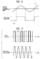
- a prior art inverter which uses GTO thyristors as its switching elements which will be referred to as a GTO inverter hereinafter, has adopted a multi-pulse mode according to a pulse count switching method which decrements by switching the number of pulses to be included in one cycle thereof with an increasing output voltage fundamental frequency as shown in Fig. 3. This is due to an upper limitation of several hundred Hz imposed on a switching frequency in the GTO thyristor. This method, however, involves such a problem that a magnetic noise which accompanies tone variation occurs thereby generating a cacophonic noise due to discontinuity between switching frequencies at the time the pulse count switching is employed.
- the main object of the invention is to provide a two-level inverter apparatus which is capable of controlling a magnitude of its output voltage from zero to a maximum value through combination of a multi-pulse mode and a one-pulse mode, wherein the discontinuity between the switching frequencies is substantially eliminated thereby reducing the cacophonic magnetic noise accompanying tone variations, as well as that a continuous control substantially over the entire region of the output voltage is enabled through minimization of a gap in the output voltages between the multi-pulse mode and the one-pulse mode.
- a multi-pulse generator means for generating a gate control signal for outputting a bipolar modulation voltage which is controlled by a pulse width modulation having a uniform pulse generation cycle over any cycle of its output voltage fundamental wave, and a gate control signal for outputting an overmodulation voltage the pulse width of which in the vicinity of a peak of the output voltage fundamental wave is widened than that in the vicinity of a zero cross point thereof; a one-pulse generation means for generating a single pulse having the same polarity as that of the output voltage fundamental wave; and a selection means for selecting either one of the outputs from the multi-pulse generation means and the one pulse generation means in dependence on a condition of the number of pulses contained in one cycle of the output fundamental wave, a magnitude of an output voltage, a modulation ratio, or an output voltage fundamental frequency.
- the multi-pulse generation means By arranging the multi-pulse generation means such that a pulse generation cycle of a pulse width modulated portion on an output voltage waveform is adapted to be set independently of the output voltage fundamental frequency, it becomes possible that its switching frequency at the time of bipolar modulation becomes constant, and that its switching frequency at the time of overmodulation is caused gradually to approach a predetermined switching frequency set for at the time of one-pulse, thereby eliminating discontinuity between switching frequencies.
- FIG. 4 A schematic diagram indicative of a PWM mode of inverter operation according to the invention is shown in Fig. 4.
- the inverter is operated in such a manner that it is operated in a bipolar mode in its low output voltage range, in an overmodulation mode in its high output voltage range, and in one pulse mode in its maximum output voltage range respectively.
- Fig. 1 is a schematic diagram illustrative of one embodiment of the invention, where numeral 6 is an induction motor, 5 is a two-level three-phase PWM inverter which drives the induction motor, 9 is an inverter power source from an aerial direct current feeder, and 7, 8 denote respectively a filter reactor and a capacitor provided on the DC input side of the inverter.
- a multi-pulse generation means 2 a one-pulse generation means 3 and a PWM mode select means 4 respectively generate inverter control signals on the basis of an output voltage command E* of the inverter and an output voltage fundamental wave phase ⁇ x of each phase which is obtained by integrating its frequency command Fi* in an integrator 1 (where suffix x represents any phase of u, v, w).
- S1 x , S2 x and S x are called a switching function which is defined to take 1 when the positive arm of the inverter is ON, and take O when the negative arm thereof is ON.
- An example of the multi-pulse generation means 2 is shown in Fig. 5 which indicates only one phase component of its contents.
- switching functions in the bipolar mode and the overmodulation mode are generated by the same generating means.
- An output voltage command-to-modulation ratio conversion means 21 obtains a modulation ratio A, that is, amplitude of a modulation wave, from an output voltage command E*.
- a carrier amplitude Assuming a carrier amplitude to be 1, the ratio becomes such that 0 ⁇ A ⁇ 1 in the bipolar mode, and that A>1 in the overmodulation mode.
- E* and A are adapted to correspond to equation 1 in the bipolar mode, and to equation 2 in the overmodulation mode.
- the switching function computing means 24 generates a carrier of triangular pulses having an amplitude of 1 and a frequency of Fc, which is compared with a value of the modulation wave to generate a switching function.
- the switching function may be obtained without using such triangular pulses through computation of the modulation wave a x and its pulse intervals.
- Figs. 6 and 7 show examples of waveforms of the switching functions according to the bipolar mode and the overmodulation mode obtained through comparison with the triangular pulses.
- IGBT inverter In the inverter equipment according to the present invention, devices such as IGBTs, large capacity transistors or the like which can be operated at switching frequencies of several kHz are utilized as a switching element (hereinafter referred to as an IGBT inverter in general), and the modulation wave and the carrier are arranged to be asynchronous in the multi-pulse mode operation. Thereby, its switching frequency is adapted to be constant in the bipolar mode, and to gradually approach a predetermined switching frequency in the one pulse mode which will be described later.
- the carrier Since the modulation wave and the carrier wave are asynchronous in the multi-pulse mode, it is necessary for the carrier to have a substantially higher frequency than the modulation frequency, preferably to have an approximately ten times higher frequency according to the experiences.
- FIG. 8 An example of a waveform of switching function which is generated by the one pulse generation means of Fig. 1 is shown in Fig. 8.
- a sign of the fundamental wave of output voltage is positive, irrespective of its amplitude, a value of switching function S2 x is adapted to be 1, and when the sign is negative the value of S2 x is adapted to be 0.
- a first problem is that a changing point at which the overmodulation mode is changed to the one pulse mode depends on its switching frequency, thereby, it cannot be set at discretion.
- a second problem is that in the case where a modulation wave and a carrier wave are asynchronous in the overmodulation mode, it occurs that pulses of modulation wave in the vicinity of zero-cross point thereof may be or not be generated in the vicinity of a border between the overmodulation mode and the one-pulse mode due to the influence of turn-on and turn-off time of the devices. As a result, there occurs unbalance between the positive and the negative output voltages, thereby causing a beat phenomenon to be introduced by which a low frequency pulsation is superimposed on a load current of the inverter.
- an output voltage waveform (which is equivalent to the waveform of a switching function to be described later) can be divided into two portions: one having a uniform pulse interval (equi-distance pulse), that is, having a uniform pulse generation cycle in the vicinity of the zero cross of the modulation wave; and the other portion having a single broad pulse width component with its center corresponding to a peak of the modulation wave, thereby, it is anticipated that a switch-over from the overmodulation mode to the one-pulse mode may occur in any portion having an equidistance pulse in the overmodulation mode.
- a load current in the inverter is fluctuated, which may result in a breakdown of switching elements due to overcurrents or in a substantial fluctuation in a torque generated by the inverter motor.
- a shift voltage at which a shift between the overmodulation and the one-pulse mode is allowed
- a shift phase a particular phase in the output voltage fundamental wave at which the shift should be executed.
- the shift voltage for performing shifting between the overmodulation mode and the one-pulse mode thereat is set at a value in close proximity of the output voltage in the one-pulse mode operation, that is, in proximity of 100 % because that a fluctuation in torque that the motor generates during mode shifting can be minimized when a difference of its output voltage from its maximum value available is minimum.
- FIG. 10 there is shown an example of relations between an average pulse number in the vicinity of zero cross point of the output voltage fundamental wave and a current pulsation due to the beat phenomenon.
- a portion of the modulation wave where its absolute value is under 1.0 corresponds to an equidistance pulse region as shown in Fig. 7, thereby, an average pulse number can be obtained by equation 3.
- the current pulsation ratio is defined by equation 4. It is shown by Fig. 10 that unless at least one pulse is secured in the vicinity of zero cross point of the output voltage fundamental wave, the low frequency pulsation in the inverter load current due to the beat phenomenon becomes extremely great.
- an appropriate shift voltage is preferably set at a value which ensures at least one voltage pulse in the vicinity of the zero cross point of the output voltage fundamental wave. Since this value depends on the output fundamental frequency Fi* and the carrier frequency Fc in the multi-pulse mode, there may be provided a means for obtaining this value from calculation of these values, or this value may be calculated and preset beforehand from an upper limit of the output voltage fundamental frequency Fi*.
- Fig. 11(a) shows a case where all the three phases were changed in batch at 0° of U-phase of the output voltage fundamental wave as illustrated in Fig. 12, and where a transient current fluctuation was observed immediately after mode changing.
- Fig. 11(b) shows another case where all the three phases were changed in batch at 90° of U-phase of the output voltage fundamental wave as illustrated in Fig. 13, and where there was observed almost no transient current fluctuation.
- Fig. 14 there is shown an example of relationships between the shift phase (U-phase taken as a reference) of the output voltage fundamental wave when shifting all the three phases in batch from the overmodulation mode to the one-pulse mode and the transient current fluctuation, where the current fluctuation rate is defined by equation 5.
- (current fluctuation rate) [(transient peak current at mode change)-(peak steady current in one-pulse mode)]/[(peak steady current in one-pulse mode)] x 100 (%) eq. 5
- Fig. 14 at every 60° of phase of the output voltage fundamental wave a large current fluctuation rate appears.
- a shift voltage in order to allow a batch mode change for the three phases to be executed between the overmodulation and the one-pulse mode, a shift voltage must be set at a value which is greater than 95.6%, and has at least one voltage pulse in the vicinity of the zero cross point of the output voltage fundamental wave in the overmodulation mode.
- a mode select command generation means 42 compares a shift voltage Ec set in a shift voltage means 41 and a voltage command E*, and outputs a mode select command Mc indicative of which one to select of the multipulse mode and the one-pulse mode.
- the mode select command Mc has been described hereinabove that it is obtained on the basis of the output voltage command E*, however, since the output voltage command E* univocally corresponds to the modulation ratio A, it may be arranged such that a particular modulation ratio Ac corresponding to the shift voltage is preset, which is then compared with the modulation ratio A to generate the mode select command Mc.
- variable voltage variable frequency region since the output voltage command and the output voltage fundamental frequency univocally correspond each other, it may be arranged such that a particular output voltage fundamental frequency Fic which corresponds to the shift voltage may be preset beforehand, which is then compared with the frequency command Fi* to generate the mode select command Mc.
- mode select switches 45, 46, 47 select either one of output S1x of the multipulse generation means and output S2x of the one-pulse generation means, then determine its switching function Sx.
- the shift phase may also be controlled in manner such that by taking absolute values of the modulation wave at respective phases, and if they all exceed 1.0, since which indicates that all the three phases lie in a wide pulse region in the overmodulation mode, a change of output from between the multipulse generation means and the one-pulse generation means is enabled at this instance.
- the two-level inverter equipment which features such advantages that a gap in the output voltages at the time of mode change between the multipulse mode and the one-pulse mode can be reduced as small as 1-2 % in comparison with approximately 10 % in the conventional GTO inverter, thereby allowing a continuous control of the output voltage from zero to its maximum value, and that a smooth change can be ensured between the multipulse mode and the one-pulse mode operation without causing any fluctuations in the current and the generated torque.
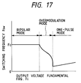
- Fig. 17 With reference to Fig. 17 there is shown a relation between the output voltage fundamental frequency and the switching frequency, where there exist no such large discontinuities as observed in Fig. 3 indicative of the conventional inverter modulation method, thereby eliminating the discontinuous tone change occurring due to the magnetic noise.
- inverter equipment which is capable of controlling its output voltage from zero to a maximum voltage by use of the multi-pulse mode and the one-pulse mode in conjunction according to the invention, discontinuous changes in the magnetically-induced noise can be eliminated, and a substantially continuous control over the full range of its output voltage can be accomplished as well.
Landscapes
- Engineering & Computer Science (AREA)
- Power Engineering (AREA)
- Inverter Devices (AREA)
Applications Claiming Priority (2)
| Application Number | Priority Date | Filing Date | Title |
|---|---|---|---|
| JP317702/93 | 1993-12-17 | ||
| JP31770293 | 1993-12-17 |
Publications (2)
| Publication Number | Publication Date |
|---|---|
| EP0658969A2 true EP0658969A2 (de) | 1995-06-21 |
| EP0658969A3 EP0658969A3 (de) | 1995-09-06 |
Family
ID=18091079
Family Applications (1)
| Application Number | Title | Priority Date | Filing Date |
|---|---|---|---|
| EP94119530A Withdrawn EP0658969A3 (de) | 1993-12-17 | 1994-12-09 | Elektrische Leistungsumwandlungsvorrichtung. |
Country Status (6)
| Country | Link |
|---|---|
| US (1) | US5680299A (de) |
| EP (1) | EP0658969A3 (de) |
| KR (1) | KR950022005A (de) |
| CN (1) | CN1036625C (de) |
| AU (1) | AU672538B2 (de) |
| ZA (1) | ZA949795B (de) |
Cited By (4)
| Publication number | Priority date | Publication date | Assignee | Title |
|---|---|---|---|---|
| EP0808016A1 (de) * | 1996-05-14 | 1997-11-19 | Hitachi, Ltd. | Pulsbreitenmodulierte Wechselrichter-Einrichtung |
| ES2292370A1 (es) * | 2007-07-13 | 2008-03-01 | Universidad Politecnica De Madrid | Fuente de alimentacion de alta tension para magnetrones de corriente continua y su modo de funcionamiento. |
| RU2460114C1 (ru) * | 2011-07-22 | 2012-08-27 | Федеральное Государственное Автономное Образовательное Учреждение Высшего Профессионального Образования "Сибирский Федеральный Университет" (Сфу) | Способ управления импульсным стабилизатором напряжения |
| WO2019145068A1 (de) * | 2018-01-24 | 2019-08-01 | Robert Bosch Gmbh | Verfahren und vorrichtung zum betreiben einer mehrphasigen elektrischen maschine |
Families Citing this family (21)
| Publication number | Priority date | Publication date | Assignee | Title |
|---|---|---|---|---|
| JP3346223B2 (ja) * | 1997-06-10 | 2002-11-18 | 株式会社日立製作所 | モータ制御方法及びモータ制御システム |
| US6307759B1 (en) * | 1997-10-31 | 2001-10-23 | Hitachi, Ltd. | Control device for electric power translating device |
| KR100332580B1 (ko) * | 2000-07-10 | 2002-04-15 | 차 동 해 | 짝수 레벨 인버터 |
| RU2007149319A (ru) * | 2005-05-27 | 2009-07-10 | Сименс Энерджи Энд Отомейшн, Инк. (Us) | Функционирование инверторов с перемодуляцией |
| CN101529714B (zh) * | 2006-10-19 | 2012-11-21 | 三菱电机株式会社 | 永磁同步电动机的矢量控制装置 |
| US8086355B1 (en) | 2007-02-28 | 2011-12-27 | Global Embedded Technologies, Inc. | Method, a system, a computer-readable medium, and a power controlling apparatus for applying and distributing power |
| JP2009240087A (ja) * | 2008-03-27 | 2009-10-15 | Hitachi Ltd | 回転電機の制御装置 |
| JP4858597B2 (ja) * | 2008-11-28 | 2012-01-18 | 株式会社デンソー | 回転機の制御装置及びその製造方法 |
| JP5116785B2 (ja) * | 2010-02-25 | 2013-01-09 | 株式会社日立製作所 | 交流電動機の駆動装置及び電動機車両 |
| RU2451973C1 (ru) * | 2011-02-25 | 2012-05-27 | Открытое акционерное общество "Концерн "Созвездие" | Стабилизатор постоянного напряжения |
| CN102223096B (zh) * | 2011-06-24 | 2013-09-18 | 株洲南车时代电气股份有限公司 | 一种双电平逆变器死区效应仿真建模装置及其方法 |
| KR20140060550A (ko) | 2011-09-30 | 2014-05-20 | 미쓰비시덴키 가부시키가이샤 | 전동기의 제어 장치 및 제어 방법, 그것들을 적용한 전동기 및 차량 구동 시스템 |
| MX2014003616A (es) * | 2011-09-30 | 2014-06-05 | Mitsubishi Electric Corp | Dispositivo de control de conversion de energia, metodo de control de conversion de energia, motor electrico, y sistema de accionamiento de vehiculo. |
| JP5503810B2 (ja) * | 2011-09-30 | 2014-05-28 | 三菱電機株式会社 | 電動機のベクトル制御装置、車両駆動システム |
| JP5929080B2 (ja) * | 2011-09-30 | 2016-06-01 | ダイキン工業株式会社 | 電力変換装置 |
| US9647575B2 (en) * | 2013-04-23 | 2017-05-09 | Mitsubishi Electric Corporation | Power converter |
| KR20150019187A (ko) * | 2013-08-13 | 2015-02-25 | 현대모비스 주식회사 | 차량 전원 공급 장치 |
| WO2016031030A1 (ja) | 2014-08-28 | 2016-03-03 | 三菱電機株式会社 | 電力変換装置および車両駆動システム |
| US9923484B2 (en) * | 2014-10-31 | 2018-03-20 | Ecole De Technologie Superieure | Method and system for operating a multilevel electric power inverter |
| DE102020200244A1 (de) * | 2020-01-10 | 2021-07-15 | Zf Friedrichshafen Ag | Zufälliges Verschieben von Schaltflanken eines Umrichterpulsmusters |
| CN118039442A (zh) * | 2023-12-04 | 2024-05-14 | 深圳市恒运昌真空技术股份有限公司 | 一种射频电源的多脉冲驱动方法 |
Family Cites Families (4)
| Publication number | Priority date | Publication date | Assignee | Title |
|---|---|---|---|---|
| JPS62163589A (ja) * | 1986-01-13 | 1987-07-20 | Hitachi Ltd | パルス幅変調インバ−タによる誘導電動機の制御装置 |
| JP2884880B2 (ja) * | 1992-02-12 | 1999-04-19 | 株式会社日立製作所 | 電力変換器の制御装置 |
| AU651034B2 (en) * | 1992-04-24 | 1994-07-07 | Hitachi Limited | Power converter for converting DC voltage into AC phase voltage having three levels of positive, zero and negative voltage |
| JP2814837B2 (ja) * | 1992-06-04 | 1998-10-27 | 株式会社日立製作所 | 電力変換装置 |
-
1994
- 1994-12-08 ZA ZA949795A patent/ZA949795B/xx unknown
- 1994-12-09 EP EP94119530A patent/EP0658969A3/de not_active Withdrawn
- 1994-12-13 AU AU80381/94A patent/AU672538B2/en not_active Expired
- 1994-12-15 KR KR1019940034391A patent/KR950022005A/ko not_active Withdrawn
- 1994-12-17 CN CN94119598A patent/CN1036625C/zh not_active Expired - Lifetime
- 1994-12-19 US US08/359,182 patent/US5680299A/en not_active Expired - Lifetime
Cited By (5)
| Publication number | Priority date | Publication date | Assignee | Title |
|---|---|---|---|---|
| EP0808016A1 (de) * | 1996-05-14 | 1997-11-19 | Hitachi, Ltd. | Pulsbreitenmodulierte Wechselrichter-Einrichtung |
| ES2292370A1 (es) * | 2007-07-13 | 2008-03-01 | Universidad Politecnica De Madrid | Fuente de alimentacion de alta tension para magnetrones de corriente continua y su modo de funcionamiento. |
| RU2460114C1 (ru) * | 2011-07-22 | 2012-08-27 | Федеральное Государственное Автономное Образовательное Учреждение Высшего Профессионального Образования "Сибирский Федеральный Университет" (Сфу) | Способ управления импульсным стабилизатором напряжения |
| WO2019145068A1 (de) * | 2018-01-24 | 2019-08-01 | Robert Bosch Gmbh | Verfahren und vorrichtung zum betreiben einer mehrphasigen elektrischen maschine |
| US11101743B2 (en) | 2018-01-24 | 2021-08-24 | Robert Bosch Gmbh | Method and device for operating a multi-phase electric machine |
Also Published As
| Publication number | Publication date |
|---|---|
| US5680299A (en) | 1997-10-21 |
| AU672538B2 (en) | 1996-10-03 |
| ZA949795B (en) | 1995-08-18 |
| EP0658969A3 (de) | 1995-09-06 |
| AU8038194A (en) | 1995-06-29 |
| CN1036625C (zh) | 1997-12-03 |
| KR950022005A (ko) | 1995-07-26 |
| CN1108443A (zh) | 1995-09-13 |
Similar Documents
| Publication | Publication Date | Title |
|---|---|---|
| EP0658969A2 (de) | Elektrische Leistungsumwandlungsvorrichtung | |
| EP0571755B1 (de) | Leistungswandler zur Umwandlung einer Gleichspannung in eine Dreistufenwechselspannung, die eine positive, eine null- und eine negative Spannung aufweist | |
| EP0597132B1 (de) | Leistungswandler | |
| EP0229656B1 (de) | Steuerverfahren für Impulsbreitenmodulationswechselrichter | |
| EP0358225B1 (de) | Leistungsumwandlungseinrichtung mit Schwebungsunterdrückung | |
| US6023417A (en) | Generalized discontinuous pulse width modulator | |
| US5375050A (en) | Electric power converter arrangement and electric rolling stock control device using the same | |
| JP6610804B2 (ja) | インバータの制御方法、制御装置及びインバータ | |
| JPS63287397A (ja) | 誘導電動機の制御装置 | |
| EP4092900A1 (de) | System zur steuerung einer elektrischen rotationsmaschine | |
| JP3455788B2 (ja) | 電力変換装置 | |
| EP0600635A2 (de) | Mehrfachwechselrichtersystem mit parallel-geschalteten Einheiten und Steuerverfahren dafür | |
| JP3700019B2 (ja) | 電気車の制御装置 | |
| JP3755089B2 (ja) | 電気車の制御装置 | |
| JP3826363B2 (ja) | 電気車の制御装置 | |
| JP2923727B2 (ja) | 電力変換装置 | |
| JP3747259B2 (ja) | 電気車の制御装置 | |
| JP3760248B2 (ja) | 電気車の制御装置 | |
| JP3873221B2 (ja) | 電気車の制御装置 | |
| JP3463169B2 (ja) | 電力変換装置 | |
| JP2003180079A (ja) | 中性点クランプ式電力変換装置 | |
| JP4277360B2 (ja) | 3レベルインバータの制御装置 | |
| JPH09163755A (ja) | 電力変換装置の制御装置 | |
| JP3411995B2 (ja) | 電力変換装置 | |
| JP3061957B2 (ja) | 中性点クランプ式インバータの制御装置 |
Legal Events
| Date | Code | Title | Description |
|---|---|---|---|
| PUAI | Public reference made under article 153(3) epc to a published international application that has entered the european phase |
Free format text: ORIGINAL CODE: 0009012 |
|
| AK | Designated contracting states |
Kind code of ref document: A2 Designated state(s): DE FR GB |
|
| PUAL | Search report despatched |
Free format text: ORIGINAL CODE: 0009013 |
|
| AK | Designated contracting states |
Kind code of ref document: A3 Designated state(s): DE FR GB |
|
| 17P | Request for examination filed |
Effective date: 19960222 |
|
| 17Q | First examination report despatched |
Effective date: 19990111 |
|
| STAA | Information on the status of an ep patent application or granted ep patent |
Free format text: STATUS: THE APPLICATION IS DEEMED TO BE WITHDRAWN |
|
| 18D | Application deemed to be withdrawn |
Effective date: 19990522 |