EP0659013A2 - Procédé et dispositif pour balayer un objet - Google Patents
Procédé et dispositif pour balayer un objet Download PDFInfo
- Publication number
- EP0659013A2 EP0659013A2 EP94307335A EP94307335A EP0659013A2 EP 0659013 A2 EP0659013 A2 EP 0659013A2 EP 94307335 A EP94307335 A EP 94307335A EP 94307335 A EP94307335 A EP 94307335A EP 0659013 A2 EP0659013 A2 EP 0659013A2
- Authority
- EP
- European Patent Office
- Prior art keywords
- light
- light sensor
- data
- image data
- illumination
- Prior art date
- Legal status (The legal status is an assumption and is not a legal conclusion. Google has not performed a legal analysis and makes no representation as to the accuracy of the status listed.)
- Withdrawn
Links
- 238000000034 method Methods 0.000 title claims abstract description 10
- 238000005286 illumination Methods 0.000 claims abstract description 32
- 230000035945 sensitivity Effects 0.000 claims description 5
- 239000013307 optical fiber Substances 0.000 description 8
- 238000010586 diagram Methods 0.000 description 6
- 230000002238 attenuated effect Effects 0.000 description 5
- 238000005259 measurement Methods 0.000 description 3
- 230000000712 assembly Effects 0.000 description 2
- 238000000429 assembly Methods 0.000 description 2
- 238000003384 imaging method Methods 0.000 description 2
- 239000000203 mixture Substances 0.000 description 2
- 230000004044 response Effects 0.000 description 2
- 230000032683 aging Effects 0.000 description 1
- 230000003247 decreasing effect Effects 0.000 description 1
- 239000006185 dispersion Substances 0.000 description 1
- 230000007613 environmental effect Effects 0.000 description 1
- 239000000835 fiber Substances 0.000 description 1
- 230000002431 foraging effect Effects 0.000 description 1
- 230000010355 oscillation Effects 0.000 description 1
- 238000009877 rendering Methods 0.000 description 1
- 230000000087 stabilizing effect Effects 0.000 description 1
Images

Classifications
-
- H—ELECTRICITY
- H04—ELECTRIC COMMUNICATION TECHNIQUE
- H04N—PICTORIAL COMMUNICATION, e.g. TELEVISION
- H04N5/00—Details of television systems
- H04N5/222—Studio circuitry; Studio devices; Studio equipment
- H04N5/253—Picture signal generating by scanning motion picture films or slide opaques, e.g. for telecine
-
- H—ELECTRICITY
- H04—ELECTRIC COMMUNICATION TECHNIQUE
- H04N—PICTORIAL COMMUNICATION, e.g. TELEVISION
- H04N23/00—Cameras or camera modules comprising electronic image sensors; Control thereof
- H04N23/70—Circuitry for compensating brightness variation in the scene
- H04N23/71—Circuitry for evaluating the brightness variation
Definitions
- This invention relates to scanning an object.
- Light sources used in scanning objects vary in brightness, color, and dispersion over time. These variations include rapid flutters of plasma discharge, path or filament oscillation, responses to environmental changes such as temperature, and aging of the light source and light sensor. When these light variations occur during a scan, such as in a line scanning device, waves are generated across the image. In addition, longer term variations result in inefficient use of dynamic capture range, drift and image quality.
- Prior art scanners typically require the light source to be stable to avoid these problems. This results in expensive lamps and power supplies for expensive scanners and degraded images when economics require using less expensive lamps and power supplies.
- Prior art methods of stabilizing lamps include using more rigid filaments, preheating gas discharge bulbs for 10 minutes before a scan would begin, using temperature control ovens, using very stable power supplies, using multiple photocells, using feedback signals through the power supply, carefully designing lamps to limit plasma turbulence, and frequently recalibrating the equipment to compensate for aging.
- the present invention also extends to a data processing system for generating an image from an object comprising: (a) a scanner including: i) means for using an first portion of a light sensor to generate image data of an object; and ii) means for using a second portion of the light sensor to generate illumination data of an illumination source concurrently with the generation of image data by the first portion of the light sensor; b) a memory for storing data to be processed; and c) a processor processing data, said processing including means for correcting the generated image data using the concurrently generated illumination data.
- Fig. 1 is a diagram illustrating a film scanner according to a preferred embodiment of the invention.
- Fig. 4 is a flowchart illustrating the operation of the film or print media scanners described above.
- This disclosure describes scanners used to scan various types of objects such as film and printed media.
- calibration scans and direct light sensing are used to compensate for object scanning variations caused by profile variations among pixels in the light sensor and by illumination variations of the light source.
- Fig. 1 is a diagram illustrating a film scanner 5 according to a preferred embodiment of the invention.
- the film scanner includes a lamp 10 which produces light that is diffused in an integrating diffuser 20.
- the integrating diffuser then directs the light through a film 30 that is being scanned.
- the film is pulled through the scanning area, thereby allowing any length of film to be scanned.
- the light that passed through the film then passes through a lens 40 which focuses the image on a light sensor 50.
- the light sensor is a grayscale or color CCD (charge-coupled device) that is many pixels high and a few pixels wide. This allows the CCD to scan the entire height of the film at once, but only a narrow width of the film at a time.
- CCD charge-coupled device
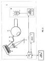
- Fig. 2 is a diagram illustrating a print media scanner 6 according to a preferred embodiment of the invention.
- the print media scanner includes a lamp 11 which produces light that is diffused in a integrating diffuser 21.
- the integrating diffuser then directs the light onto a print media 31 that is being scanned.
- the print media is moved relative to the scanning area, thereby allowing any length of print media to be scanned.
- the light that reflects off the print media then passes through a lens 41 which focuses the image on a light sensor 51.
- the light sensor is a grayscale or color CCD that is many pixels high and a few pixels wide. This allows the CCD to scan the entire height of the print media at once, but only a narrow width of the print media at a time.
- the entire width of the print media is scanned as the print media is moved relative to the light sensor.
- some of the light from the lamp is passed around the print media by optical fiber 61.
- the optical fiber is aimed so that the light is directed to pass through a lens 42 and is focused on sensor 51 in an area of the sensor not used for imaging the scanned print media.
- this rerouted light is from the same integrated mix of all the light coming from the lamp that illuminates the print media.
- the rerouted light is typically not bright, but is attenuated to match the light attenuated by the print media.
- optical fibers are utilized to reroute some of the light from the lamp, alternative embodiments may use other types of rerouting including mirror assemblies or the like.
- Light sensor 51 then provides pixel data signals to a DSP (Digital Signal Processor) 61.
- the DSP uses the pixel data signals to store data representing an image of the scanned print media in memory 71.
- the DSP may also communicate with a host computer 91 such as to provide image information to the host computer.
- the DSP may also control or send signals to a light assembly 86 if the light is determined to exceed predetermined ranges.
- Light assembly 86 includes a light control apparatus 81 and lamp 11.
- Light control apparatus 81 may include a power supply and other circuitry to vary the amount of light provided to lamp 11.
- ambient light may be used such that light apparatus 86 is not needed, such as in a hand scanner without an internal light source.
- the voltage scan from the CCD sensor is typically linear with respect to illumination.
- the variation in the lamp and sensor may be corrected. This will be described in greater detail below with respect to Fig. 4.
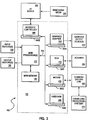
- Fig. 3 is a block diagram of a typical digital computer 100 that may be utilized by a preferred embodiment of the invention.
- the computer includes main processor(s) 110 coupled to a main memory 120 in computer box 105 with input device(s) 130 and output device(s) 140 attached.
- Main processor(s) 110 may include a single processor or multiple processors.
- Input device(s) 130 may include a keyboard, mouse, tablet or other types of input devices.
- Output device(s) 140 may include a text monitor, plotter or other types of output devices.
- the main processor may also be coupled to graphics output device(s) 210 such as a graphics display through a graphics adapter 200. Graphics adapter 200 may be located in an adapter slot 160A.
- Graphics adapter 200 receives instructions regarding graphics from main processor 110 on bus 150, thereby rendering the desired graphics output from the main processor.
- a scanner 206 may be coupled to a SCSI adapter 205 located in slot 160B. The scanner may be coupled to the host computer in other ways such as through a parallel or serial port.
- a modem or other communications adapter 250 and a hard disk 255 may also be located in slots 160C and 160D to provide communications with main processor 110 across bus 150. Modem 250 may communicate with other data processing systems 270 across communications line 260.
- Computer readable removable media 290 such as a magnetic diskette or a compact disc, may be inserted into an input/output device 285, such as a disk drive or a CD-ROM (compact disc - read only memory) driver.
- Data is read from or written to the removable media by the I/O device under the control of the I/O device controller 280.
- the I/O device controller communicates with the main processor through slot 160E across bus 150.
- Main memory 120, hard disk 255 and removable media 290 are all referred to as memory for storing data for processing by processor 110.
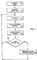
- Fig. 4 is a flowchart illustrating the operation of the film or print media scanners described above.
- a calibration scan is performed to determine an average brightness of the lamp and to determine a profile of the sensitivity of the various pixels on the light sensor.
- this calibration scan is preferably performed with no film in the device.
- the calibration is preferably performed without any media but with a reflective surface in its place.
- a profile table is generated by the DSP and stored in memory.
- this profile table includes a value for each pixel of the light sensor. The stored value is preferably the reciprocal of the average value determined by that pixel during the calibration scan.
- a multiplier is provided for the pixels that are directly illuminated by the light through the fiber optic cables.
- a set of multipliers are stored for use in subsequent scanning of objects (film, print media, etc.) as described below.
- step 340 the values from step 330 are multiplied by the corrective variation of light to correct any image variations caused by variations of the lamp illumination. This will eliminate any vertical lines caused by the lamp variations as the film or print media is moved horizontally through the scanner.
Landscapes
- Engineering & Computer Science (AREA)
- Multimedia (AREA)
- Signal Processing (AREA)
- Facsimile Scanning Arrangements (AREA)
- Facsimile Image Signal Circuits (AREA)
- Preparing Plates And Mask In Photomechanical Process (AREA)
- Image Input (AREA)
Applications Claiming Priority (2)
| Application Number | Priority Date | Filing Date | Title |
|---|---|---|---|
| US168700 | 1993-12-16 | ||
| US08/168,700 US5406070A (en) | 1993-12-16 | 1993-12-16 | Method and apparatus for scanning an object and correcting image data using concurrently generated illumination data |
Publications (2)
| Publication Number | Publication Date |
|---|---|
| EP0659013A2 true EP0659013A2 (fr) | 1995-06-21 |
| EP0659013A3 EP0659013A3 (fr) | 1995-10-25 |
Family
ID=22612584
Family Applications (1)
| Application Number | Title | Priority Date | Filing Date |
|---|---|---|---|
| EP94307335A Withdrawn EP0659013A3 (fr) | 1993-12-16 | 1994-10-06 | Procédé et dispositif pour balayer un objet. |
Country Status (4)
| Country | Link |
|---|---|
| US (1) | US5406070A (fr) |
| EP (1) | EP0659013A3 (fr) |
| JP (1) | JPH07236030A (fr) |
| KR (1) | KR950019810A (fr) |
Cited By (3)
| Publication number | Priority date | Publication date | Assignee | Title |
|---|---|---|---|---|
| EP1460839A4 (fr) * | 2001-12-21 | 2006-03-15 | Hamamatsu Photonics Kk | Dispositif d'imagerie |
| EP1455522A3 (fr) * | 2003-03-04 | 2006-09-20 | Thomson Licensing | Procédé de compensation des fluctuations d'une source de lumière et analyseur de film équipé de ce dispositif |
| GB2429865A (en) * | 2005-09-06 | 2007-03-07 | Cintel Internat Ltd | Optical scatter correction for film scanners |
Families Citing this family (37)
| Publication number | Priority date | Publication date | Assignee | Title |
|---|---|---|---|---|
| US5514864A (en) * | 1994-03-25 | 1996-05-07 | Umax Data System Inc. | Photo electric feedback compensation controlled apparatus |
| US6172705B1 (en) * | 1996-09-12 | 2001-01-09 | Pixar | Method and apparatus for a film scanner interface |
| US6400468B1 (en) * | 1998-03-31 | 2002-06-04 | International Business Machines Corporation | Smoothing calibration files to improve reproduction of digitized images |
| US6256111B1 (en) * | 1998-06-19 | 2001-07-03 | International Business Machines Corporation | Calibrating digital halftoning algorithms with multiple personalities |
| US6219140B1 (en) | 1998-12-16 | 2001-04-17 | Eastman Kodak Company | Apparatus for compensation for spectral fluctuation of a light source and a scanner incorporating said apparatus |
| US6462772B1 (en) | 1998-12-23 | 2002-10-08 | Eastman Kodak Company | Method of calibrating image scanning apparatus of a photographic film scanner |
| US7492488B2 (en) * | 2001-04-11 | 2009-02-17 | Cathy Liu | Image scanning system and method for scanner |
| US7251065B2 (en) * | 2002-01-31 | 2007-07-31 | Eastman Kodak Company | Image color balance for scanners using an illumination spectral sensor |
| US20080162219A1 (en) * | 2004-06-14 | 2008-07-03 | Symphonyrpm, Inc. | Decision object for associating a plurality of business plans |
| DE102004056722B4 (de) * | 2004-11-19 | 2006-09-28 | Deutsches Zentrum für Luft- und Raumfahrt e.V. | Filmscanner und ein Scanverfahren zum Unterdrücken von Helligkeitsschwankungen einer Strahlungsquelle |
| US7848561B2 (en) * | 2005-12-30 | 2010-12-07 | Honeywell International Inc. | Determining capability of an on-line sensor |
| US8478386B2 (en) | 2006-01-10 | 2013-07-02 | Accuvein Inc. | Practitioner-mounted micro vein enhancer |
| US11278240B2 (en) | 2006-01-10 | 2022-03-22 | Accuvein, Inc. | Trigger-actuated laser vein contrast enhancer |
| US10813588B2 (en) | 2006-01-10 | 2020-10-27 | Accuvein, Inc. | Micro vein enhancer |
| US9492117B2 (en) | 2006-01-10 | 2016-11-15 | Accuvein, Inc. | Practitioner-mounted micro vein enhancer |
| US8838210B2 (en) * | 2006-06-29 | 2014-09-16 | AccuView, Inc. | Scanned laser vein contrast enhancer using a single laser |
| US12295744B2 (en) | 2006-01-10 | 2025-05-13 | Accuvein, Inc. | Micro vein enhancer with two lasers and two optical detectors configured for removing surface topology |
| US9854977B2 (en) | 2006-01-10 | 2018-01-02 | Accuvein, Inc. | Scanned laser vein contrast enhancer using a single laser, and modulation circuitry |
| US12408865B2 (en) | 2006-01-10 | 2025-09-09 | Accuvein Inc. | Vein imaging device with differential image resolution at the center and the extremities of the vein image |
| US12089951B2 (en) | 2006-01-10 | 2024-09-17 | AccuVeiw, Inc. | Scanned laser vein contrast enhancer with scanning correlated to target distance |
| US8489178B2 (en) | 2006-06-29 | 2013-07-16 | Accuvein Inc. | Enhanced laser vein contrast enhancer with projection of analyzed vein data |
| US12471844B2 (en) | 2006-06-29 | 2025-11-18 | Accuvein, Inc. | Scanned laser vein contrast enhancer with full stopping of scanner movement during scan line reversals |
| US10238294B2 (en) | 2006-06-29 | 2019-03-26 | Accuvein, Inc. | Scanned laser vein contrast enhancer using one laser |
| US11253198B2 (en) | 2006-01-10 | 2022-02-22 | Accuvein, Inc. | Stand-mounted scanned laser vein contrast enhancer |
| US8255040B2 (en) * | 2006-06-29 | 2012-08-28 | Accuvein, Llc | Micro vein enhancer |
| US8244333B2 (en) * | 2006-06-29 | 2012-08-14 | Accuvein, Llc | Scanned laser vein contrast enhancer |
| US8594770B2 (en) * | 2006-06-29 | 2013-11-26 | Accuvein, Inc. | Multispectral detection and presentation of an object's characteristics |
| US8730321B2 (en) * | 2007-06-28 | 2014-05-20 | Accuvein, Inc. | Automatic alignment of a contrast enhancement system |
| US20160296146A9 (en) * | 2006-06-29 | 2016-10-13 | Fred Wood | Apparatus-Mounted Vein Contrast Enchancer |
| US8665507B2 (en) * | 2006-06-29 | 2014-03-04 | Accuvein, Inc. | Module mounting mirror endoscopy |
| US8463364B2 (en) * | 2009-07-22 | 2013-06-11 | Accuvein Inc. | Vein scanner |
| US9061109B2 (en) | 2009-07-22 | 2015-06-23 | Accuvein, Inc. | Vein scanner with user interface |
| CN103403531A (zh) | 2010-12-22 | 2013-11-20 | 皇家飞利浦电子股份有限公司 | 用于测试发光薄膜的方法和装置 |
| US9389188B2 (en) | 2010-12-22 | 2016-07-12 | Koninklijke Philips N.V. | Method and apparatus for testing optical films |
| US9072426B2 (en) | 2012-08-02 | 2015-07-07 | AccuVein, Inc | Device for detecting and illuminating vasculature using an FPGA |
| US10517483B2 (en) | 2012-12-05 | 2019-12-31 | Accuvein, Inc. | System for detecting fluorescence and projecting a representative image |
| US11924575B1 (en) * | 2023-03-30 | 2024-03-05 | Media Matters Llc | Conversion of color film to digital media |
Family Cites Families (24)
| Publication number | Priority date | Publication date | Assignee | Title |
|---|---|---|---|---|
| US307031A (en) * | 1884-10-21 | Thomas a | ||
| FR2440668A1 (fr) * | 1978-11-03 | 1980-05-30 | Thomson Csf | Dispositif d'analyse par photosenseur et appareil de fac-simile comportant un tel dispositif |
| JPS5995769A (ja) * | 1982-11-25 | 1984-06-01 | Hitachi Ltd | Ccdセンサ駆動装置 |
| US4639608A (en) * | 1983-05-18 | 1987-01-27 | Canon Kabushiki Kaisha | Image read-out apparatus with light source driving means |
| JPS61114647A (ja) * | 1984-11-09 | 1986-06-02 | Sharp Corp | 画像読取装置 |
| JPS61284164A (ja) * | 1985-06-10 | 1986-12-15 | Fuji Xerox Co Ltd | 照明用光源の駆動方法および装置 |
| US5084772A (en) * | 1986-10-31 | 1992-01-28 | Fuji Photo Film Co., Ltd. | Shading correcting method in image reading device |
| JP2595222B2 (ja) * | 1987-01-19 | 1997-04-02 | 工業技術院長 | 原稿読取装置 |
| JPS63180981A (ja) * | 1987-01-22 | 1988-07-26 | Nec Corp | 印刷装置 |
| EP0295491B1 (fr) * | 1987-06-04 | 1993-08-18 | Dainippon Screen Mfg. Co., Ltd. | Appareil et procédé pour stabiliser des quantités de lumière d'un lampe fluorescente |
| US4853739A (en) * | 1987-06-25 | 1989-08-01 | Minolta Camera Kabushiki Kaisha | Illuminating device for image exposure |
| US4961117A (en) * | 1987-11-13 | 1990-10-02 | New Dest Corporation | Document scanner |
| GB8801744D0 (en) * | 1988-01-27 | 1988-02-24 | Startronic Uk Ltd | Optical detection & control system |
| CA1287028C (fr) * | 1988-03-18 | 1991-07-30 | National Research Council Of Canada | Source lumineuse coaxiale repartie produisant un eclairement constant des cibles |
| US4868383A (en) * | 1988-09-08 | 1989-09-19 | Eastman Kodak Company | Linear integrating cavity light source used for generating an intense beam of light |
| JPH02116259A (ja) * | 1988-10-26 | 1990-04-27 | Toshiba Corp | 画像形成装置 |
| JP2751278B2 (ja) * | 1988-12-22 | 1998-05-18 | 富士ゼロックス株式会社 | 半導体レーザ走査装置 |
| JP2913660B2 (ja) * | 1989-04-07 | 1999-06-28 | ブラザー工業株式会社 | 画像読取装置 |
| US4998118A (en) * | 1989-07-03 | 1991-03-05 | Eastman Kodak Company | LED printhead with post lens optical feedback and method of controlling same |
| US5012346A (en) * | 1989-10-16 | 1991-04-30 | Eastman Kodak Company | Illumination system for a film scanner |
| EP0439358B1 (fr) * | 1990-01-25 | 1996-03-27 | Hewlett-Packard Company | Procédé et appareil pour la provision de compensation d'illumination dans un balayeur de documents |
| US5155596A (en) * | 1990-12-03 | 1992-10-13 | Eastman Kodak Company | Film scanner illumination system having an automatic light control |
| US5241459A (en) * | 1992-06-01 | 1993-08-31 | Eastman Kodak Company | Integrating cylinder with end input illumination for use as an illuminator in a film scanner |
| US5274228A (en) * | 1992-06-01 | 1993-12-28 | Eastman Kodak Company | Linear light source/collector with integrating cylinder and light pipe means |
-
1993
- 1993-12-16 US US08/168,700 patent/US5406070A/en not_active Expired - Lifetime
-
1994
- 1994-10-06 EP EP94307335A patent/EP0659013A3/fr not_active Withdrawn
- 1994-11-29 JP JP29433294A patent/JPH07236030A/ja active Pending
- 1994-12-07 KR KR1019940033145A patent/KR950019810A/ko not_active Abandoned
Cited By (6)
| Publication number | Priority date | Publication date | Assignee | Title |
|---|---|---|---|---|
| EP1460839A4 (fr) * | 2001-12-21 | 2006-03-15 | Hamamatsu Photonics Kk | Dispositif d'imagerie |
| US7245317B2 (en) | 2001-12-21 | 2007-07-17 | Hamamatsu Photonics K.K. | Imaging device having a luminous profile detecting element |
| EP1455522A3 (fr) * | 2003-03-04 | 2006-09-20 | Thomson Licensing | Procédé de compensation des fluctuations d'une source de lumière et analyseur de film équipé de ce dispositif |
| GB2429865A (en) * | 2005-09-06 | 2007-03-07 | Cintel Internat Ltd | Optical scatter correction for film scanners |
| GB2429865B (en) * | 2005-09-06 | 2011-02-23 | Cintel Internat Ltd | Optical scatter correction for film scanners |
| US8009190B2 (en) | 2005-09-06 | 2011-08-30 | Cintel International Limited | Optical scatter correction for film scanners |
Also Published As
| Publication number | Publication date |
|---|---|
| JPH07236030A (ja) | 1995-09-05 |
| EP0659013A3 (fr) | 1995-10-25 |
| US5406070A (en) | 1995-04-11 |
| KR950019810A (ko) | 1995-07-24 |
Similar Documents
| Publication | Publication Date | Title |
|---|---|---|
| US5406070A (en) | Method and apparatus for scanning an object and correcting image data using concurrently generated illumination data | |
| US6606171B1 (en) | Digitizing scanner | |
| US5278674A (en) | Method and apparatus for providing illumination compensation in a document scanner | |
| US5414535A (en) | Apparatus for reading image from original image on translucent film with automatic adjustment of the quantity of light from a light source | |
| US5206501A (en) | Image-reading device having a photoelectric transducer | |
| US4888492A (en) | Image reading apparatus | |
| EP0679010A2 (fr) | Appareil et procédé pour la lecture d'images, procédé de correction de niveau de blanc et procédé de génération de niveau de blanc | |
| US4639781A (en) | Dynamic gain adjuster for an image scanner | |
| JP3203018B2 (ja) | スキャナの照明性能の診断方法 | |
| US6862117B1 (en) | Method and apparatus for reducing the effect of bleed-through on captured images | |
| US5014332A (en) | Image reader | |
| JP3061423B2 (ja) | 文書スキャナ | |
| JP3098448B2 (ja) | 画像入力装置 | |
| JPH11168600A (ja) | 画像読み取り装置 | |
| US6204937B1 (en) | Image reading device with a built-in shielding device and related image scanning method | |
| JPH1198329A (ja) | 画像読取装置と画像読取方法 | |
| US6256117B1 (en) | Distinguishing method for object scanned by scanning device | |
| JP2936015B2 (ja) | 表面状態検査方法 | |
| US5157522A (en) | Method and apparatus for providing correction of hologon transmission efficiency variations | |
| EP2124429A1 (fr) | Scanner de documents | |
| US7463390B2 (en) | Information reading apparatus, method and system for processing image, program, and recording medium | |
| US6333498B1 (en) | Reduction of integrating cavity effect in scanners using polarizing filters | |
| JP3587109B2 (ja) | 画像入力装置 | |
| KR100331914B1 (ko) | 화상 입력 장치 및 방법 | |
| JP2001274941A (ja) | 画像読取システムの検査装置および検査方法 |
Legal Events
| Date | Code | Title | Description |
|---|---|---|---|
| PUAI | Public reference made under article 153(3) epc to a published international application that has entered the european phase |
Free format text: ORIGINAL CODE: 0009012 |
|
| AK | Designated contracting states |
Kind code of ref document: A2 Designated state(s): DE FR GB |
|
| PUAL | Search report despatched |
Free format text: ORIGINAL CODE: 0009013 |
|
| AK | Designated contracting states |
Kind code of ref document: A3 Designated state(s): DE FR GB |
|
| 17P | Request for examination filed |
Effective date: 19951024 |
|
| 17Q | First examination report despatched |
Effective date: 19971118 |
|
| STAA | Information on the status of an ep patent application or granted ep patent |
Free format text: STATUS: THE APPLICATION IS DEEMED TO BE WITHDRAWN |
|
| 18D | Application deemed to be withdrawn |
Effective date: 19980331 |