EP0660380A2 - Ajustage de la bande interdite d'une structure semi-conductrice à puits quantiques - Google Patents
Ajustage de la bande interdite d'une structure semi-conductrice à puits quantiques Download PDFInfo
- Publication number
- EP0660380A2 EP0660380A2 EP94309534A EP94309534A EP0660380A2 EP 0660380 A2 EP0660380 A2 EP 0660380A2 EP 94309534 A EP94309534 A EP 94309534A EP 94309534 A EP94309534 A EP 94309534A EP 0660380 A2 EP0660380 A2 EP 0660380A2
- Authority
- EP
- European Patent Office
- Prior art keywords
- quantum well
- well structure
- disordered region
- region
- disordered
- Prior art date
- Legal status (The legal status is an assumption and is not a legal conclusion. Google has not performed a legal analysis and makes no representation as to the accuracy of the status listed.)
- Granted
Links
Images


Classifications
-
- G—PHYSICS
- G02—OPTICS
- G02B—OPTICAL ELEMENTS, SYSTEMS OR APPARATUS
- G02B6/00—Light guides; Structural details of arrangements comprising light guides and other optical elements, e.g. couplings
- G02B6/10—Light guides; Structural details of arrangements comprising light guides and other optical elements, e.g. couplings of the optical waveguide type
- G02B6/12—Light guides; Structural details of arrangements comprising light guides and other optical elements, e.g. couplings of the optical waveguide type of the integrated circuit kind
- G02B6/13—Integrated optical circuits characterised by the manufacturing method
- G02B6/134—Integrated optical circuits characterised by the manufacturing method by substitution by dopant atoms
- G02B6/1347—Integrated optical circuits characterised by the manufacturing method by substitution by dopant atoms using ion implantation
-
- B—PERFORMING OPERATIONS; TRANSPORTING
- B82—NANOTECHNOLOGY
- B82Y—SPECIFIC USES OR APPLICATIONS OF NANOSTRUCTURES; MEASUREMENT OR ANALYSIS OF NANOSTRUCTURES; MANUFACTURE OR TREATMENT OF NANOSTRUCTURES
- B82Y20/00—Nanooptics, e.g. quantum optics or photonic crystals
-
- H—ELECTRICITY
- H10—SEMICONDUCTOR DEVICES; ELECTRIC SOLID-STATE DEVICES NOT OTHERWISE PROVIDED FOR
- H10P—GENERIC PROCESSES OR APPARATUS FOR THE MANUFACTURE OR TREATMENT OF DEVICES COVERED BY CLASS H10
- H10P14/00—Formation of materials, e.g. in the shape of layers or pillars
- H10P14/20—Formation of materials, e.g. in the shape of layers or pillars of semiconductor materials
- H10P14/32—Formation of materials, e.g. in the shape of layers or pillars of semiconductor materials characterised by intermediate layers between substrates and deposited layers
- H10P14/3202—Materials thereof
- H10P14/3214—Materials thereof being Group IIIA-VA semiconductors
- H10P14/3221—Arsenides
-
- H—ELECTRICITY
- H10—SEMICONDUCTOR DEVICES; ELECTRIC SOLID-STATE DEVICES NOT OTHERWISE PROVIDED FOR
- H10P—GENERIC PROCESSES OR APPARATUS FOR THE MANUFACTURE OR TREATMENT OF DEVICES COVERED BY CLASS H10
- H10P14/00—Formation of materials, e.g. in the shape of layers or pillars
- H10P14/20—Formation of materials, e.g. in the shape of layers or pillars of semiconductor materials
- H10P14/32—Formation of materials, e.g. in the shape of layers or pillars of semiconductor materials characterised by intermediate layers between substrates and deposited layers
- H10P14/3242—Structure
- H10P14/3244—Layer structure
- H10P14/3251—Layer structure consisting of three or more layers
- H10P14/3252—Alternating layers, e.g. superlattice
-
- H—ELECTRICITY
- H10—SEMICONDUCTOR DEVICES; ELECTRIC SOLID-STATE DEVICES NOT OTHERWISE PROVIDED FOR
- H10P—GENERIC PROCESSES OR APPARATUS FOR THE MANUFACTURE OR TREATMENT OF DEVICES COVERED BY CLASS H10
- H10P14/00—Formation of materials, e.g. in the shape of layers or pillars
- H10P14/20—Formation of materials, e.g. in the shape of layers or pillars of semiconductor materials
- H10P14/34—Deposited materials, e.g. layers
- H10P14/3402—Deposited materials, e.g. layers characterised by the chemical composition
- H10P14/3414—Deposited materials, e.g. layers characterised by the chemical composition being group IIIA-VIA materials
- H10P14/3421—Arsenides
-
- H—ELECTRICITY
- H10—SEMICONDUCTOR DEVICES; ELECTRIC SOLID-STATE DEVICES NOT OTHERWISE PROVIDED FOR
- H10P—GENERIC PROCESSES OR APPARATUS FOR THE MANUFACTURE OR TREATMENT OF DEVICES COVERED BY CLASS H10
- H10P14/00—Formation of materials, e.g. in the shape of layers or pillars
- H10P14/20—Formation of materials, e.g. in the shape of layers or pillars of semiconductor materials
- H10P14/38—Formation of materials, e.g. in the shape of layers or pillars of semiconductor materials characterised by treatments done after the formation of the materials
- H10P14/3822—Controlling the interface between substrate and epitaxial layer, e.g. by ion implantation followed by annealing
-
- H—ELECTRICITY
- H10—SEMICONDUCTOR DEVICES; ELECTRIC SOLID-STATE DEVICES NOT OTHERWISE PROVIDED FOR
- H10P—GENERIC PROCESSES OR APPARATUS FOR THE MANUFACTURE OR TREATMENT OF DEVICES COVERED BY CLASS H10
- H10P14/00—Formation of materials, e.g. in the shape of layers or pillars
- H10P14/20—Formation of materials, e.g. in the shape of layers or pillars of semiconductor materials
- H10P14/38—Formation of materials, e.g. in the shape of layers or pillars of semiconductor materials characterised by treatments done after the formation of the materials
- H10P14/3824—Intermixing, interdiffusion or disordering of III-V heterostructures, e.g. IILD
-
- G—PHYSICS
- G02—OPTICS
- G02B—OPTICAL ELEMENTS, SYSTEMS OR APPARATUS
- G02B6/00—Light guides; Structural details of arrangements comprising light guides and other optical elements, e.g. couplings
- G02B6/10—Light guides; Structural details of arrangements comprising light guides and other optical elements, e.g. couplings of the optical waveguide type
- G02B6/12—Light guides; Structural details of arrangements comprising light guides and other optical elements, e.g. couplings of the optical waveguide type of the integrated circuit kind
- G02B2006/12166—Manufacturing methods
- G02B2006/12169—Annealing
-
- H—ELECTRICITY
- H01—ELECTRIC ELEMENTS
- H01S—DEVICES USING THE PROCESS OF LIGHT AMPLIFICATION BY STIMULATED EMISSION OF RADIATION [LASER] TO AMPLIFY OR GENERATE LIGHT; DEVICES USING STIMULATED EMISSION OF ELECTROMAGNETIC RADIATION IN WAVE RANGES OTHER THAN OPTICAL
- H01S5/00—Semiconductor lasers
- H01S5/30—Structure or shape of the active region; Materials used for the active region
- H01S5/34—Structure or shape of the active region; Materials used for the active region comprising quantum well or superlattice structures, e.g. single quantum well [SQW] lasers, multiple quantum well [MQW] lasers or graded index separate confinement heterostructure [GRINSCH] lasers
- H01S5/3413—Structure or shape of the active region; Materials used for the active region comprising quantum well or superlattice structures, e.g. single quantum well [SQW] lasers, multiple quantum well [MQW] lasers or graded index separate confinement heterostructure [GRINSCH] lasers comprising partially disordered wells or barriers
-
- H—ELECTRICITY
- H01—ELECTRIC ELEMENTS
- H01S—DEVICES USING THE PROCESS OF LIGHT AMPLIFICATION BY STIMULATED EMISSION OF RADIATION [LASER] TO AMPLIFY OR GENERATE LIGHT; DEVICES USING STIMULATED EMISSION OF ELECTROMAGNETIC RADIATION IN WAVE RANGES OTHER THAN OPTICAL
- H01S5/00—Semiconductor lasers
- H01S5/30—Structure or shape of the active region; Materials used for the active region
- H01S5/34—Structure or shape of the active region; Materials used for the active region comprising quantum well or superlattice structures, e.g. single quantum well [SQW] lasers, multiple quantum well [MQW] lasers or graded index separate confinement heterostructure [GRINSCH] lasers
- H01S5/3413—Structure or shape of the active region; Materials used for the active region comprising quantum well or superlattice structures, e.g. single quantum well [SQW] lasers, multiple quantum well [MQW] lasers or graded index separate confinement heterostructure [GRINSCH] lasers comprising partially disordered wells or barriers
- H01S5/3414—Structure or shape of the active region; Materials used for the active region comprising quantum well or superlattice structures, e.g. single quantum well [SQW] lasers, multiple quantum well [MQW] lasers or graded index separate confinement heterostructure [GRINSCH] lasers comprising partially disordered wells or barriers by vacancy induced interdiffusion
Definitions
- This invention relates to semiconductor heterostructures and, more specifically, to a method of selectively tuning the bandedge of a semiconductor heterostructure.
- Optical and electrical properties of quantum well structures are of great importance for novel semiconductor device applications.
- An ultimate goal of monolithic integration of optical, optoelectronic and electronic components requires the capability for controllable lateral and vertical modifications of optical constants and electrical characteristics in such components.
- Impurity induced compositional disordering is a well known technique for enhancing interdiffusion. It has been successfully applied to the fabrication of superlattice and quantum well heterostructure devices. In particular, IICD has been demonstrated in a variety of structures by using a diffusion process, and also by using ion implantation followed by thermal annealing. Experimental results have shown that ion implantation is a suitable technique for introducing many kinds of impurities into quantum well structures to enhance interdiffusion.
- the range profile of relevance to intermixing is always considered to be the range for energy losses to nuclear damage processes, and the enhancement of interdiffusion is always associated with the presence of implantation induced defects and/or impurities.
- the mass and energy of the implanted ions are always chosen such that the impurities/damage distribution are spatially peaked in the region of interest for intermixing, such as the middle of a multiple quantum well or a superlattice structure.
- Holonyak in U.S. Pat. No. 4,511,408 discloses a method for disordering the layers in a III-V heterostructure by implanting ions directly into the sample (region of intermixing) and then subjecting the sample to the thermal annealing. As noted in column 4, lines 30-34 the implantation causes considerable crystal damage in the structure, that in this case was a superlattice.
- the above method for enhancing interdiffusion at heterointerfaces is also disclosed by Hirayama et al. in "Ion-Species Dependence of Interdiffusion in Ion-Implanted GeAs-AlAs Superlattices", Japanese Journal of Applied Physics, 24, pp. 1498-15023 (1985), and by Cibert et al. in "Kinetics of Implantation Enhanced Interdiffusion of Ga and Al at GaAs-Ga x Al 1-x As Interfaces", Applied Physics Letters, 49(4), pp. 223-225(1986).
- Hirayama et al. implanted a group of samples containing superlattices with a variety of ion species and then measured the photoluminescence peak shifts while the samples were being annealed. As in Holonyak, the ions were implanted directly into the superlattice structure, causing crystal damage in the region of intermixing that required thermal treatment to effect recovery.
- Hirayama et al. observed that the spectral width of the superlattice structure increased after annealing, and explained that the increase is partly due to the inhomogeneity of the interdiffusion resulting from the inhomogenous depth profile of implanted impurity density. Cibert et al.
- Elman et al. in U.S. Patent No. 5,238,868 describe a method of selectively tuning the bandedge in a quantum well heterostructure.
- the method steps include implanting ions into the heterostructure to form a disordered region near the upper surface of the sample. Vacancies and defects created by the implantation step are spatially separated from the quantum well active region.
- the heterostructure is then thermally annealed so that the vacancies diffuse through the active region (quantum wells) and enhance interdiffusion at the heterojunctions thereby modifying the optical bandgap of the quantum well layers.
- This bandgap tuning is somewhat selective because the implantation step can be to an extent controlled.
- a method is provided of processing a semiconductor heterostructure having a single quantum well structure as an active region, wherein a cladding layer is deposited on said single quantum well structure, comprising the steps of:
- a method for processing a semiconductor heterostructure having a multiple quantum well structure as an active region, wherein a cladding layer is deposited on said multiple quantum well structure comprising the steps of:
- step (a) and (b) sequentially and repeatedly allows the bandgap to be further and further increased.
- This is somewhat surprising, as tests have shown that increasing the amount of implantation and increasing the anneal time without repeating steps (a) and (b) in the manner described by Elman et al. provides only a limited increase in the bandgap. In fact, after steadily increasing the amount of implantation or the duration of annealing, there is a peak point after which the bandgap actually begins to decrease.
- the method of this invention therefore, provides a process that is viable for the manufacture of semiconductor devices.
- the present application discloses a novel method for bandedge tuning in III-V semiconductor material systems by controlling the level of atomic interdiffusion at heterointerfaces of the system.
- the material systems of interest are semiconductor heterostructures having a quantum well structure as an active or part of an active region, and include such devices as a laser, detector, amplifier, modulator waveguide, etc.
- a heterostructure to be tuned is first implanted with low energy ions and then subjected to thermal annealing.
- implantation need not be limited to low energy ions.
- This process of implanting and annealing is subsequently repeated at least once and perhaps a number of times depending on the level of tuning required.
- Each implantation creates a disordered region near the upper surface of the heterostructure wherein the vacancies and defects are spatially separated from the quantum well region, thus ensuring that no damage will occur to the active region.
- the heterostructure is thermally annealed so that the vacancies diffuse into the quantum well structure and enhance the intermixing between atoms at the heterointerfaces.
- FIGS. 1A-1D were grown by molecular beam epitaxy in a RIBER 2300 system, and include a quantum well active region with alternating layers of a GaAs quantum well layer and an AlGaAs barrier layer. It should be well known to those skilled in the art that other quantum well structures having different compounds would be capable of being tuned in accordance with the present invention. Ion beam implantation was performed using 35 keV 75As+ ions having a fluence range of between 5 ⁇ 1013 cm ⁇ 2 and 5 ⁇ 1013 cm ⁇ 2. The samples were masked prior to implantation so that only half of each piece was implanted, allowing a direct comparison between the respective bandgap changes in the implanted and unimplanted areas.
- RTA rapid thermal annealing
- PL photoluminescence
- the heterostructures in FIGS. 1A and 1B consist of a quantum well active region 12 having a series of single quantum well layers labeled SQW1-SQW5 grown in standard and reverse order, respectively.
- the well layers are uncoupled and varying widths, with the layer SQW1 in each active region being located approximately 300 nm below the upper surface 10.
- a barrier layer separates adjacent quantum well layer SQW1, thereby preventing the defects created by ion implantation from damaging the active region 12. Consequently, the material quality of the well layers is preserved.
- thermal annealing is performed to enhance the interdiffusion at the well-barrier heterojunctions.
- FIG. 1C is a simple double heterostructure waveguide 13 with a 4 nm-wide control single quantum well layer 16 in the middle of 1.2 ⁇ m of GaAs.
- FIG. 1D shows a multiple quantum well waveguide 17 consisting of twenty-five periods of 8 nm GaAs single quantum well layers 18 separated by 8 nm of Al 0.3 Ga 0.7 As barriers 19.
- the upper surface 10 in each of FIGS. 1C and 1D was ion implanted to create a disordered region 11 of depth R p .
- the disordered region 11 in both FIGS. 1C and 1D is spatially separated from its respective region.
- FIGS. 1A-1D are for illustrative purposes only, and should not serve to limit the application of the novel tuning method to only these heterostructure devices. It should be apparent to those skilled in the art that other heterostructures containing quantum wells in the active region could be similarly tuned.
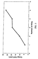
- An important aspect of the novel tuning method is that as the ion implantation and thermal annealing steps are sequentially repeated; a designer may therefore increase the bandedge of the device under investigation far beyond limits possible with a single implantation followed by rapid thermal annealing. This will be described particularly with reference to FIG 3.
- FIG. 2 it can be seen that as the focused ion beam (FIB) ion dose is increased, the (emission) energy shift which is proportional to the bandgap energy, increases montonically from approximately 0.5 meV to approximately 4 meV until it saturates. Unfortunately, further increasing the ion implantation dose beyond a fluence of about 1013 cm ⁇ 2 degrades the process so that the energy shift begins to decrease. This behaviour is a consequence of the fact that single, isolated vacancies have higher mobilities than the vacancy complexes that occur with greater probability when high fluences are employed. These complexes that are created tend to not move as readily when heat is applied.
- FIB focused ion beam
- FIG. 3 a large increase in bandgap shift is shown by using the method in accordance with this invention.
- the initial maximum 4 meV shift of FIG. 2 is increased to 11 meV after a second FIB implant and RTA. This is further increased to approximately 20 meV after a third implant and RTA.
- the fourth RTA which produced no further increase in bandgap shift was performed with no additional implant in order to verify that both implanting and RTA are necessary to effect additional bandgap shifts. Therefore the application of heat alone is not enough to create additional shift in the bandgap.
- the fifth RTA which produced an additional 8 meV shift was performed after another implant.
- the present invention can also be used to tune a group of quantum well regions in a spatially selective manner.
- the spatial selection is effected by masking a heterostructure in accordance with a specified pattern so that the unmasked portions correspond to designated regions of the structure where tuning is desirable.
- disordered regions are only formed in the unmasked areas.
- the vacancies and defects in each disordered region are spatially separated from their respective quantum well regions.
- Thermal treatment of the heterostructure causes enhanced interdiffusion to occur in only the quantum well regions of the unmasked areas.
- masking can be performed in combination with subsequent implanting followed by RTA to one or more regions of the heterostructure, thereby allowing for tuning within a very large bandgap range.
- other masks can be applied after the first masking and annealing and the process can be repeated. Fine tuning can be obtained by varying the parameters at each ion implant stage, and a broad range of tuning can be obtained by repeatedly implanting and annealing any particular region.
Landscapes
- Engineering & Computer Science (AREA)
- Physics & Mathematics (AREA)
- Optics & Photonics (AREA)
- Chemical & Material Sciences (AREA)
- Nanotechnology (AREA)
- Microelectronics & Electronic Packaging (AREA)
- General Physics & Mathematics (AREA)
- Life Sciences & Earth Sciences (AREA)
- Biophysics (AREA)
- Crystallography & Structural Chemistry (AREA)
- Semiconductor Lasers (AREA)
- Recrystallisation Techniques (AREA)
Applications Claiming Priority (2)
| Application Number | Priority Date | Filing Date | Title |
|---|---|---|---|
| US08/172,094 US5395793A (en) | 1993-12-23 | 1993-12-23 | Method of bandgap tuning of semiconductor quantum well structures |
| US172094 | 1993-12-23 |
Publications (3)
| Publication Number | Publication Date |
|---|---|
| EP0660380A2 true EP0660380A2 (fr) | 1995-06-28 |
| EP0660380A3 EP0660380A3 (fr) | 1996-01-03 |
| EP0660380B1 EP0660380B1 (fr) | 1999-06-09 |
Family
ID=22626336
Family Applications (1)
| Application Number | Title | Priority Date | Filing Date |
|---|---|---|---|
| EP94309534A Expired - Lifetime EP0660380B1 (fr) | 1993-12-23 | 1994-12-20 | Ajustage de la bande interdite d'une structure semi-conductrice à puits quantiques |
Country Status (4)
| Country | Link |
|---|---|
| US (1) | US5395793A (fr) |
| EP (1) | EP0660380B1 (fr) |
| CA (1) | CA2140619C (fr) |
| DE (1) | DE69418986T2 (fr) |
Cited By (3)
| Publication number | Priority date | Publication date | Assignee | Title |
|---|---|---|---|---|
| EP0852417A3 (fr) * | 1997-01-07 | 1998-09-23 | Sumitomo Electric Industries, Ltd. | Laser à semi-conducteur et méthode de sa production |
| US6719884B2 (en) | 2001-09-13 | 2004-04-13 | Intense Photonics Limited | Method of manufacturing optical devices and related improvements |
| US6760355B2 (en) | 2000-07-27 | 2004-07-06 | The University Court Of The University Of Glasgow | Semiconductor laser |
Families Citing this family (29)
| Publication number | Priority date | Publication date | Assignee | Title |
|---|---|---|---|---|
| US5766981A (en) * | 1995-01-04 | 1998-06-16 | Xerox Corporation | Thermally processed, phosphorus- or arsenic-containing semiconductor laser with selective IILD |
| US5757023A (en) * | 1996-01-25 | 1998-05-26 | National Research Council Of Canada | Fabrication of quantum well polarization independent active devices |
| DE19604348C2 (de) * | 1996-02-07 | 2003-10-23 | Deutsche Telekom Ag | Verfahren zur Herstellung einer kalibrierten Längenskala im Nanometerbereich für technische Geräte, die der hochauflösenden bis ultrahochauflösenden Abbildung von Strukturen dienen |
| US5815628A (en) * | 1996-04-17 | 1998-09-29 | Nec Corporation | Ordered semiconductor having periodical disorder and devices made therefrom |
| SG85604A1 (en) * | 1998-11-06 | 2002-01-15 | Inst Materials Research & Eng | Method of selective post-growth tuning of an optical bandgap of a semi-conductor heterostructure and products produced thereof |
| GB2351390A (en) | 1999-06-16 | 2000-12-27 | Sharp Kk | A semiconductor material comprising two dopants |
| WO2001088993A2 (fr) | 2000-05-19 | 2001-11-22 | Mcmaster University | Procede permettant de modifier localement l'energie efficace de bande interdite dans les structures de puits quantiques a indium gallium arsenure phosphure (ingaasp) |
| US6797533B2 (en) * | 2000-05-19 | 2004-09-28 | Mcmaster University | Quantum well intermixing in InGaAsP structures induced by low temperature grown InP |
| AUPR043900A0 (en) * | 2000-09-28 | 2000-10-26 | Australian National University, The | Method of disordering quantum well heterostructures by high energy ion irradiation |
| US6878562B2 (en) | 2000-10-20 | 2005-04-12 | Phosistor Technologies, Incorporated | Method for shifting the bandgap energy of a quantum well layer |
| FR2818390B1 (fr) * | 2000-12-15 | 2003-11-07 | Ion Beam Services | Guide d'onde comportant un canal sur un substrat optique |
| US6984538B2 (en) * | 2001-07-26 | 2006-01-10 | Phosistor Technologies, Inc. | Method for quantum well intermixing using pre-annealing enhanced defects diffusion |
| US6628686B1 (en) | 2001-11-16 | 2003-09-30 | Fox-Tek, Inc | Integrated multi-wavelength and wideband lasers |
| US6594295B1 (en) | 2001-11-16 | 2003-07-15 | Fox-Tek, Inc. | Semiconductor laser with disordered and non-disordered quantum well regions |
| US6731850B1 (en) | 2001-11-16 | 2004-05-04 | Fox-Tek | Single-waveguide integrated wavelength demux photodetector and method of making it |
| US6888666B1 (en) | 2001-11-16 | 2005-05-03 | Dakota Investment Group, Inc. | Dynamically reconfigurable optical amplification element |
| SG99970A1 (en) * | 2002-04-05 | 2003-11-27 | Inst Materials Research & Eng | Method for forming a modified semiconductor having a plurality of band gaps |
| US7035305B2 (en) * | 2002-05-10 | 2006-04-25 | Bookham Technology, Plc | Monolithically integrated high power laser optical device |
| FR2840689B1 (fr) * | 2002-06-06 | 2004-10-15 | Silios Technologies | Guide d'onde comportant un canal et une couche d'adaptation |
| GB2409333B (en) * | 2003-12-10 | 2006-07-26 | Intense Photonics Ltd | Multiple anneal induced disordering |
| GB2409572B (en) * | 2003-12-24 | 2006-02-15 | Intense Photonics Ltd | Generating multiple bandgaps using multiple epitaxial layers |
| US7804864B2 (en) | 2004-03-31 | 2010-09-28 | Imra America, Inc. | High power short pulse fiber laser |
| CA2632098A1 (fr) * | 2005-12-02 | 2007-06-07 | Helianthos B.V. | Pile photovoltaique |
| EP1883140B1 (fr) * | 2006-07-27 | 2013-02-27 | OSRAM Opto Semiconductors GmbH | LD ou DEL avec une couche de revêtment superréseau et dopage gradué |
| EP1883141B1 (fr) * | 2006-07-27 | 2017-05-24 | OSRAM Opto Semiconductors GmbH | LD ou DEL avec une couche de revêtement superréseau |
| EP1883119B1 (fr) * | 2006-07-27 | 2015-11-04 | OSRAM Opto Semiconductors GmbH | Structure de recouvrement semi-conductrice dotée d'une surgrille |
| DE102006046228A1 (de) * | 2006-07-27 | 2008-01-31 | Osram Opto Semiconductors Gmbh | Halbleiter-Schichtstruktur mit Übergitter |
| JP2009105184A (ja) * | 2007-10-23 | 2009-05-14 | Sharp Corp | 窒化物系半導体レーザ素子とその製造方法 |
| US8213751B1 (en) * | 2008-11-26 | 2012-07-03 | Optonet Inc. | Electronic-integration compatible photonic integrated circuit and method for fabricating electronic-integration compatible photonic integrated circuit |
Family Cites Families (5)
| Publication number | Priority date | Publication date | Assignee | Title |
|---|---|---|---|---|
| US4511408A (en) * | 1982-04-22 | 1985-04-16 | The Board Of Trustees Of The University Of Illinois | Semiconductor device fabrication with disordering elements introduced into active region |
| US4871690A (en) * | 1986-01-21 | 1989-10-03 | Xerox Corporation | Semiconductor structures utilizing semiconductor support means selectively pretreated with migratory defects |
| US4771010A (en) * | 1986-11-21 | 1988-09-13 | Xerox Corporation | Energy beam induced layer disordering (EBILD) |
| EP0429979A3 (en) * | 1989-11-30 | 1992-01-29 | Gte Laboratories Incorporated | Bandgap tuning of semiconductor quantum well structures |
| US5238868A (en) * | 1989-11-30 | 1993-08-24 | Gte Laboratories Incorporated | Bandgap tuning of semiconductor quantum well structures |
-
1993
- 1993-12-23 US US08/172,094 patent/US5395793A/en not_active Expired - Lifetime
-
1994
- 1994-12-12 CA CA002140619A patent/CA2140619C/fr not_active Expired - Fee Related
- 1994-12-20 EP EP94309534A patent/EP0660380B1/fr not_active Expired - Lifetime
- 1994-12-20 DE DE69418986T patent/DE69418986T2/de not_active Expired - Fee Related
Cited By (4)
| Publication number | Priority date | Publication date | Assignee | Title |
|---|---|---|---|---|
| EP0852417A3 (fr) * | 1997-01-07 | 1998-09-23 | Sumitomo Electric Industries, Ltd. | Laser à semi-conducteur et méthode de sa production |
| US6005881A (en) * | 1997-01-07 | 1999-12-21 | Sumitomo Electric Industries, Ltd. | Semiconductor laser and method of making the same |
| US6760355B2 (en) | 2000-07-27 | 2004-07-06 | The University Court Of The University Of Glasgow | Semiconductor laser |
| US6719884B2 (en) | 2001-09-13 | 2004-04-13 | Intense Photonics Limited | Method of manufacturing optical devices and related improvements |
Also Published As
| Publication number | Publication date |
|---|---|
| CA2140619A1 (fr) | 1995-06-24 |
| EP0660380B1 (fr) | 1999-06-09 |
| DE69418986D1 (de) | 1999-07-15 |
| EP0660380A3 (fr) | 1996-01-03 |
| US5395793A (en) | 1995-03-07 |
| CA2140619C (fr) | 2004-05-04 |
| DE69418986T2 (de) | 1999-09-30 |
Similar Documents
| Publication | Publication Date | Title |
|---|---|---|
| US5395793A (en) | Method of bandgap tuning of semiconductor quantum well structures | |
| US5238868A (en) | Bandgap tuning of semiconductor quantum well structures | |
| Charbonneau et al. | Quantum‐well intermixing for optoelectronic integration using high energy ion implantation | |
| US6984538B2 (en) | Method for quantum well intermixing using pre-annealing enhanced defects diffusion | |
| US20020072142A1 (en) | Method for shifting the bandgap energy of a quantum well layer | |
| Charbonneau et al. | Band‐gap tuning of InGaAs/InGaAsP/InP laser using high energy ion implantation | |
| Koteles et al. | Quantum well shape modification using vacancy generation and rapid thermal annealing | |
| Tan et al. | Wavelength shifting in GaAs quantum well lasers by proton irradiation | |
| Haysom et al. | Study of quantum well intermixing caused by grown-in defects | |
| Poole et al. | Demonstration of an ion-implanted, wavelength-shifted quantum-well laser | |
| Noël et al. | High‐reliability blue‐shifted InGaAsP/InP lasers | |
| Poole et al. | The enhancement of quantum well intermixing through repeated ion implantation | |
| EP0429979A2 (fr) | Ajustage de la bande interdite d'une structure semi-conductrice à puits quantiques | |
| Haysom et al. | Lateral selectivity of ion-induced quantum well intermixing | |
| US6936526B2 (en) | Method of disordering quantum well heterostructures | |
| Cao et al. | Band-gap blue shift by impurity-free vacancy diffusion in 1.5-μm-strained InGaAsP/InP multiple quantum-well laser structure | |
| Charbonneau et al. | Bandgap tuning of semiconductor Quantum Well laser structures using high energy ion implantation | |
| US20070160099A1 (en) | Multiple anneal induced disordering | |
| Younis et al. | Characterization and optimization of ion implantation for high spatial resolution quantum well intermixing in GaAs/AlGaAs superlattices | |
| Goldberg et al. | Ion beam intermixing of semiconductor heterostructures for optoelectronic applications | |
| Xiong et al. | MeV ion beam processing of III–V compound semiconductors | |
| Piva et al. | Bandgap tuning of semiconductor quantum well structures using ion implantation | |
| Goldberg et al. | Selective intermixing of ion irradiated semiconductor heterostructures | |
| Kalish et al. | Ion implantation into quantum-well structures | |
| Gillin et al. | The effect of gallium implantation on the intermixing of InGaAs/GaAs strained quantum wells |
Legal Events
| Date | Code | Title | Description |
|---|---|---|---|
| PUAI | Public reference made under article 153(3) epc to a published international application that has entered the european phase |
Free format text: ORIGINAL CODE: 0009012 |
|
| AK | Designated contracting states |
Kind code of ref document: A2 Designated state(s): DE FR GB IT |
|
| PUAL | Search report despatched |
Free format text: ORIGINAL CODE: 0009013 |
|
| AK | Designated contracting states |
Kind code of ref document: A3 Designated state(s): DE FR GB IT |
|
| K1C1 | Correction of patent application (title page) published |
Effective date: 19950628 |
|
| 17P | Request for examination filed |
Effective date: 19960426 |
|
| 17Q | First examination report despatched |
Effective date: 19971024 |
|
| GRAG | Despatch of communication of intention to grant |
Free format text: ORIGINAL CODE: EPIDOS AGRA |
|
| GRAG | Despatch of communication of intention to grant |
Free format text: ORIGINAL CODE: EPIDOS AGRA |
|
| GRAH | Despatch of communication of intention to grant a patent |
Free format text: ORIGINAL CODE: EPIDOS IGRA |
|
| GRAH | Despatch of communication of intention to grant a patent |
Free format text: ORIGINAL CODE: EPIDOS IGRA |
|
| GRAA | (expected) grant |
Free format text: ORIGINAL CODE: 0009210 |
|
| AK | Designated contracting states |
Kind code of ref document: B1 Designated state(s): DE FR GB IT |
|
| PG25 | Lapsed in a contracting state [announced via postgrant information from national office to epo] |
Ref country code: IT Free format text: LAPSE BECAUSE OF FAILURE TO SUBMIT A TRANSLATION OF THE DESCRIPTION OR TO PAY THE FEE WITHIN THE PRE;WARNING: LAPSES OF ITALIAN PATENTS WITH EFFECTIVE DATE BEFORE 2007 MAY HAVE OCCURRED AT ANY TIME BEFORE 2007. THE CORRECT EFFECTIVE DATE MAY BE DIFFERENT FROM THE ONE RECORDED.SCRIBED TIME-LIMIT Effective date: 19990609 Ref country code: FR Free format text: LAPSE BECAUSE OF FAILURE TO SUBMIT A TRANSLATION OF THE DESCRIPTION OR TO PAY THE FEE WITHIN THE PRESCRIBED TIME-LIMIT Effective date: 19990609 |
|
| REF | Corresponds to: |
Ref document number: 69418986 Country of ref document: DE Date of ref document: 19990715 |
|
| EN | Fr: translation not filed | ||
| PLBE | No opposition filed within time limit |
Free format text: ORIGINAL CODE: 0009261 |
|
| STAA | Information on the status of an ep patent application or granted ep patent |
Free format text: STATUS: NO OPPOSITION FILED WITHIN TIME LIMIT |
|
| 26N | No opposition filed | ||
| REG | Reference to a national code |
Ref country code: GB Ref legal event code: IF02 |
|
| PGFP | Annual fee paid to national office [announced via postgrant information from national office to epo] |
Ref country code: GB Payment date: 20031217 Year of fee payment: 10 |
|
| PGFP | Annual fee paid to national office [announced via postgrant information from national office to epo] |
Ref country code: DE Payment date: 20040102 Year of fee payment: 10 |
|
| PG25 | Lapsed in a contracting state [announced via postgrant information from national office to epo] |
Ref country code: GB Free format text: LAPSE BECAUSE OF NON-PAYMENT OF DUE FEES Effective date: 20041220 |
|
| PG25 | Lapsed in a contracting state [announced via postgrant information from national office to epo] |
Ref country code: DE Free format text: LAPSE BECAUSE OF NON-PAYMENT OF DUE FEES Effective date: 20050701 |
|
| GBPC | Gb: european patent ceased through non-payment of renewal fee |
Effective date: 20041220 |