EP0660385B1 - Intelligente Prüfungsstrasse - Google Patents
Intelligente Prüfungsstrasse Download PDFInfo
- Publication number
- EP0660385B1 EP0660385B1 EP94119756A EP94119756A EP0660385B1 EP 0660385 B1 EP0660385 B1 EP 0660385B1 EP 94119756 A EP94119756 A EP 94119756A EP 94119756 A EP94119756 A EP 94119756A EP 0660385 B1 EP0660385 B1 EP 0660385B1
- Authority
- EP
- European Patent Office
- Prior art keywords
- burn
- quality
- information
- test
- wafer
- Prior art date
- Legal status (The legal status is an assumption and is not a legal conclusion. Google has not performed a legal analysis and makes no representation as to the accuracy of the status listed.)
- Expired - Lifetime
Links
Images

Classifications
-
- G—PHYSICS
- G01—MEASURING; TESTING
- G01R—MEASURING ELECTRIC VARIABLES; MEASURING MAGNETIC VARIABLES
- G01R31/00—Arrangements for testing electric properties; Arrangements for locating electric faults; Arrangements for electrical testing characterised by what is being tested not provided for elsewhere
- G01R31/26—Testing of individual semiconductor devices
-
- H—ELECTRICITY
- H10—SEMICONDUCTOR DEVICES; ELECTRIC SOLID-STATE DEVICES NOT OTHERWISE PROVIDED FOR
- H10P—GENERIC PROCESSES OR APPARATUS FOR THE MANUFACTURE OR TREATMENT OF DEVICES COVERED BY CLASS H10
- H10P74/00—Testing or measuring during manufacture or treatment of wafers, substrates or devices
- H10P74/23—Testing or measuring during manufacture or treatment of wafers, substrates or devices characterised by multiple measurements, corrections, marking or sorting processes
-
- H—ELECTRICITY
- H10—SEMICONDUCTOR DEVICES; ELECTRIC SOLID-STATE DEVICES NOT OTHERWISE PROVIDED FOR
- H10P—GENERIC PROCESSES OR APPARATUS FOR THE MANUFACTURE OR TREATMENT OF DEVICES COVERED BY CLASS H10
- H10P74/00—Testing or measuring during manufacture or treatment of wafers, substrates or devices
Definitions
- the present invention relates to a system and method for efficiently testing ICs (integrated circuits).
- a burn-in test condition is determined from the viewpoint of ensuring the reliability of ICs for a predetermined period of time. This condition remains the same for both poor-quality ICs which are susceptible to failure and high-quality ICs which are less susceptible to failure.
- the predicted failure rate is a ratio of defective IC chips predicted to be produced within a predetermined period of time to a plurality of IC chips on one base member (e.g., a wafer) on which a screen test has been conducted.
- This predicted failure rate is determined to be a minimum constant value.
- a test system including an existing burn-in test is designed such that even the failure rate of poorest-quality products do not exceed a predicted failure rate.
- US-A-4 985 988 describes an assembly flow in which integrated circuits are burned-in and parametrically tested before assembly is provided.
- the integrated circuits are sorted based on the results of the parametric testing, and assembled in groups with similar parameters.
- Integrated circuits from a single group are assembled on a leadframe and encapsulated, marked, and tested again while still attached to the leadframe.
- the packaged integrated circuits are separated from the leadframe and those meeting predetermined parameters are loaded into carrier sleeves.
- a screening test The purpose of a screening test is to remove defective products, but the test itself produces no value to be added. Therefore, the cost for a screening test must be minimized.
- test time increases by 10 times for each new generation (with an increase in degree of integration). That is, the test time for a 4-Mbyte DRAM is 10 times that for a 1-Mbyte DRAM. Therefore, in order to ensure the same production of 4-Mbyte DRAMs as that of 1-Mbyte DRAMS, the production facilities for 4-Mbytes DRAMs need to be 10 times as large as those for 1-Mbyte DRAMS.
- the screening test cost of 4-Mbyte DRAMs is 10 times or more that of 1-Mbyte DRAMS.
- the memory size of a 4-Mbyte DRAM is four times that of a 1-Mbyte DRAM. It is, therefore, required that the cost of 4-Mbyte DRAMs be four times or less that of 1-Mbyte DRAMs.
- the present invention has been made to eliminate the above drawbacks, and has as its object to reduce the test cost without increasing the test time even if ICs decrease in size and increase in capacity.
- a method of manufacturing integrated circuits comprising the following steps in the given order: processing a plurality of wafers to form IC chips thereon and collecting primary information concerning the quality of the process to which each wafer was subjected; evaluating the plurality of IC chips on each wafer to obtain secondary information concerning the quality of each chip; determining the burn-in condition and the post-burn-in test condition for each wafer on the basis of said primary information and said secondary information, wherein the wafers are classified into a plurality of quality ranks (G, N, W, A) according to a combined quality rating determined by combining the quality indicated for the wafer from the primary information and the quality indicated by the secondary information and the burn-in and post-burn-in test conditions are selected so as to be stricter for wafers of lcwer quality rank in which the primary information indicates the quality of the processing step to have been poor and the secondary information indicates the chip quality to be low, and are selected so as to be more moderate
- an intelligent test line system for carrying out the method of claim 1 comprising: process means for processing a wafer; evaluating means for evaluating a plurality of IC chips manufactured on the wafer by said processing means; control means having a first input connected to the process means for receiving primary information concerning the quality of the processing and a second input connected to the evaluating means for receiving secondary information concerning the quality of the IC chips, and for setting a burn-in condition and a post-burn-in test condition for each wafer on the basis of said primary information obtained from said process means and said secondary information obtained from said evaluating means; assembly means for forming an IC product from each IC chip; burn-in means for conducting burn-in on the IC chip on the wafer or the IC product under the burn-in condition; and post-burn-in test means for testing the IC chip or the IC product after the burn-in under the post-burn-in test condition.
- control means sets a stress condition for each wafer on the basis of the primary information so that the control means can apply a stress of a predetermined temperature and a predetermined voltage to the wafer after processing and prior to evaluation.
- the primary information may include information about formation of a film, information about etching, information about cleaning and information about heat treatment.
- the secondary information may include information about yield, information about defect categories, information about mapping, and information about a repair yield.
- the control means is able to classify the wafers into the plurality of quality ranks, determine tertiary information including burn-in and test information on the basis of the quality ranks, and supply the tertiary information to the burn-in means and the test means.
- the control means is optionally able to classify the wafers into first quality grades on the basis of the primary information, into second quality grades on the basis of the secondary information, and into the plurality of quality ranks on the basis of the first and second quality grades.
- the control means determines the tertiary information on the basis of the plurality of quality ranks, and supplies the tertiary information to the burn-in means and the test means.
- control means may classify the wafers into a plurality of quality ranks on the basis of the primary information including information about formation of a film, information about etching, information about cleaning and information about heat treatment, determine the on-wafer stress test conditions on the basis of the quality ranks, and supply the test conditions to stress applying means provided for said on-wafer stress test.
- control means classifies the wafers or lots into a plurality of quality ranks on the basis of the primary information obtained by the process means and the secondary information obtained by the evaluating means, and supplies a process procedure determined on the basis of the quality ranks, as tertiary information including burn-in and test information to the burn-in means and the test means.
- process conditions in burn-in and test steps to be subsequently performed are determined in accordance with the quality ranks of wafers or lots.
- test time therefore, can be greatly decreased as compared with a case wherein burn-in and test steps are executed under the same conditions regardless of the quality of wafers or lots.
- a decrease in test time can suppress increases in cost and the size of manufacturing facilities accompanying an increase in the scale of ICs.
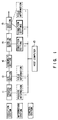
- FIG. 1 shows the intelligent test line system of the present invention.
- various information obtained by a process section 11 and a D/S section 12 is processed by a host computer 13 to add a quality rank to a wafer or a wafer lot, and a test condition in a burn-in section 14 and a test section 15 is determined on the basis of the quality rank.
- Process information (including trouble information) is obtained by the process section 11 and input to the host computer 13.
- Yield information is obtained by the D/S section 12 and input to the host computer 13.
- the host computer 13 adds a rank to a product (a wafer or a wafer lot) on the basis of the process information and the yield information.
- the host computer 13 determines a test condition in the burn-in section 14 and the test section 15 in accordance with the rank of the product, and transfers the test condition to the burn-in section 14 and the test section 15. This test condition changes with a change in the rank of a product.
- the burn-in section 14 and the test section 15 test the product under the test condition corresponding to the product to be tested.
- a quality rank is determined for each product (waver or wafer lot), and the test condition for each product is changed in accordance with the quality rank.
- a strict test condition is set for a poor-quality wafer, whereas a moderate test condition is set for a high-quality wafer, thereby shortening the test time as compared with the conventional system in which a test condition remains the same.
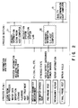
- FIGS. 2 and 3 show the detailed arrangement of the system of the present invention.
- Information for determining the condition of a burn-in test is constituted by primary information about an IC manufacturing process in a clean room and secondary information about an yield.
- the primary information is input to the host computer 13 via a clean room host computer 21.
- the secondary information is input to the host computer 13 via a D/S host computer 22.
- the primary information is information about the performance of the clean room. This information is a factor dominating the basic characteristics of a wafer lot. Therefore, it is considered that the distribution of quality ranks based on the primary information almost coincides with a normal distribution.
- products e.g., lots
- quality grades on the basis of the primary information:
- stress conditions of on-wafer-stress tests are preferably classified into two groups in accordance with the above four quality grades for the following reason.
- a stress condition similar to that in the conventional system is set for A and B ranks regarded as relatively high ranks, whereas a strict stress condition is set for C and D ranks regarded as low ranks, thereby degrading defective products in the early stage and removing them in a D/S step as the next step.
- This processing is advantageous in terms of economical efficiency and quality assurance.
- the secondary information is information about a D/S step of determining the quality of each chip in a wafer having undergone a process. This information is regarded as a factor for monitoring the initial quality of a lot and is used to verify the quality rank of a lot which is classified on the basis of the primary information. As this information, yield information is generally used.
- products e.g., lots
- products are classified into the following three quality grades on the basis of the secondary information:
- Table 1 shows the quality grades of lots in the form of a matrix by combining the ranks of the products based on the primary information and the ranks of the products based on the secondary information.
- products e.g., lots
- quality grades e.g., grades
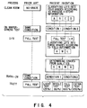
- FIG. 4 shows comparison between the conventional system and the system of the present invention.
- an on-wafer-stress test on, e.g., products (e.g., wafers) of A and B ranks is performed under condition 1
- the same test on products of C and D ranks is performed under condition 2.
- a "plus something (+°)" test (full test) is additionally conducted on products of quality rank D based on the primary information in a D/S step. Products determined as defective products by the full test in the D/S step are removed.
- a burn-in test is conducted on products of G and N ranks under condition 1, and the same test is conducted on products of W and A ranks under condition 2.
- the total test time in a test step is set to be 25% of that in the conventional system with respect to G rank; 60% with respect to N rank; 100% with respect to W rank; and 150% with respect to A rank.
- This test time is variously changed depending on the type of a product and the degree of difficulty of a manufacturing process.
- the test time is also changed depending on the degree of manufacturing skill.
- two conditions are set as burn-in conditions.
- three or more conditions e.g., a condition for each grade, may be set.
- Final test results are statistically processed by the host computer. That is, the burn-in conditions and the test conditions are always reexamined on the basis of quality ranks or test conditions and the actual quality of products.
- Table 2 shows the ratios of lots (of DRAMs in this case) classified on the basis of the primary information and the secondary information.
- a 50% B 30% C 15% D 5% H 50% G 25% G 15% N 7% W 3% M 35% G 17% N 10% W 5% A 2% L 15% N 8% W 5% A 2%
- the lots of A rank were 50%; the lots of B ranks, 30%; the lots of C rank, 15%; and the lots of D rank, 5%.
- the lots of H rank were 50%; the lots of M rank, 35%; and the lots of L rank, 15%.
- the lots of G rank are 57%; the lots of N rank, 25%; the lots of W rank, 13%; and the lots of A rank, 5%.
- Test times in the present invention are calculated with the test time in the conventional system being considered to be "1".
- the test time for the lots of G rank is 1/4 that in the conventional system (0.25); the test time for the lots of N rank, 3/5 (0.6); the test time for the lots of W rank, the same as that in the conventional system (1); and the test time for the lots of A rank, 1.5 times (1.5).
- the test time for products can be greatly reduced.
- the test time is about 50% of the test time in the conventional system, as indicated by equation (1), which corresponds to an efficient improvement of 200%. That is, with test facilities of the same size, products twice as many as those in the conventional system can be tested, and the production twice that in the conventional system can be ensured.
- the test cost is proportional to the test time, the test cost for products can be reduced, resulting in a great contribution to an increase in profit.
- this intelligent test line system is introduced into a new plant to be constructed.
- the facilities for tests and burn-in tests can be reduced by several 10%.
- the facility investment can be reduced accordingly, and hence the cost can be reduced.
- the facilities can be reduced in size, the space for the test facilities in the plan can also be reduced, resulting in a reduction in construction cost.
Landscapes
- Physics & Mathematics (AREA)
- General Physics & Mathematics (AREA)
- Testing Of Individual Semiconductor Devices (AREA)
- Testing Or Measuring Of Semiconductors Or The Like (AREA)
Claims (6)
- Verfahren zum Herstellen von integrierten Schaltungen, die folgenden Schritte in der gegebenen Reihenfolge umfassend:Verarbeiten einer Vielzahl von Wavern, um darauf IC-Chips zu bilden und Sammeln primärer Information bezüglich der Qualität des Prozesses, dem jeder Waver unterzogen wurde;Bewerten der Vielzahl von IC-Chips auf jedem Waver, um sekundäre Information bezüglich der Qualität jedes Chips zu erhalten;Bestimmen der Burn-in-Bedingung und der Post-burn-in-Testbedingung für jeden Waver auf Grundlage der primären Information und der sekundären Information, wobei die Waver in eine Vielzahl von Qualitätsrangordnungen (G, N, W, A) klassifiziert werden, in Übereinstimmung mit einer kombinierten Qualitätsbewertung, bestimmt durch ein Kombinieren der für jeden Waver aus der primären Information angezeigten Qualität und der durch die sekundäre Information angezeigten Qualität, und die Burn-in- und Post-burn-in-Testbedingungen werden so ausgewählt, daß sie für Waver mit niedrigerer Qualitätsrangordung strenger sind, bei denen die primäre Information anzeigt, daß die Qualität des Verarbeitungsschrittes schlecht war, und die sekundäre Information anzeigt, daß die Chip-Qualität niedrig ist, und werden so ausgewählt, daß sie für Waver mit höherer Qualitätsrangordnug moderater sind, bei denen die primäre Information anzeigt, daß die Qualität des Verarbeitungsschrittes gut war und die sekundäre Information anzeigt, daß die Chip-Qualität gut ist;Aufbau eines IC-Produktes aus einem IC-Chip;Durchführen eines Burn-in mit dem IC-Produkt in Übereinstimmung mit der festgelegten Burn-in-Bedingung; undTesten des IC-Produktes nach dem Burn-in in Übereinstimmung mit der festgelegten Post-burn-in-Testbedingung.
- Verfahren nach Anspruch 1, den zusätzlichen Schritt umfassend:Festlegen, auf Grundlage der primären Information, einer Auf-Waver-Belastungstestbedingung für jeden Waver nach einem Verarbeiten und vor einer Bewertung, undAnlegen einer Belastung durch eine vorbestimmte Temperatur und eine vorbestimmte Spannung an jeden Waver in Übereinstimmung mit der festgelegten Belastungsbedingung.
- Verfahren nach Anspruch 1, dadurch gekennzeichnet, daßdie primäre Information Information über die Bildung eines Films, Information über ein Ätzen, Information über ein Säubern und Information über eine Wärmebehandlung beinhaltet; unddie sekundäre Information Ausbeuteinformation einschließt.
- Verfahren nach Anspruch 1, dadurch gekennzeichnet, daßa) den Wavern ein erster (A, B, C, D) Qualitätsgrad auf Grundlage der primären Information zugeordnet wird, ein zweiter Qualitätsgrad (H, M, L) auf Grundlage der sekundären Information, und die Qualitätsrangordnung durch eine Kombination des ersten und des zweiten Qualitätsgrades bestimmt wird;b) die Burn-in- und Post-burn-in-Testbedingungen als tertiäre Information für die Burn-in- oder die Post-burn-in-Testschritte geliefert werden.
- Verfahren nach Anspruch 2, dadurch gekennzeichnet, daß die primäre Information Information über die Bildung eines Films, Information über Ätzen, Information über ein Säubern und Information über eine Wärmebehandlung beinhaltet.
- Ein intelligentes Testreihensystem zum Ausführen des Verfahrens nach Anspruch 1, umfassend:eine Verarbeitungsvorrichtung (11) zum Verarbeiten eines Wavers;eine Bewertungsvorrichtung (12), um eine Vielzahl von auf dem Waver durch die Verarbeitungsvorrichtung hergestellten IC-Chips zu bewerten;eine Steuervorrichtung (13) mit einem ersten Eingang, der mit der Verarbeitungsvorrichtung verbunden ist, um primäre Information bezüglich der Qualität des Verarbeitens zu empfangen, und mit einem zweiten Input, der mit der Bewertungsvorrichtung verbunden ist, um sekundäre Information bezüglich der Qualität der IC-Chips zu empfangen und um eine Burn-in-Bedingung und eine Post-burn-in-Testbedingung für jeden Waver auf Grundlage der von der Verarbeitungsvorrichtung erhaltenen primären Information und der von der Bewertungsvorrichtung erhaltenen sekundären Information einzustellen;eine Montagevorrichtung (16), um ein IC-Produkt aus jedem IC-Chip aufzubauen;eine Burn-in-Vorrichtung (14), um ein Burn-in mit dem IC-Chip auf dem Waver oder dem IC-Produkt unter der Burn-in-Bedingung durchzuführen; undeine Post-burn-in-Testvorrichtung (15), um den IC-Chip oder das IC-Produkt nach dem Burn-in unter der Post-burn-in-Testbedingung zu testen.
Applications Claiming Priority (2)
| Application Number | Priority Date | Filing Date | Title |
|---|---|---|---|
| JP313404/93 | 1993-12-14 | ||
| JP05313404A JP3099932B2 (ja) | 1993-12-14 | 1993-12-14 | インテリジェントテストラインシステム |
Publications (3)
| Publication Number | Publication Date |
|---|---|
| EP0660385A2 EP0660385A2 (de) | 1995-06-28 |
| EP0660385A3 EP0660385A3 (de) | 1996-06-05 |
| EP0660385B1 true EP0660385B1 (de) | 1999-06-02 |
Family
ID=18040869
Family Applications (1)
| Application Number | Title | Priority Date | Filing Date |
|---|---|---|---|
| EP94119756A Expired - Lifetime EP0660385B1 (de) | 1993-12-14 | 1994-12-14 | Intelligente Prüfungsstrasse |
Country Status (5)
| Country | Link |
|---|---|
| US (1) | US5635850A (de) |
| EP (1) | EP0660385B1 (de) |
| JP (1) | JP3099932B2 (de) |
| KR (1) | KR0164247B1 (de) |
| DE (1) | DE69418841T2 (de) |
Families Citing this family (18)
| Publication number | Priority date | Publication date | Assignee | Title |
|---|---|---|---|---|
| US5716856A (en) * | 1995-08-22 | 1998-02-10 | Advanced Micro Devices, Inc. | Arrangement and method for detecting sequential processing effects in manufacturing using predetermined sequences within runs |
| JP3691195B2 (ja) * | 1997-02-13 | 2005-08-31 | 株式会社ルネサステクノロジ | 半導体装置の製造方法 |
| US6594598B1 (en) * | 1997-10-08 | 2003-07-15 | Matsushita Electronics Corporation | Method for controlling production line |
| FR2790833B1 (fr) * | 1999-03-08 | 2001-04-20 | St Microelectronics Sa | Procede de test statistique de circuits integres |
| JP3844912B2 (ja) * | 1999-06-10 | 2006-11-15 | 富士通株式会社 | 半導体記憶装置の試験方法及び試験装置と半導体記憶装置 |
| US6319737B1 (en) * | 1999-08-10 | 2001-11-20 | Advanced Micro Devices, Inc. | Method and apparatus for characterizing a semiconductor device |
| US7194366B2 (en) | 2001-10-19 | 2007-03-20 | Auburn University | System and method for estimating reliability of components for testing and quality optimization |
| US6915177B2 (en) | 2002-09-30 | 2005-07-05 | Advanced Micro Devices, Inc. | Comprehensive integrated lithographic process control system based on product design and yield feedback system |
| US7340359B2 (en) * | 2005-05-02 | 2008-03-04 | Optimaltest Ltd | Augmenting semiconductor's devices quality and reliability |
| KR101250234B1 (ko) * | 2005-12-29 | 2013-04-05 | 엘지디스플레이 주식회사 | 액정표시소자 검사시스템 및 방법, 이를 이용한액정표시소자 제조방법 |
| US8299809B2 (en) * | 2009-09-21 | 2012-10-30 | International Business Machines Corporation | In-line characterization of a device under test |
| JP5554750B2 (ja) * | 2011-06-15 | 2014-07-23 | 富士通テレコムネットワークス株式会社 | 試験管理装置 |
| JP6483373B2 (ja) * | 2014-08-07 | 2019-03-13 | 株式会社東芝 | 生産支援システムおよび生産支援方法 |
| JP5956094B1 (ja) * | 2015-03-10 | 2016-07-20 | 三菱化学エンジニアリング株式会社 | 製造プロセスの解析方法 |
| JP2018006603A (ja) * | 2016-07-04 | 2018-01-11 | 富士通株式会社 | システム、および試験決定方法 |
| JP6716423B2 (ja) * | 2016-10-26 | 2020-07-01 | 三菱ケミカルエンジニアリング株式会社 | 生産プロセスの解析方法 |
| JP6549760B1 (ja) * | 2018-06-26 | 2019-07-24 | 三菱ケミカルエンジニアリング株式会社 | 生産システム、生産方法、及び制御装置 |
| JP6481916B1 (ja) * | 2018-06-26 | 2019-03-13 | 三菱ケミカルエンジニアリング株式会社 | 生産システム、生産方法及び制御装置 |
Family Cites Families (11)
| Publication number | Priority date | Publication date | Assignee | Title |
|---|---|---|---|---|
| US3344351A (en) * | 1963-06-03 | 1967-09-26 | Gen Instrument Corp | Testing apparatus for a sequence of transistors and the like having a condition responsive marker |
| JPS60254626A (ja) * | 1984-05-30 | 1985-12-16 | Sharp Corp | ウエハテスト方法 |
| US4931722A (en) * | 1985-11-07 | 1990-06-05 | Control Data Corporation | Flexible imbedded test system for VLSI circuits |
| JPH0616475B2 (ja) * | 1987-04-03 | 1994-03-02 | 三菱電機株式会社 | 物品の製造システム及び物品の製造方法 |
| US5093982A (en) * | 1987-06-01 | 1992-03-10 | Reliability Incorporated | Automated burn-in system |
| US4985988A (en) * | 1989-11-03 | 1991-01-22 | Motorola, Inc. | Method for assembling, testing, and packaging integrated circuits |
| JPH0425349A (ja) * | 1990-05-21 | 1992-01-29 | Mitsubishi Electric Corp | 混成ロット編成方法及び装置 |
| JP2925337B2 (ja) * | 1990-12-27 | 1999-07-28 | 株式会社東芝 | 半導体装置 |
| CA2073886A1 (en) * | 1991-07-19 | 1993-01-20 | Tatsuya Hashinaga | Burn-in apparatus and method |
| CA2073916A1 (en) * | 1991-07-19 | 1993-01-20 | Tatsuya Hashinaga | Burn-in apparatus and method |
| US5539652A (en) * | 1995-02-07 | 1996-07-23 | Hewlett-Packard Company | Method for manufacturing test simulation in electronic circuit design |
-
1993
- 1993-12-14 JP JP05313404A patent/JP3099932B2/ja not_active Expired - Fee Related
-
1994
- 1994-12-14 US US08/355,538 patent/US5635850A/en not_active Expired - Fee Related
- 1994-12-14 KR KR1019940034066A patent/KR0164247B1/ko not_active Expired - Fee Related
- 1994-12-14 DE DE69418841T patent/DE69418841T2/de not_active Expired - Fee Related
- 1994-12-14 EP EP94119756A patent/EP0660385B1/de not_active Expired - Lifetime
Also Published As
| Publication number | Publication date |
|---|---|
| DE69418841D1 (de) | 1999-07-08 |
| DE69418841T2 (de) | 1999-10-21 |
| EP0660385A3 (de) | 1996-06-05 |
| JPH07167911A (ja) | 1995-07-04 |
| KR950019754A (ko) | 1995-07-24 |
| KR0164247B1 (ko) | 1999-03-20 |
| JP3099932B2 (ja) | 2000-10-16 |
| EP0660385A2 (de) | 1995-06-28 |
| US5635850A (en) | 1997-06-03 |
Similar Documents
| Publication | Publication Date | Title |
|---|---|---|
| EP0660385B1 (de) | Intelligente Prüfungsstrasse | |
| US6789032B2 (en) | Method of statistical binning for reliability selection | |
| US7529634B2 (en) | Method, apparatus, and computer program of searching for clustering faults in semiconductor device manufacturing | |
| US5862055A (en) | Automatic defect classification individual defect predicate value retention | |
| US6365860B1 (en) | Method for sorting integrated circuit devices | |
| US6788993B2 (en) | Sorting a group of integrated circuit devices for those devices requiring special testing | |
| US6523144B2 (en) | Intelligent binning for electrically repairable semiconductor chips and method | |
| US20030120457A1 (en) | System and method for estimating reliability of components for testing and quality optimization | |
| US8126681B2 (en) | Semiconductor outlier identification using serially-combined data transform processing methodologies | |
| US5935264A (en) | Method and apparatus for determining a set of tests for integrated circuit testing | |
| US6577972B2 (en) | Sampling inspection managing system | |
| US6963213B1 (en) | Auto-recovery wafer testing apparatus and wafer testing method | |
| US6499118B1 (en) | Redundancy analysis method and apparatus for ATE | |
| US7035770B2 (en) | Fuzzy reasoning model for semiconductor process fault detection using wafer acceptance test data | |
| US7587292B2 (en) | Method of monitoring a semiconductor manufacturing trend | |
| US7496478B2 (en) | Method of monitoring a semiconductor manufacturing trend | |
| US6847855B2 (en) | Method for fault analysis in wafer production | |
| US6906969B2 (en) | Hybrid fuses for redundancy | |
| KR100525103B1 (ko) | 웨이퍼 비지니스 에스비엘 방법 | |
| JP3012242B2 (ja) | 半導体集積回路の製造方法 | |
| Hirase | Study on the costs of on-site VLSI testing | |
| Kiel et al. | Strategy for a flexible and inexpensive defect density line monitoring for microchip manufacturing | |
| US20030027362A1 (en) | Method for determining deficient processes and deficient processing stations | |
| Wang et al. | Analyzing alternative strategies of semiconductor final testing | |
| JP2969822B2 (ja) | 半導体装置の製造管理システム |
Legal Events
| Date | Code | Title | Description |
|---|---|---|---|
| PUAI | Public reference made under article 153(3) epc to a published international application that has entered the european phase |
Free format text: ORIGINAL CODE: 0009012 |
|
| 17P | Request for examination filed |
Effective date: 19941214 |
|
| AK | Designated contracting states |
Kind code of ref document: A2 Designated state(s): DE FR GB |
|
| PUAL | Search report despatched |
Free format text: ORIGINAL CODE: 0009013 |
|
| AK | Designated contracting states |
Kind code of ref document: A3 Designated state(s): DE FR GB |
|
| 17Q | First examination report despatched |
Effective date: 19961209 |
|
| GRAG | Despatch of communication of intention to grant |
Free format text: ORIGINAL CODE: EPIDOS AGRA |
|
| GRAG | Despatch of communication of intention to grant |
Free format text: ORIGINAL CODE: EPIDOS AGRA |
|
| GRAH | Despatch of communication of intention to grant a patent |
Free format text: ORIGINAL CODE: EPIDOS IGRA |
|
| GRAH | Despatch of communication of intention to grant a patent |
Free format text: ORIGINAL CODE: EPIDOS IGRA |
|
| GRAA | (expected) grant |
Free format text: ORIGINAL CODE: 0009210 |
|
| AK | Designated contracting states |
Kind code of ref document: B1 Designated state(s): DE FR GB |
|
| RAP1 | Party data changed (applicant data changed or rights of an application transferred) |
Owner name: TOSHIBA MICRO-ELECTRONICS CORPORATION Owner name: KABUSHIKI KAISHA TOSHIBA |
|
| REF | Corresponds to: |
Ref document number: 69418841 Country of ref document: DE Date of ref document: 19990708 |
|
| ET | Fr: translation filed | ||
| PLBE | No opposition filed within time limit |
Free format text: ORIGINAL CODE: 0009261 |
|
| STAA | Information on the status of an ep patent application or granted ep patent |
Free format text: STATUS: NO OPPOSITION FILED WITHIN TIME LIMIT |
|
| 26N | No opposition filed | ||
| REG | Reference to a national code |
Ref country code: GB Ref legal event code: IF02 |
|
| PGFP | Annual fee paid to national office [announced via postgrant information from national office to epo] |
Ref country code: GB Payment date: 20071212 Year of fee payment: 14 Ref country code: FR Payment date: 20071210 Year of fee payment: 14 |
|
| PGFP | Annual fee paid to national office [announced via postgrant information from national office to epo] |
Ref country code: DE Payment date: 20071206 Year of fee payment: 14 |
|
| GBPC | Gb: european patent ceased through non-payment of renewal fee |
Effective date: 20081214 |
|
| REG | Reference to a national code |
Ref country code: FR Ref legal event code: ST Effective date: 20090831 |
|
| PG25 | Lapsed in a contracting state [announced via postgrant information from national office to epo] |
Ref country code: DE Free format text: LAPSE BECAUSE OF NON-PAYMENT OF DUE FEES Effective date: 20090701 |
|
| PG25 | Lapsed in a contracting state [announced via postgrant information from national office to epo] |
Ref country code: GB Free format text: LAPSE BECAUSE OF NON-PAYMENT OF DUE FEES Effective date: 20081214 |
|
| PG25 | Lapsed in a contracting state [announced via postgrant information from national office to epo] |
Ref country code: FR Free format text: LAPSE BECAUSE OF NON-PAYMENT OF DUE FEES Effective date: 20081231 |