EP0660387A2 - Methode und Apparat zur Messung der Oxidladung auf Halbleiterscheiben - Google Patents
Methode und Apparat zur Messung der Oxidladung auf Halbleiterscheiben Download PDFInfo
- Publication number
- EP0660387A2 EP0660387A2 EP94480157A EP94480157A EP0660387A2 EP 0660387 A2 EP0660387 A2 EP 0660387A2 EP 94480157 A EP94480157 A EP 94480157A EP 94480157 A EP94480157 A EP 94480157A EP 0660387 A2 EP0660387 A2 EP 0660387A2
- Authority
- EP
- European Patent Office
- Prior art keywords
- needle
- dielectric layer
- pressure
- needle tip
- probe
- Prior art date
- Legal status (The legal status is an assumption and is not a legal conclusion. Google has not performed a legal analysis and makes no representation as to the accuracy of the status listed.)
- Granted
Links
Images

Classifications
-
- G—PHYSICS
- G01—MEASURING; TESTING
- G01R—MEASURING ELECTRIC VARIABLES; MEASURING MAGNETIC VARIABLES
- G01R31/00—Arrangements for testing electric properties; Arrangements for locating electric faults; Arrangements for electrical testing characterised by what is being tested not provided for elsewhere
- G01R31/12—Testing dielectric strength or breakdown voltage ; Testing or monitoring effectiveness or level of insulation, e.g. of a cable or of an apparatus, for example using partial discharge measurements; Electrostatic testing
- G01R31/1227—Testing dielectric strength or breakdown voltage ; Testing or monitoring effectiveness or level of insulation, e.g. of a cable or of an apparatus, for example using partial discharge measurements; Electrostatic testing of components, parts or materials
- G01R31/1263—Testing dielectric strength or breakdown voltage ; Testing or monitoring effectiveness or level of insulation, e.g. of a cable or of an apparatus, for example using partial discharge measurements; Electrostatic testing of components, parts or materials of solid or fluid materials, e.g. insulation films, bulk material; of semiconductors or LV electronic components or parts; of cable, line or wire insulation
- G01R31/129—Testing dielectric strength or breakdown voltage ; Testing or monitoring effectiveness or level of insulation, e.g. of a cable or of an apparatus, for example using partial discharge measurements; Electrostatic testing of components, parts or materials of solid or fluid materials, e.g. insulation films, bulk material; of semiconductors or LV electronic components or parts; of cable, line or wire insulation of components or parts made of semiconducting materials; of LV components or parts
-
- G—PHYSICS
- G01—MEASURING; TESTING
- G01R—MEASURING ELECTRIC VARIABLES; MEASURING MAGNETIC VARIABLES
- G01R1/00—Details of instruments or arrangements of the types included in groups G01R5/00 - G01R13/00 and G01R31/00
- G01R1/02—General constructional details
- G01R1/06—Measuring leads; Measuring probes
- G01R1/067—Measuring probes
- G01R1/06711—Probe needles; Cantilever beams; "Bump" contacts; Replaceable probe pins
- G01R1/06733—Geometry aspects
- G01R1/06738—Geometry aspects related to tip portion
-
- H—ELECTRICITY
- H10—SEMICONDUCTOR DEVICES; ELECTRIC SOLID-STATE DEVICES NOT OTHERWISE PROVIDED FOR
- H10P—GENERIC PROCESSES OR APPARATUS FOR THE MANUFACTURE OR TREATMENT OF DEVICES COVERED BY CLASS H10
- H10P74/00—Testing or measuring during manufacture or treatment of wafers, substrates or devices
- H10P74/20—Testing or measuring during manufacture or treatment of wafers, substrates or devices characterised by the properties tested or measured, e.g. structural or electrical properties
- H10P74/207—Electrical properties, e.g. testing or measuring of resistance, deep levels or capacitance-voltage characteristics
-
- Y—GENERAL TAGGING OF NEW TECHNOLOGICAL DEVELOPMENTS; GENERAL TAGGING OF CROSS-SECTIONAL TECHNOLOGIES SPANNING OVER SEVERAL SECTIONS OF THE IPC; TECHNICAL SUBJECTS COVERED BY FORMER USPC CROSS-REFERENCE ART COLLECTIONS [XRACs] AND DIGESTS
- Y10—TECHNICAL SUBJECTS COVERED BY FORMER USPC
- Y10T—TECHNICAL SUBJECTS COVERED BY FORMER US CLASSIFICATION
- Y10T29/00—Metal working
- Y10T29/49—Method of mechanical manufacture
- Y10T29/49002—Electrical device making
Definitions
- the present invention generally relates to a method and apparatus for measurement of electrical properties in a semiconductor wafer, and more particularly, to the measurement of the electrical properties of a dielectric layer on a semiconductor wafer.
- the determination of electrical properties of a dielectric layer on a semiconductor wafer body is a critical factor in the production of such wafers as is well known in the art. Measurements such as dielectric rupture voltage, dielectric field strength, time dependent dielectric breakdown and oxide charge measurements, for example, are typically accomplished by first fabricating metal or doped polysilicon mesas over the dielectric layer that serve as electrical contacts to which measurement probes may be applied.
- MOS metal-oxide-semiconductor
- any oxide on the back side of the wafer must first be stripped from the back side of the wafer before the back side aluminum evaporation.
- a metal mask with an array of various size apertures is positioned immediately in front of the wafer to determine where dots will be formed during aluminum evaporation.
- a sintering and alloying process is then completed to reduce interface states charge at the oxide/silicon interface and to reduce contact resistance between the back side aluminum and silicon.
- Another disadvantage of this technique is its invasiveness within the wafer structure, resulting in inaccuracies being introduced in electrical measurements.
- MOS Capacitance-Voltage (C-V) measurements are very useful for fixed, mobile, and surface states charge characterization; however, for a variety of charge measurement requirements, the conventional MOS method can be prohibitively expensive and inconvenient.
- sample preparation typically includes frontside aluminum dots and backside blanket aluminum. Such sample preparation is costly, time consuming and destructive.
- MOS charge monitoring on product wafers a highly desirable feature, such as being able to test arbitrary locations at almost any stage of processing, is not a practical possibility.
- the geometry and operating conditions of the '561 metal POS probe includes an extremely flat geometry and a relatively low, non-deforming pressure on the order of 10 psi., the low pressure being a proper pressure for avoiding damage of the test sample surface.
- the flat geometry of the '561 metal POS probe presents a sharp edge, which if excessive force were applied to the probe in contacting the dielectric, would increase the probability for damage and cracking to occur in the dielectric layer.
- the '561 metal POS probe is not well suited.
- the effective air gap between the '561 probe tip and the dielectric surface would need to be less than 0.3 nm for a C-V characteristic to have less than a 10% error.
- a higher pressure may be applied to close up any small air gaps; however, the resultant stress near the sharp edge of the flat probe greatly increases the likelihood of surface damage to the test sample.
- the '561 POS test probe involves a polishing process, not subject to high repeatability, for use in making the same, and thus results in increased variations between probes.
- An object of the present invention is to provide a improved POS probe, and a method of making the same, for overcoming the above-mentioned disadvantages in the art.
- Another object of the present invention is to provide a POS probe, and method of making the same, for improved POS measurements through improved coupling to a dielectric being measured.
- a probe, and method of making the same, suitable for Probe-Oxide-Semiconductor (POS) electrical characterization measurements of a dielectric layer on a semiconductor substrate comprises an electrically conductive probe needle, the needle having a rounded tip end of a first radius, the rounded tip end further being suitable for undergoing a plastic deformation.
- the needle is positioned above the dielectric layer on the semiconductor substrate and the needle tip forced down onto the smooth surface of the dielectric layer in a controlled manner for causing the needle tip to undergo a plastic deformation in which an outer portion of the rounded tip end is maintained at the first radius and an inner portion of the rounded tip end is increased to a second radius, the second radius being larger than the first.
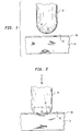
- the method according to the present invention for forming a probe suitable for POS electrical characterization measurements begins with providing an electrically conductive probe needle 10.
- the needle 10 is characterized by a rounded tip end 12 of a first radius of curvature R1, the rounded tip end 12 being suitable for undergoing a desired plastic deformation, i.e., a permanent deformation, as will be explained in further detail hereinbelow.
- the needle 10 preferably comprises a stable, corrosion resistant, metal and further having mechanical properties that provide for plastic deformation.
- Such a needle can comprise a tungsten probe needle, such as are commercially available from Moser Jewel Company of Perth Amboy, New Jersey.
- Typical dimensions for needle 10 may comprise, for instance, a length dimension on the order of one (1) inch, a cross-sectional dimension on the order of a twenty-eight (28) mil diameter along a major portion thereof, a tapered section having a taper on the order of ten (10) degrees, and a round tip with a radius of curvature on the order of one-half (0.5) mils (or as expressed in microns, 12.5 ⁇ m).
- Other dimensions suitable to the requirements of a particular POS measurement application, may be used as necessary. It should be noted that present commercially available tungsten probe needles are inadequate for the purposes of performing POS electrical characterization measurements, that is, they perform poorly due to their non-optimal shape, as will be subsequently discussed.
- an optimal shape comprises a needle tip having a radius of curvature that is first large, over a short arc, and then rapidly changes to a small radius of curvature with increasing arc.
- the end portion of the needle tip, having a large radius of curvature is used for making intimate, highly conformal contact with the dielectric layer of interest.
- the much smaller radius of curvature of the needle tip rapidly curves away from the dielectric layer of interest (i.e., the semiconductor surface) in order to create a well defined intimate contact area and further provide for accurate POS measurements, discussed supra.
- needle 10 is advantageously conditioned according to the following. Needle 10 is positioned above a semiconductor substrate 14.
- Substrate 14 may comprise any suitable substrate, capable of elastic deformation (i.e., non-permanent deformation), such as a silicon substrate.
- dielectric layer 16 On a top surface of substrate 14 is a dielectric layer 16, dielectric layer 16 comprising a thermal oxide layer, for example.
- Dielectric layer 16 is further characterized by a relatively smooth top surface 15.
- Semiconductor substrates and dielectric layers are well known in the art and thus not discussed in great detail herein.
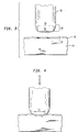
- needle 10 is positioned above substrate 14, such that the rounded tip 12 is proximate to surface 15 of dielectric layer 16. Thereafter, needle 10 is forced down onto the smooth surface 15 of the dielectric layer 16 in a controlled manner for causing the needle tip 12 to undergo a desired plastic deformation (or permanent deformation) in which an outer portion 18 of the rounded tip end 12 is maintained at the first radius R1 and an inner portion 20 of the rounded tip end 12 is increased to a second radius R2, the second radius R2 being larger than the first radius R1.
- needle 10 is positioned substantially perpendicular to the top surface 15 and the semiconductor substrate 14. Needle tip end 12 is slowly and gently lowered down and brought into contact with the dielectric layer 16, and thereafter forced down onto dielectric layer 16 with a force sufficient for developing a conditioning pressure (i.e., plastic deformation pressure) to provide the desired conditioning of the probe needle 10 (i.e., plastic deformation).
- a conditioning pressure i.e., plastic deformation pressure
- the conditioning pressure developed between probe needle 10 and the dielectric layer 16/substrate 14 structure combination must be sufficient for causing needle tip 12 to undergo the desired plastic deformation, that is, corresponding to a pressure for forming the inner portion 20 of probe tip 12 to have a desired radius, while maintaining the outer portion 18 at the first radius.
- the force sufficient for developing the conditioning pressure is applied in such a manner as to avoid fracturing of the probe tip 12 while enabling the desired plastic deformation thereof to occur.
- a force F1 is applied to probe 10, the force F1 being sufficient so as to develop the conditioning pressure comprising a pressure in a range from a first pressure to a second pressure.
- force F1 comprises an increasing force, from a first force to a second force, corresponding to a range on the order of 0.001-0.016 pounds (i.e., 0.01-7.3 grams).
- Force F1 is sufficient to provide a conditioning pressure in the range from a first pressure on the order of 0-100 psi to a second pressure on the order of 100,000-150,000 psi.
- the second pressure is, more preferably, on the order of 130,000 psi.
- the force F1 is applied in a gradual manner, that is, gradually from the first force to the second force, whereby pressure is gradually developed, beginning from the first pressure and increasing to the second pressure, at a controlled rate to avoid fracturing of the probe tip 12.
- Force F1 may be gradually increased in either a continuous manner or an incremental manner. In the continuous manner, the force is continuously increased at a slow rate. In the incremental manner, the force is incrementally increased, for example, in increments of approximately 0.0008 pounds, at a slow rate.
- a gradual increase in the applied force F1 is highly desirable since material comprising the probe tip 12 must absorb and/or relieve the pressure applied as a result of the force F1, and additionally, at the rate at which force F1 is applied. That is, the material comprising probe tip 12 undergoes a material or molten flow to relieve the pressure applied as a result of force F1. If the material comprising probe tip 12 is stressed beyond it's ability to flow, a rupture or fracture in the probe tip 12 can occur. Thus, the force F1 is selected so as to substantially reduce any excessive shock to the probe tip 12 material, thereby avoiding probe tip 12 material fracture.
- the dielectric layer 16 and the substrate 14 undergo a limited amount of elastic or temporary deformation during the conditioning of probe 10, and more particularly, conditioning of probe tip 12, as shown in FIG. 2. This is due in part because of the somewhat elastic nature of the dielectric layer 16 and substrate 14.
- the limited temporary deformation is primarily due to the high pressure contact (i.e., over a small contact area) with the relatively stiffer needle tip 12.
- Solid materials are composed of atoms that are held together by bonds that behave as microscopic springs. Elastic behavior of various materials can be described by materials constants that relate stress (applied pressure) to strain (change in physical dimensions due to stress). Young's Modulus, Y, is one such constant.
- the probe tip comprising tungsten is relatively much stiffer than the silicon substrate (i.e., the tungsten probe tip having about a three times higher Young's Modulus than silicon).
- the probe tip 12 comprises an optimal shape for POS electrical characteristic measurements. That is, the tip 12 has a much larger radius of curvature, on the order of 135 mils (or as expressed in microns, 3,500 ⁇ m), for example, and is partially work hardened for increased mechanical stability.
- the conditioned probe 10 provides a good compromise between 1) the small area needed for a high pressure, intimate contact and 2) a large enough area necessary for minimizing electrical noise in POS measurements.
- POS apparatus 100 for producing a POS probe according to the method described above, will now be described with reference to FIG. 5 and further in accordance with the present invention.
- POS apparatus 100 further provides for electrical characterization measurements of a dielectric layer 16 on a semiconductor substrate 14 utilizing the POS probe of the present invention.
- POS apparatus 100 comprises a means 110 for supporting the semiconductor substrate in a prescribed position, such as any well known suitable conductive semiconductor wafer chuck.
- a first suitable contact means 112 electrically contacts the substrate 14 and substrate support means 110.
- a suitable means 114 such as a non-conductive clamp, is provided for receiving electrically conductive probe needle 10, and preferably to position probe needle 10 substantially perpendicular to the semiconductor substrate 14.
- Probe needle 10 when unconditioned, comprises a needle having a rounded tip end of a first radius, the rounded tip end further being suitable for undergoing a plastic deformation as discussed hereinabove.
- a means 116 is electrically connected between said first contacting means 112 and the probe needle 10.
- Means 118 provides an electrical characterization measurement, representative of an electrical characteristic of the dielectric layer 16, such as a capacitance-voltage measurement, when the probe needle 10 is in electrical contact with the dielectric layer as will be further discussed hereinbelow.
- Electrical characterization measurement means 116 comprises an AC generator 118 for providing an AC output signal to wafer chuck 110 and substrate 14 via electrical contact means 112.
- AC generator may comprise any suitably known generator.
- AC generator 118 is further connected to lock-in amplifier 120 for providing a synchronous AC output signal from AC generator 118 to a synchronous input of lock-in amplifier 120.
- Lock-in amplifier 120 may comprise any suitably known lock-in amplifier.
- Electrical characterization means 116 further comprises a circuit network of resistor R1, capacitor C, and resistor R2, electrically connected to probe 10 at an opposite end from probe tip 12.
- a high impedance buffer 122 is further connected at one end thereof at a node between capacitor C and resistor R2 and is further connected at a second end thereof to lock-in amplifier 120.
- High impedance buffer 122 is placed close to the probe needle 10 to provide good signal-to-noise traces with respect to the relatively small POS capacitance values to be measured.
- Buffer 122 is electrically connected to a signal input of lock-in amplifier 120 to further enhance signal-to-noise.
- a DC ramp generator 124 is electrically connected to an opposite end of resistor R1 and further connected to an X-input of X-Y plotter 126.
- DC ramp generator 124 and X-Y plotter 126 may comprise any suitable DC ramp generator or X-Y plotter, respectively, known in the art.
- the signal output of lock-in amplifier 120 is connected to the Y-input of X-Y plotter 126.
- a positioning means 128 is mechanically connected to receiving means 114 for positioning receiving means 114 such that a probe needle 10 received therein is positioned above the dielectric layer 16 on the semiconductor substrate 14.
- Positioning means 128 can comprise, for example, any suitable mechanical means, such as a linear translation device having flexure arms 130 or flat springs attached thereto.
- positioning means 128 is electrically controllable. Translation of flexure arms 130 in a upward/downward movement, as indicated by arrow 132 in FIG. 5, effectively raises/lowers needle 10. Continued translation of flexure arms 130 downward, subsequent to needle 10 contacting dielectric layer 16, results in a force being applied to needle 10.
- the amount of deflection of flexure arms 130 is proportional to an amount of force applied to needle 10 upon dielectric layer 16, thus providing an indication of the amount of force being applied to needle 10. Any suitable means, such as a displacement transducer and appropriate electronic circuitry, may be used for measuring the amount of deflection of flexure arms 130.
- a control means 134 is electrically connected to positioning means 128 to control positioning means 128 to operate i) in a first mode of operation to condition the probe needle 10 and ii) in a second mode of operation for obtaining an electrical characterization measurement from the electrical characterization measurement means 116.
- Control means 134 is further electrically connected to lock-in amplifier 120 for receiving the output signal therefrom.
- Control means 134 can comprise any suitable controller, such as a computer or the like, the controller being programmed by known techniques for performing the desired functions as described herein.
- control means 134 controls positioning means 128 for providing a desired downward force.
- positioning means 128 is controlled by control means 134 to be operable in the first and second modes as follows.
- positioning means 128 forces the needle tip 12 down onto the smooth surface of the dielectric layer 16 in a first controlled manner for causing the needle tip 12 to undergo a plastic deformation in which an outer portion 18 of the rounded tip end 12 is maintained at the first radius R1 and an inner portion 20 of the rounded tip end 12 is increased to a second radius R2, the second radius being larger than the first.
- positioning means 128 forces the needle tip 12 down onto the smooth surface of the dielectric layer 16 in a second controlled manner for intimately and electrically contacting with the dielectric layer 16 within a contacting diameter D2, the contacting diameter D2 substantially on the order of the inner portion 20 (i.e., diameter D1) of the rounded tip end 12.
- the POS apparatus 100 operates in accordance with the present invention for conditioning a POS probe 10 and for effecting POS electrical characterization measurements as follows.
- an unconditioned probe needle in inserted into receiving means 114.
- Control means 134 controls positioning means 128 to bring the needle tip 12 gently into contact with the dielectric layer 16, and thereafter forces the needle tip 12 down onto the dielectric layer 16 with a force sufficient to develop a pressure over a range from a first pressure to a second pressure, whereby the needle tip undergoes a desired plastic deformation and is further work hardened thereby.
- the pressure is over a range from a first pressure on the order of 0-100 psi to a second pressure on the order of between 100,000-150,000 psi. More particularly, the second pressure is on the order of 130,000 psi.
- the force F1 applied is sufficient to gradually develop the pressure from the first pressure to the second pressure, wherein the second pressure is greater than the first.
- the applied force F1 may either be i) a continuously increasing force, i.e., continuously increasing from a first force to a second force, sufficient to gradually develop the pressure continuously from the first pressure to the second pressure, or ii) an incrementally increasing force, i.e., incrementally increasing from a first force to a second force, sufficient to gradually develop the pressure incrementally (in increments on the order of 5,000 to 10,000 psi for example) from the first pressure to the second pressure.
- Monitoring of an amount of the applied force to the probe needle 10 can be accomplished by monitoring an amount of deflection of flexure arms 130, as discussed above, the amount of deflection being proportional to the amount of force being applied.
- the monitored applied force provides feedback for use by control means 134 for controlling the positioning of positioning means 128.
- apparatus 100 For effecting POS electrical characterization measurements, apparatus 100 operates as follows.
- a conditioned POS probe 10, conditioned according to the above, is inserted into receiving means 114.
- Control means 134 controls positioning means 128 to be operable in a measurement mode for forcing the needle tip 12 down onto the smooth surface of the dielectric layer 16 in a controlled manner. Needle tip 12 is forced down onto the smooth surface of dielectric layer for intimately and electrically contacting with the dielectric layer within a contacting diameter D2 as shown in FIG. 4.
- the contacting diameter D2 is on the order of the inner portion 20 of the rounded tip end 12.
- positioning means 128 is controlled by control means 134 for bringing the needle tip 12 gently into contact with the dielectric layer 16, and thereafter forcing the needle tip 12 down onto the dielectric layer 16 with a force F2 sufficient to develop a pressure on the order of 20,000 psi.
- F2 force sufficient to develop a pressure on the order of 20,000 psi.
- the needle tip 12 is buried into the dielectric layer 16 and the surface of semiconductor substrate 14 within the contacting diameter D2. Because of the elastic nature of dielectric layer 16 and the underlying substrate 14, the dielectric layer and substrate return to their corresponding normal shapes upon retraction of the probe tip 12 from the surface of dielectric layer 16. That is, the elastic deformation limit of the dielectric layer and semiconductor wafer are not exceeded during the measurement mode.
- conditioned probe needle 10 An optimal contact for capacitance measurements is thus achieved using the conditioned probe needle 10 according to the present invention. Furthermore, the conditioned probe needle 10 is work hardened and thus does not undergo appreciable deformation during capacitance measurements, rather, the dielectric layer and underlying substrate undergo the deformation. Measurements taken using the present invention are thus very repeatable. In addition, a conditioned probe needle according to the present invention provides a lengthened useful lifetime.
- an electrical characterization measurement may be made, the measurement being similar to that using the conventional MOS measurement method.
- apparatus 100 may operate to condition a probe needle 10 in response to an electrical characterization measurement or measurements. That is, control means 134 may monitor a measured capacitance, between the probe tip 12 and the substrate 14, during the conditioning of the probe tip. In this instance, the measured capacitance would be compared with a desired capacitance, the desired capacitance corresponding to a known capacitance for a particular dielectric layer being used. In response to the measured capacitance, control means 134 can thus advantageously control positioning means 128 for providing force F1 for conditioning the probe needle 10, as discussed above.
- the method and apparatus of the present invention are well suited for providing a desired electrical characterization measurement of a dielectric layer upon a semiconductor substrate.
- the present invention further provides a method and apparatus for advantageously providing a highly conformal, well-defined, intimate contact for electrical characterization measurements.
Landscapes
- Physics & Mathematics (AREA)
- General Physics & Mathematics (AREA)
- Geometry (AREA)
- Measuring Leads Or Probes (AREA)
- Testing Or Measuring Of Semiconductors Or The Like (AREA)
- Tests Of Electronic Circuits (AREA)
- Testing Of Individual Semiconductor Devices (AREA)
Applications Claiming Priority (2)
| Application Number | Priority Date | Filing Date | Title |
|---|---|---|---|
| US173320 | 1993-12-22 | ||
| US08/173,320 US5500607A (en) | 1993-12-22 | 1993-12-22 | Probe-oxide-semiconductor method and apparatus for measuring oxide charge on a semiconductor wafer |
Publications (3)
| Publication Number | Publication Date |
|---|---|
| EP0660387A2 true EP0660387A2 (de) | 1995-06-28 |
| EP0660387A3 EP0660387A3 (de) | 1995-11-02 |
| EP0660387B1 EP0660387B1 (de) | 1999-06-02 |
Family
ID=22631488
Family Applications (1)
| Application Number | Title | Priority Date | Filing Date |
|---|---|---|---|
| EP94480157A Expired - Lifetime EP0660387B1 (de) | 1993-12-22 | 1994-11-24 | Apparat zur Messung der Oxidladung auf Halbleiterscheiben und Methode zur Herstellung einer Sonde für den vorerwähnten Apparat |
Country Status (4)
| Country | Link |
|---|---|
| US (2) | US5500607A (de) |
| EP (1) | EP0660387B1 (de) |
| JP (1) | JP2587204B2 (de) |
| DE (1) | DE69418842T2 (de) |
Cited By (4)
| Publication number | Priority date | Publication date | Assignee | Title |
|---|---|---|---|---|
| EP0893695A3 (de) * | 1997-07-24 | 2000-12-06 | Mitsubishi Denki Kabushiki Kaisha | Prüfspitze für Halbleiterschaltungen und Verfahren zu ihrer Herstellung |
| WO2003048787A1 (de) * | 2001-12-07 | 2003-06-12 | Atg Test Systems Gmbh & Co. Kg | Prüfsonde für einen fingertester und fingertester |
| EP1413892A3 (de) * | 2002-10-22 | 2005-01-12 | Solid State Measurements, Inc. | Verfahren und Gerät zum Messen der Lebensdauer von Ladungsträgern in einem Halbleiterwafer |
| EP1530053A1 (de) * | 2003-11-04 | 2005-05-11 | Solid State Measurements, Inc. | Konduktanz-spannungs-basierende Methode zur Leckstrombestimmung in Dielektrika |
Families Citing this family (74)
| Publication number | Priority date | Publication date | Assignee | Title |
|---|---|---|---|---|
| TW341664B (en) * | 1995-05-12 | 1998-10-01 | Ibm | Photovoltaic oxide charge measurement probe technique |
| JP3406497B2 (ja) * | 1997-11-10 | 2003-05-12 | 安藤電気株式会社 | 電気光学プローブの信号処理回路 |
| JP3279294B2 (ja) * | 1998-08-31 | 2002-04-30 | 三菱電機株式会社 | 半導体装置のテスト方法、半導体装置のテスト用プローブ針とその製造方法およびそのプローブ針を備えたプローブカード |
| DE19939955A1 (de) * | 1999-08-23 | 2001-03-01 | Atg Test Systems Gmbh | Prüfnadel für einen Rasteranpassungsadapter einer Vorrichtung zum Testen von Leiterplatten |
| US6492827B1 (en) | 1999-10-19 | 2002-12-10 | Solid State Measurements, Inc. | Non-invasive electrical measurement of semiconductor wafers |
| US6228665B1 (en) | 2000-06-20 | 2001-05-08 | International Business Machines Corporation | Method of measuring oxide thickness during semiconductor fabrication |
| US6741093B2 (en) * | 2000-10-19 | 2004-05-25 | Solid State Measurements, Inc. | Method of determining one or more properties of a semiconductor wafer |
| WO2002077654A1 (en) * | 2001-03-23 | 2002-10-03 | Solid State Measurements, Inc. | Method of detecting carrier dose of a semiconductor wafer |
| DE10150291A1 (de) | 2001-10-15 | 2003-05-08 | Infineon Technologies Ag | Sondennadel zum Testen von Halbleiterchips und Verfahren zu ihrer Herstellung |
| US6734696B2 (en) * | 2001-11-01 | 2004-05-11 | Kla-Tencor Technologies Corp. | Non-contact hysteresis measurements of insulating films |
| US7078921B2 (en) * | 2001-12-25 | 2006-07-18 | Sumitomo Electric Industries, Ltd. | Contact probe |
| US6894519B2 (en) * | 2002-04-11 | 2005-05-17 | Solid State Measurements, Inc. | Apparatus and method for determining electrical properties of a semiconductor wafer |
| US6632691B1 (en) | 2002-04-11 | 2003-10-14 | Solid State Measurements, Inc. | Apparatus and method for determining doping concentration of a semiconductor wafer |
| US7248062B1 (en) * | 2002-11-04 | 2007-07-24 | Kla-Tencor Technologies Corp. | Contactless charge measurement of product wafers and control of corona generation and deposition |
| US6900652B2 (en) * | 2003-06-13 | 2005-05-31 | Solid State Measurements, Inc. | Flexible membrane probe and method of use thereof |
| US7103484B1 (en) | 2003-10-31 | 2006-09-05 | Kla-Tencor Technologies Corp. | Non-contact methods for measuring electrical thickness and determining nitrogen content of insulating films |
| US7026837B2 (en) * | 2003-12-30 | 2006-04-11 | Solid State Measurements, Inc. | Method and apparatus for determining the dielectric constant of a low permittivity dielectric on a semiconductor wafer |
| WO2005073807A1 (en) | 2004-01-29 | 2005-08-11 | Kla-Tencor Technologies Corporation | Computer-implemented methods for detecting defects in reticle design data |
| US7023231B2 (en) * | 2004-05-14 | 2006-04-04 | Solid State Measurements, Inc. | Work function controlled probe for measuring properties of a semiconductor wafer and method of use thereof |
| US7759949B2 (en) * | 2004-05-21 | 2010-07-20 | Microprobe, Inc. | Probes with self-cleaning blunt skates for contacting conductive pads |
| US7733101B2 (en) * | 2004-05-21 | 2010-06-08 | Microprobe, Inc. | Knee probe having increased scrub motion |
| US9476911B2 (en) | 2004-05-21 | 2016-10-25 | Microprobe, Inc. | Probes with high current carrying capability and laser machining methods |
| USRE43503E1 (en) | 2006-06-29 | 2012-07-10 | Microprobe, Inc. | Probe skates for electrical testing of convex pad topologies |
| US7659739B2 (en) * | 2006-09-14 | 2010-02-09 | Micro Porbe, Inc. | Knee probe having reduced thickness section for control of scrub motion |
| US8988091B2 (en) | 2004-05-21 | 2015-03-24 | Microprobe, Inc. | Multiple contact probes |
| US9097740B2 (en) * | 2004-05-21 | 2015-08-04 | Formfactor, Inc. | Layered probes with core |
| JP4904034B2 (ja) | 2004-09-14 | 2012-03-28 | ケーエルエー−テンカー コーポレイション | レチクル・レイアウト・データを評価するための方法、システム及び搬送媒体 |
| DE102005032601A1 (de) * | 2005-01-07 | 2006-07-20 | Heidelberger Druckmaschinen Ag | Druckmaschine |
| US7034563B1 (en) * | 2005-01-26 | 2006-04-25 | Ahbee 2, L.P., A California Limited Partnership | Apparatus for measuring of thin dielectric layer properties on semiconductor wafers with contact self aligning electrodes |
| US7282941B2 (en) * | 2005-04-05 | 2007-10-16 | Solid State Measurements, Inc. | Method of measuring semiconductor wafers with an oxide enhanced probe |
| US7769225B2 (en) | 2005-08-02 | 2010-08-03 | Kla-Tencor Technologies Corp. | Methods and systems for detecting defects in a reticle design pattern |
| WO2007022538A2 (en) | 2005-08-19 | 2007-02-22 | Kla-Tencor Technologies Corporation | Test pads for measuring properties of a wafer |
| CN100461362C (zh) * | 2005-09-23 | 2009-02-11 | 中芯国际集成电路制造(上海)有限公司 | 提高超薄等离子体氮氧化硅电性测试准确性的方法 |
| US7676077B2 (en) * | 2005-11-18 | 2010-03-09 | Kla-Tencor Technologies Corp. | Methods and systems for utilizing design data in combination with inspection data |
| US8041103B2 (en) | 2005-11-18 | 2011-10-18 | Kla-Tencor Technologies Corp. | Methods and systems for determining a position of inspection data in design data space |
| US7570796B2 (en) | 2005-11-18 | 2009-08-04 | Kla-Tencor Technologies Corp. | Methods and systems for utilizing design data in combination with inspection data |
| US7649367B2 (en) * | 2005-12-07 | 2010-01-19 | Microprobe, Inc. | Low profile probe having improved mechanical scrub and reduced contact inductance |
| US7312617B2 (en) | 2006-03-20 | 2007-12-25 | Microprobe, Inc. | Space transformers employing wire bonds for interconnections with fine pitch contacts |
| US7786740B2 (en) * | 2006-10-11 | 2010-08-31 | Astria Semiconductor Holdings, Inc. | Probe cards employing probes having retaining portions for potting in a potting region |
| US8907689B2 (en) | 2006-10-11 | 2014-12-09 | Microprobe, Inc. | Probe retention arrangement |
| WO2008077100A2 (en) | 2006-12-19 | 2008-06-26 | Kla-Tencor Corporation | Systems and methods for creating inspection recipes |
| WO2008086282A2 (en) | 2007-01-05 | 2008-07-17 | Kla-Tencor Corporation | Methods and systems for using electrical information for a device being fabricated on a wafer to perform one or more defect-related functions |
| US7514948B2 (en) * | 2007-04-10 | 2009-04-07 | Microprobe, Inc. | Vertical probe array arranged to provide space transformation |
| US7962863B2 (en) | 2007-05-07 | 2011-06-14 | Kla-Tencor Corp. | Computer-implemented methods, systems, and computer-readable media for determining a model for predicting printability of reticle features on a wafer |
| US7738093B2 (en) | 2007-05-07 | 2010-06-15 | Kla-Tencor Corp. | Methods for detecting and classifying defects on a reticle |
| US8213704B2 (en) | 2007-05-09 | 2012-07-03 | Kla-Tencor Corp. | Methods and systems for detecting defects in a reticle design pattern |
| US20080290889A1 (en) * | 2007-05-24 | 2008-11-27 | Solid State Measurements, Inc. | Method of destructive testing the dielectric layer of a semiconductor wafer or sample |
| US7796804B2 (en) * | 2007-07-20 | 2010-09-14 | Kla-Tencor Corp. | Methods for generating a standard reference die for use in a die to standard reference die inspection and methods for inspecting a wafer |
| US7711514B2 (en) | 2007-08-10 | 2010-05-04 | Kla-Tencor Technologies Corp. | Computer-implemented methods, carrier media, and systems for generating a metrology sampling plan |
| TWI469235B (zh) | 2007-08-20 | 2015-01-11 | Kla Tencor Corp | 決定實際缺陷是潛在系統性缺陷或潛在隨機缺陷之由電腦實施之方法 |
| US8723546B2 (en) * | 2007-10-19 | 2014-05-13 | Microprobe, Inc. | Vertical guided layered probe |
| US7671610B2 (en) * | 2007-10-19 | 2010-03-02 | Microprobe, Inc. | Vertical guided probe array providing sideways scrub motion |
| US8139844B2 (en) | 2008-04-14 | 2012-03-20 | Kla-Tencor Corp. | Methods and systems for determining a defect criticality index for defects on wafers |
| US8230593B2 (en) * | 2008-05-29 | 2012-07-31 | Microprobe, Inc. | Probe bonding method having improved control of bonding material |
| KR101729669B1 (ko) * | 2008-07-28 | 2017-04-24 | 케이엘에이-텐코어 코오포레이션 | 웨이퍼 상의 메모리 디바이스 영역에서 검출된 결함들을 분류하기 위한 컴퓨터-구현 방법들, 컴퓨터-판독 가능 매체, 및 시스템들 |
| US8775101B2 (en) | 2009-02-13 | 2014-07-08 | Kla-Tencor Corp. | Detecting defects on a wafer |
| US8204297B1 (en) | 2009-02-27 | 2012-06-19 | Kla-Tencor Corp. | Methods and systems for classifying defects detected on a reticle |
| US8073019B2 (en) * | 2009-03-02 | 2011-12-06 | Jian Liu | 810 nm ultra-short pulsed fiber laser |
| US8112241B2 (en) | 2009-03-13 | 2012-02-07 | Kla-Tencor Corp. | Methods and systems for generating an inspection process for a wafer |
| US8781781B2 (en) | 2010-07-30 | 2014-07-15 | Kla-Tencor Corp. | Dynamic care areas |
| US9170211B2 (en) | 2011-03-25 | 2015-10-27 | Kla-Tencor Corp. | Design-based inspection using repeating structures |
| US9087367B2 (en) | 2011-09-13 | 2015-07-21 | Kla-Tencor Corp. | Determining design coordinates for wafer defects |
| US8831334B2 (en) | 2012-01-20 | 2014-09-09 | Kla-Tencor Corp. | Segmentation for wafer inspection |
| US8791712B2 (en) | 2012-02-02 | 2014-07-29 | International Business Machines Corporation | 3-dimensional integrated circuit testing using MEMS switches with tungsten cone contacts |
| US8826200B2 (en) | 2012-05-25 | 2014-09-02 | Kla-Tencor Corp. | Alteration for wafer inspection |
| US9189844B2 (en) | 2012-10-15 | 2015-11-17 | Kla-Tencor Corp. | Detecting defects on a wafer using defect-specific information |
| US9053527B2 (en) | 2013-01-02 | 2015-06-09 | Kla-Tencor Corp. | Detecting defects on a wafer |
| US9134254B2 (en) | 2013-01-07 | 2015-09-15 | Kla-Tencor Corp. | Determining a position of inspection system output in design data space |
| US9311698B2 (en) | 2013-01-09 | 2016-04-12 | Kla-Tencor Corp. | Detecting defects on a wafer using template image matching |
| US9092846B2 (en) | 2013-02-01 | 2015-07-28 | Kla-Tencor Corp. | Detecting defects on a wafer using defect-specific and multi-channel information |
| US9865512B2 (en) | 2013-04-08 | 2018-01-09 | Kla-Tencor Corp. | Dynamic design attributes for wafer inspection |
| US9310320B2 (en) | 2013-04-15 | 2016-04-12 | Kla-Tencor Corp. | Based sampling and binning for yield critical defects |
| JP6562896B2 (ja) * | 2016-12-22 | 2019-08-21 | 三菱電機株式会社 | 半導体装置の評価装置およびそれを用いた半導体装置の評価方法 |
| SE546398C2 (en) * | 2022-09-08 | 2024-10-22 | Silex Microsystems Ab | Microstructure inspection device and system and use of the same |
Family Cites Families (11)
| Publication number | Priority date | Publication date | Assignee | Title |
|---|---|---|---|---|
| US3995216A (en) * | 1975-04-28 | 1976-11-30 | International Business Machines Corporation | Technique for measuring surface states in metal-insulator-semiconductor structures |
| US4988212A (en) * | 1985-10-25 | 1991-01-29 | Luxtron Corporation | Fiberoptic sensing of temperature and/or other physical parameters |
| JP2690908B2 (ja) * | 1987-09-25 | 1997-12-17 | 株式会社日立製作所 | 表面計測装置 |
| JPH02205046A (ja) * | 1989-02-03 | 1990-08-14 | Hitachi Ltd | 半導体表面計則方法およびその装置 |
| DE69029478T2 (de) * | 1989-06-23 | 1997-05-15 | Univ Leland Stanford Junior | Verfahren und vorrichtung zum speichern numerischer informationen in form gespeicherter ladungen |
| US4975079A (en) * | 1990-02-23 | 1990-12-04 | International Business Machines Corp. | Connector assembly for chip testing |
| US5023561A (en) * | 1990-05-04 | 1991-06-11 | Solid State Measurements, Inc. | Apparatus and method for non-invasive measurement of electrical properties of a dielectric layer in a semiconductor wafer |
| US5036271A (en) * | 1990-05-23 | 1991-07-30 | Solid State Measurements, Inc. | Apparatus for characterization of electrical properties of a semiconductor body |
| US5134364A (en) * | 1990-06-19 | 1992-07-28 | Prime Computer, Inc. | Elastomeric test probe |
| JP2917674B2 (ja) * | 1992-06-03 | 1999-07-12 | 松下電器産業株式会社 | 走査トンネル顕微鏡用探針およびその製造方法 |
| US5393647A (en) * | 1993-07-16 | 1995-02-28 | Armand P. Neukermans | Method of making superhard tips for micro-probe microscopy and field emission |
-
1993
- 1993-12-22 US US08/173,320 patent/US5500607A/en not_active Expired - Lifetime
-
1994
- 1994-11-24 DE DE69418842T patent/DE69418842T2/de not_active Expired - Lifetime
- 1994-11-24 EP EP94480157A patent/EP0660387B1/de not_active Expired - Lifetime
- 1994-12-05 JP JP6300499A patent/JP2587204B2/ja not_active Expired - Fee Related
-
1995
- 1995-12-14 US US08/572,600 patent/US5767691A/en not_active Expired - Lifetime
Cited By (11)
| Publication number | Priority date | Publication date | Assignee | Title |
|---|---|---|---|---|
| EP0893695A3 (de) * | 1997-07-24 | 2000-12-06 | Mitsubishi Denki Kabushiki Kaisha | Prüfspitze für Halbleiterschaltungen und Verfahren zu ihrer Herstellung |
| US6646455B2 (en) | 1997-07-24 | 2003-11-11 | Mitsubishi Denki Kabsuhiki Kaisha | Test probe for semiconductor devices, method of manufacturing of the same, and member for removing foreign matter |
| US6888344B2 (en) | 1997-07-24 | 2005-05-03 | Mitsubishi Denki Kabushiki Kaisha | Test probe for semiconductor devices, method of manufacturing of the same, and member for removing foreign matter |
| WO2003048787A1 (de) * | 2001-12-07 | 2003-06-12 | Atg Test Systems Gmbh & Co. Kg | Prüfsonde für einen fingertester und fingertester |
| EP1542023A3 (de) * | 2001-12-07 | 2005-06-29 | atg test systems GmbH & Co. KG | Fingertester |
| US7119558B2 (en) | 2001-12-07 | 2006-10-10 | Atg Test Systems Gmbh & Co. Kg | Test probe for finger tester and corresponding finger tester |
| US7190182B2 (en) | 2001-12-07 | 2007-03-13 | Atg Test Systems Gmbh & Co. Kg | Test probe for finger tester and corresponding finger tester |
| US7355424B2 (en) | 2001-12-07 | 2008-04-08 | Atg Test Systems Gmbh & Co. Kg | Test probe for finger tester and corresponding finger tester |
| USRE43739E1 (en) | 2001-12-07 | 2012-10-16 | Atg Luther & Maelzer Gmbh | Test probe for finger tester and corresponding finger tester |
| EP1413892A3 (de) * | 2002-10-22 | 2005-01-12 | Solid State Measurements, Inc. | Verfahren und Gerät zum Messen der Lebensdauer von Ladungsträgern in einem Halbleiterwafer |
| EP1530053A1 (de) * | 2003-11-04 | 2005-05-11 | Solid State Measurements, Inc. | Konduktanz-spannungs-basierende Methode zur Leckstrombestimmung in Dielektrika |
Also Published As
| Publication number | Publication date |
|---|---|
| EP0660387A3 (de) | 1995-11-02 |
| DE69418842T2 (de) | 2000-01-27 |
| DE69418842D1 (de) | 1999-07-08 |
| US5767691A (en) | 1998-06-16 |
| US5500607A (en) | 1996-03-19 |
| JP2587204B2 (ja) | 1997-03-05 |
| JPH07209376A (ja) | 1995-08-11 |
| EP0660387B1 (de) | 1999-06-02 |
Similar Documents
| Publication | Publication Date | Title |
|---|---|---|
| EP0660387B1 (de) | Apparat zur Messung der Oxidladung auf Halbleiterscheiben und Methode zur Herstellung einer Sonde für den vorerwähnten Apparat | |
| EP0893695B1 (de) | Prüfspitze für Halbleiterschaltungen und Verfahren zu ihrer Herstellung | |
| US6492827B1 (en) | Non-invasive electrical measurement of semiconductor wafers | |
| US7319339B2 (en) | Inspection apparatus to break the oxide of an electrode by fritting phenomenon | |
| US6842029B2 (en) | Non-invasive electrical measurement of semiconductor wafers | |
| US5023561A (en) | Apparatus and method for non-invasive measurement of electrical properties of a dielectric layer in a semiconductor wafer | |
| US6900652B2 (en) | Flexible membrane probe and method of use thereof | |
| US5521522A (en) | Probe apparatus for testing multiple integrated circuit dies | |
| US5214389A (en) | Multi-dimensional high-resolution probe for semiconductor measurements including piezoelectric transducer arrangement for controlling probe position | |
| EP1596212A1 (de) | Funktionssteuerbare Prüfnadel zur Messung von Halbleiterwafern und Benutzungsverfahren | |
| US20080150559A1 (en) | Method for probing impact sensitve and thin layered substrate | |
| US20060238206A1 (en) | Measuring system for the combined scanning and analysis of microtechnical components comprising electrical contacts | |
| KR100680440B1 (ko) | 절연막의 평가방법 및 평가장치 | |
| EP1584932A1 (de) | Verfahren zur Prüfung von Halbleiterscheiben mit nicht penetrierenden Prüfspitzen | |
| EP0972182B1 (de) | Elketrostatischer haftfestigkeitsprüfer für dünnschichtleiter | |
| JP3683183B2 (ja) | 絶縁膜の評価方法及び評価装置 | |
| Itoh et al. | Contact properties of micromachined Ni probes | |
| EP1710594B1 (de) | Verfahren zur Messung von Halbleiterwafern mit einer oxidverstärkten Sonde | |
| JP2002164394A (ja) | 半導体用プローブおよびプローブカード | |
| JP2751353B2 (ja) | ウェハ特性の電気的測定方法および装置 | |
| JP2003347370A (ja) | 半導体ウエーハの評価装置及び評価方法 | |
| CN114518516A (zh) | 一种非接触式半导体电性故障分析法 | |
| US20090002008A1 (en) | Inspection Method, Inspection Apparatus and Control Program | |
| JPH10160757A (ja) | プローブピンおよびそれを用いたプロービング方法 |
Legal Events
| Date | Code | Title | Description |
|---|---|---|---|
| PUAI | Public reference made under article 153(3) epc to a published international application that has entered the european phase |
Free format text: ORIGINAL CODE: 0009012 |
|
| AK | Designated contracting states |
Kind code of ref document: A2 Designated state(s): DE FR GB |
|
| PUAL | Search report despatched |
Free format text: ORIGINAL CODE: 0009013 |
|
| AK | Designated contracting states |
Kind code of ref document: A3 Designated state(s): DE FR GB |
|
| 17P | Request for examination filed |
Effective date: 19951024 |
|
| 17Q | First examination report despatched |
Effective date: 19960716 |
|
| GRAG | Despatch of communication of intention to grant |
Free format text: ORIGINAL CODE: EPIDOS AGRA |
|
| GRAG | Despatch of communication of intention to grant |
Free format text: ORIGINAL CODE: EPIDOS AGRA |
|
| GRAH | Despatch of communication of intention to grant a patent |
Free format text: ORIGINAL CODE: EPIDOS IGRA |
|
| GRAH | Despatch of communication of intention to grant a patent |
Free format text: ORIGINAL CODE: EPIDOS IGRA |
|
| GRAA | (expected) grant |
Free format text: ORIGINAL CODE: 0009210 |
|
| AK | Designated contracting states |
Kind code of ref document: B1 Designated state(s): DE FR GB |
|
| RAP1 | Party data changed (applicant data changed or rights of an application transferred) |
Owner name: INTERNATIONAL BUSINESS MACHINES CORPORATION |
|
| REF | Corresponds to: |
Ref document number: 69418842 Country of ref document: DE Date of ref document: 19990708 |
|
| ET | Fr: translation filed | ||
| PLBE | No opposition filed within time limit |
Free format text: ORIGINAL CODE: 0009261 |
|
| STAA | Information on the status of an ep patent application or granted ep patent |
Free format text: STATUS: NO OPPOSITION FILED WITHIN TIME LIMIT |
|
| 26N | No opposition filed | ||
| REG | Reference to a national code |
Ref country code: GB Ref legal event code: IF02 |
|
| REG | Reference to a national code |
Ref country code: GB Ref legal event code: 746 Effective date: 20081017 |
|
| PGFP | Annual fee paid to national office [announced via postgrant information from national office to epo] |
Ref country code: FR Payment date: 20121206 Year of fee payment: 19 |
|
| PGFP | Annual fee paid to national office [announced via postgrant information from national office to epo] |
Ref country code: DE Payment date: 20131127 Year of fee payment: 20 Ref country code: GB Payment date: 20131128 Year of fee payment: 20 |
|
| REG | Reference to a national code |
Ref country code: FR Ref legal event code: ST Effective date: 20140731 |
|
| REG | Reference to a national code |
Ref country code: DE Ref legal event code: R071 Ref document number: 69418842 Country of ref document: DE |
|
| REG | Reference to a national code |
Ref country code: DE Ref legal event code: R071 Ref document number: 69418842 Country of ref document: DE |
|
| PG25 | Lapsed in a contracting state [announced via postgrant information from national office to epo] |
Ref country code: FR Free format text: LAPSE BECAUSE OF NON-PAYMENT OF DUE FEES Effective date: 20131202 |
|
| REG | Reference to a national code |
Ref country code: GB Ref legal event code: PE20 Expiry date: 20141123 |
|
| PG25 | Lapsed in a contracting state [announced via postgrant information from national office to epo] |
Ref country code: GB Free format text: LAPSE BECAUSE OF EXPIRATION OF PROTECTION Effective date: 20141123 |
|
| REG | Reference to a national code |
Ref country code: DE Ref legal event code: R081 Ref document number: 69418842 Country of ref document: DE Owner name: GLOBALFOUNDRIES INC., KY Free format text: FORMER OWNER: INTERNATIONAL BUSINESS MACHINES CORPORATION, ARMONK, NY, US Ref country code: DE Ref legal event code: R082 Ref document number: 69418842 Country of ref document: DE Representative=s name: RICHARDT PATENTANWAELTE PARTG MBB, DE Ref country code: DE Ref legal event code: R081 Ref document number: 69418842 Country of ref document: DE Owner name: GLOBALFOUNDRIES INC., KY Free format text: FORMER OWNER: INTERNATIONAL BUSINESS MACHINES CORPORATION, ARMONK, N.Y., US |
|
| REG | Reference to a national code |
Ref country code: DE Ref legal event code: R082 Ref document number: 69418842 Country of ref document: DE Representative=s name: RICHARDT PATENTANWAELTE PARTG MBB, DE Ref country code: DE Ref legal event code: R081 Ref document number: 69418842 Country of ref document: DE Owner name: GLOBALFOUNDRIES INC., KY Free format text: FORMER OWNER: GLOBALFOUNDRIES US 2 LLC (N.D.GES.DES STAATES DELAWARE), HOPEWELL JUNCTION, N.Y., US |
|
| REG | Reference to a national code |
Ref country code: FR Ref legal event code: TP Owner name: GLOBALFOUNDRIES INC., GB Effective date: 20160829 |