EP0660428B1 - Procédé de fabrication d'une marche sur la surface de dépôt d'un substrat pour un dispositif supraconducteur comportant un supraconducteur d'oxyde - Google Patents
Procédé de fabrication d'une marche sur la surface de dépôt d'un substrat pour un dispositif supraconducteur comportant un supraconducteur d'oxyde Download PDFInfo
- Publication number
- EP0660428B1 EP0660428B1 EP94402527A EP94402527A EP0660428B1 EP 0660428 B1 EP0660428 B1 EP 0660428B1 EP 94402527 A EP94402527 A EP 94402527A EP 94402527 A EP94402527 A EP 94402527A EP 0660428 B1 EP0660428 B1 EP 0660428B1
- Authority
- EP
- European Patent Office
- Prior art keywords
- substrate
- chemical etching
- conducted
- acid
- hydrofluoric acid
- Prior art date
- Legal status (The legal status is an assumption and is not a legal conclusion. Google has not performed a legal analysis and makes no representation as to the accuracy of the status listed.)
- Expired - Lifetime
Links
- 239000000758 substrate Substances 0.000 title claims description 111
- 239000002887 superconductor Substances 0.000 title claims description 85
- 238000000034 method Methods 0.000 title claims description 55
- 230000008021 deposition Effects 0.000 title claims description 18
- KRHYYFGTRYWZRS-UHFFFAOYSA-N Fluorane Chemical compound F KRHYYFGTRYWZRS-UHFFFAOYSA-N 0.000 claims description 60
- 238000003486 chemical etching Methods 0.000 claims description 54
- 239000010409 thin film Substances 0.000 claims description 41
- HEMHJVSKTPXQMS-UHFFFAOYSA-M Sodium hydroxide Chemical compound [OH-].[Na+] HEMHJVSKTPXQMS-UHFFFAOYSA-M 0.000 claims description 36
- NBIIXXVUZAFLBC-UHFFFAOYSA-N Phosphoric acid Chemical compound OP(O)(O)=O NBIIXXVUZAFLBC-UHFFFAOYSA-N 0.000 claims description 24
- GRYLNZFGIOXLOG-UHFFFAOYSA-N Nitric acid Chemical compound O[N+]([O-])=O GRYLNZFGIOXLOG-UHFFFAOYSA-N 0.000 claims description 20
- 229910017604 nitric acid Inorganic materials 0.000 claims description 20
- 238000000151 deposition Methods 0.000 claims description 19
- 239000000203 mixture Substances 0.000 claims description 18
- 238000005530 etching Methods 0.000 claims description 15
- 238000000992 sputter etching Methods 0.000 claims description 15
- 150000002500 ions Chemical class 0.000 claims description 13
- 229910000147 aluminium phosphate Inorganic materials 0.000 claims description 12
- 238000004519 manufacturing process Methods 0.000 claims description 12
- 239000000243 solution Substances 0.000 claims description 12
- 229910002370 SrTiO3 Inorganic materials 0.000 claims description 11
- QAOWNCQODCNURD-UHFFFAOYSA-N Sulfuric acid Chemical compound OS(O)(=O)=O QAOWNCQODCNURD-UHFFFAOYSA-N 0.000 claims description 11
- 239000013078 crystal Substances 0.000 claims description 10
- 229910002244 LaAlO3 Inorganic materials 0.000 claims description 8
- 230000001133 acceleration Effects 0.000 claims description 8
- XLYOFNOQVPJJNP-UHFFFAOYSA-N water Substances O XLYOFNOQVPJJNP-UHFFFAOYSA-N 0.000 claims description 8
- 229910003200 NdGaO3 Inorganic materials 0.000 claims description 7
- 239000007864 aqueous solution Substances 0.000 claims description 4
- 238000001312 dry etching Methods 0.000 claims description 2
- IJGRMHOSHXDMSA-UHFFFAOYSA-N Atomic nitrogen Chemical compound N#N IJGRMHOSHXDMSA-UHFFFAOYSA-N 0.000 description 28
- 239000002253 acid Substances 0.000 description 16
- 239000007788 liquid Substances 0.000 description 14
- 229910052757 nitrogen Inorganic materials 0.000 description 14
- 238000012545 processing Methods 0.000 description 12
- 239000000463 material Substances 0.000 description 9
- 238000000608 laser ablation Methods 0.000 description 7
- 150000001875 compounds Chemical class 0.000 description 6
- 125000001475 halogen functional group Chemical group 0.000 description 5
- 238000001039 wet etching Methods 0.000 description 5
- 238000004544 sputter deposition Methods 0.000 description 4
- 229910015901 Bi-Sr-Ca-Cu-O Inorganic materials 0.000 description 2
- QPLDLSVMHZLSFG-UHFFFAOYSA-N Copper oxide Chemical class [Cu]=O QPLDLSVMHZLSFG-UHFFFAOYSA-N 0.000 description 2
- 229910002480 Cu-O Inorganic materials 0.000 description 2
- 229910009203 Y-Ba-Cu-O Inorganic materials 0.000 description 2
- 238000000206 photolithography Methods 0.000 description 2
- 238000001020 plasma etching Methods 0.000 description 2
- 230000004888 barrier function Effects 0.000 description 1
- 230000007547 defect Effects 0.000 description 1
- 230000000593 degrading effect Effects 0.000 description 1
- 230000002349 favourable effect Effects 0.000 description 1
- 239000010408 film Substances 0.000 description 1
- 238000000097 high energy electron diffraction Methods 0.000 description 1
- 238000012986 modification Methods 0.000 description 1
- 230000004048 modification Effects 0.000 description 1
- 238000000059 patterning Methods 0.000 description 1
- 239000008188 pellet Substances 0.000 description 1
- 238000011160 research Methods 0.000 description 1
- 229910002076 stabilized zirconia Inorganic materials 0.000 description 1
- 238000007738 vacuum evaporation Methods 0.000 description 1
- 229910052727 yttrium Inorganic materials 0.000 description 1
- VWQVUPCCIRVNHF-UHFFFAOYSA-N yttrium atom Chemical compound [Y] VWQVUPCCIRVNHF-UHFFFAOYSA-N 0.000 description 1
Images

Classifications
-
- H—ELECTRICITY
- H10—SEMICONDUCTOR DEVICES; ELECTRIC SOLID-STATE DEVICES NOT OTHERWISE PROVIDED FOR
- H10N—ELECTRIC SOLID-STATE DEVICES NOT OTHERWISE PROVIDED FOR
- H10N60/00—Superconducting devices
- H10N60/01—Manufacture or treatment
- H10N60/0912—Manufacture or treatment of Josephson-effect devices
- H10N60/0941—Manufacture or treatment of Josephson-effect devices comprising high-Tc ceramic materials
Definitions
- the present invention relates to a method for forming a step on a deposition surface of a substrate for a superconducting device utilizing an oxide superconductor, and more specifically to method for forming a step on a deposition surface of a substrate for a superconducting device such as a step type Josephson junction device of an oxide superconductor.
- a Josephson junction device which is one of the most famous superconducting devices can be realized in various structures, for example, a stacked type (tunnel type) junction realized by a thin non-superconductor layer sandwiched between a pair of superconductors, a point contact type junction, a micro bridge type junction and a variable thickness bridge type junction which are composed of a pair of superconductor regions which are weakly linked to each other.
- a stacked type (tunnel type) junction realized by a thin non-superconductor layer sandwiched between a pair of superconductors, a point contact type junction, a micro bridge type junction and a variable thickness bridge type junction which are composed of a pair of superconductor regions which are weakly linked to each other.
- These Josephson junctions have fine structures so that fine processings are required to realize Josephson junction devices.
- a first oxide superconductor thin film, a non-superconductor thin film and a second oxide superconductor thin film are stacked on a substrate in the named order.
- the thickness of the non-superconductor layer of the stacked type junction is determined by the coherence length of the superconductor. In general, the thickness of the non-superconductor layer of the stacked type junction must be within a few times of the coherence length of the superconductor. Since oxide superconductor materials have a very short coherence length, therefore, a thickness of a non-superconductor layer must be about a few nanometers.
- the superconductor layers and the non-superconductor layer of the stacked type junction must be of high crystallinity for favorable junction properties, which are composed of single crystals or composed of polycrystals which are orientated in almost same direction. It is difficult to stack an extremely thin and high crystalline non-superconductor layer on an oxide superconductor layer. Additionally, it is very difficult to stack a high crystalline oxide superconductor layer on the non-superconductor layer stacked on an oxide superconductor layer.
- the interfaces between the oxide superconductor layers and the non-superconductor layer are not in good condition so that the stacked type junction does not function in good order.
- the point contact type junction has been formed of two oxide superconductor thin films which are in contact with each other in a extremely small area which constitutes the weak link of the Josephson junction.
- the micro bridge type junction has been formed of a constant thickness oxide superconductor thin film which is formed on a substrate and which is patterned in a plan view, so that a superconductor thin film region having a greatly narrow width is formed between a pair of superconductor thin film regions having a sufficient width.
- the pair of superconductor thin film regions having a sufficient width are coupled to each other by the superconductor thin film region having the greatly narrow width. Namely, a weak link of the Josephson junction in the superconductor thin film is formed at the greatly narrow width region.
- variable thickness bridge type junction has been formed of an oxide superconductor thin film of a sufficient thickness which is formed on a substrate and which is partially etched or thinned in a thickness direction, so that a thinned oxide superconductor thin film portion is formed between a pair of superconductor thin film portions having the sufficient thickness.
- the pair of superconductor thin film portions having the sufficient thickness are coupled to each other by the thinned oxide superconductor thin film portion. Accordingly, a weak link of the Josephson junction is formed at the reduced thickness portion of the oxide superconductor thin film.
- a characteristics of the Josephson junction device has a close relation to the contact area of the superconductor thin film in the point contact type Josephson device, the width of the superconductor thin film region having the extremely narrow width in the micro bridge type Josephson device, and to the thickness of the thinned oxide superconductor thin film portion in the variable thickness bridge type Josephson device, both of which form the weak link of the Josephson junction. Therefore, in order to obtain a desired characteristics with a good repeatability, a high precision on a sub-micron level of the processing such as the etching is required.
- the micro bridge type Josephson device can be said to be more preferable than the variable thickness bridge type Josephson device, since the micro bridge type Josephson device has a relatively planer surface, which is preferred in a integrated circuit.
- it is required to pattern an oxide superconductor thin film having the thickness on the order of 0.5 ⁇ m to 1.0 ⁇ m into a width of not greater than 0.2 ⁇ m.
- it is very difficult to conduct this fine patterning with good repeatability.
- variable thickness bridge type Josephson device the very fine pattering is not required in order to form the weak link. However, it is very difficult to uniformly control the remaining thickness of the thinned portion forming the weak link. In addition, the variable thickness bridge type Josephson device cannot have a planer surface by nature. This is not preferable to the integrated circuit application.
- the superconducting characteristics of the oxide superconductor considerably varies, depending on the crystalline direction.
- the oxide superconductor has a large critical current density in the direction perpendicular to the c-axes of its crystals.
- a grain boundary at the interface becomes a barrier of the weak link so that a Josephson junction is formed.
- a Josephson junction device utilizing this Josephson junction is called artificial grain boundary type Josephson junction device.
- a Josephson junction device of this type can be manufactured without the fine processing as mentioned above.
- an oxide superconductor thin film is deposited on a substrate having a step in its deposition surface.
- the deposited oxide superconductor thin film has a different crystal orientation at the step portion so that two grain boundaries are formed at the top and the bottom of the step portion. If the step has a proper height, the two grain boundaries function as a weak link of a Josephson junction.
- a Josephson junction device utilizing this Josephson junction is called a step type Josephson junction device.
- the preferable height of the step is considered to range from 100 to 500 nanometers and is determined by a thickness of the oxide superconductor thin film.
- the step of the substrate is generally formed by a physical etching process such as ion milling using Ar ions, reactive ion etching, sputtering etching, etc.
- EP 545 816 discloses a method for forming a step on a deposition surface of a substrate comprising the steps of etching a portion of the deposition surface of the substrate so as to form a step and further etching the deposition surface of the substrate to clean up the substrate by a reverse sputtering process conducted all over the substrate surface prior to the deposition of an expitaxial film.
- the deposition surface of the substrate is often degraded in its crystallinity by the physical etching process so that an oxide superconductor thin film having high quality can not be deposited on it.
- Another object of the present invention is to provide a method for manufacturing a Josephson junction device with good repeatability by using already established processing techniques.
- a method for forming a step on a deposition surface of an oxide substrate for an oxide superconductor step-type device, for depositing a thin film on it comprising steps of dry-etching a portion of the deposition surface of the substrate and further etching only the etched portion of the deposition surface of the substrate slightly by ion milling using Ar ions with an acceleration voltage ranging from 70 to 80 volts, or further etching the surface of the substrate slightly by chemical etching so as to remove a degraded surface to expose a surface of high crystallinity.
- the etched portion of the deposition surface of the substrate is preferably etched to a depth of 5 nanometers by the second etching.
- the chemical etching is conducted by using an etchant selected from the group consisting of sulfuric acid, hydrofluoric acid, phosphoric acid, solution of sodium hydroxide and mixture of nitric acid and hydrofluoric acid.
- an etchant selected from the group consisting of sulfuric acid, hydrofluoric acid, phosphoric acid, solution of sodium hydroxide and mixture of nitric acid and hydrofluoric acid.
- the oxide superconductor is formed of high-T c (high critical temperature) oxide superconductor, particularly, formed of a high-T c copper-oxide type compound oxide superconductor for example a Y-Ba-Cu-O compound oxide superconductor material, a Bi-Sr-Ca-Cu-O compound oxide superconductor material, and a Tl-Ba-Ca-Cu-O compound oxide superconductor material.
- high-T c high critical temperature oxide
- a high-T c copper-oxide type compound oxide superconductor for example a Y-Ba-Cu-O compound oxide superconductor material, a Bi-Sr-Ca-Cu-O compound oxide superconductor material, and a Tl-Ba-Ca-Cu-O compound oxide superconductor material.
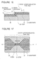
- Step type Josephson junction devices were manufactured by using MgO single crystalline substrates, YSZ (yttrium stabilized zirconia) substrates, SrTiO 3 single crystalline substrates, NdGaO 3 single crystalline substrates and LaAlO 3 single crystalline substrates having steps formed by the method in accordance with the present invention. Referring Figures 1A to 1E, the process for manufacturing the step type junction devices will be described.
- a Nb layer 3 having a thickness of 100 nanometers was deposited on a substrate 2 by sputtering.
- the Nb layer can be also deposited by vacuum evaporation.
- the exposed portion of the substrate 2 was etched by ion milling using Ar ions so as to form a step 23 having a height of 200 nanometers, as shown in Figure 1C.
- the ion milling was conducted under the following condition: Acceleration voltage 600 V Current 200 mA Pressure 1. 333 x 10 -2 Pa (1 ⁇ 10 -4 Torr) Duration 15 minutes
- the etched surface 22 of the substrate 2 was further etched to a depth of 5 nanometers by low acceleration voltage ion milling using Ar ions in order to remove a degraded surface.
- the conditions of the low acceleration voltage ion milling were as follows: Acceleration voltage 70 - 80 V Current 150 - 250 mA Pressure 1.333 ⁇ 10 -2 -3.999 ⁇ 10 -2 Pa (1 ⁇ 10 -4 - 3 x 10 -4 Torr) Duration 30 minutes
- acceleration voltage is lower than 70 volts, it takes too long time to etch the substrate to an enough depth. If the acceleration voltage is higher than 80 volts, the etched surface is again degraded.
- Nb layer 3 was completely removed by utilizing CF 4 plasma so as to expose non-etched surface 21 of the substrate 2 as shown in figure 1 D.
- a Y 1 Ba 2 Cu 3 O 7-x oxide superconductor thin film 1 having a thickness of 200 nanometers was deposited on the substrate 2 by laser ablation as shown in figure 1E.
- the conditions of the laser ablation process were as follows : Target Y 1 Ba 2 Cu 3 O 7-x pellet (sintered) Temperature of substrate 700°C Atmosphere O 2 Pressure 53,32 Pa (400 mTorr) Laser energy 0.4 Joule/pulse Density of laser energy 2.0 Joule/cm 2 Laser pulse rate 5 Hz
- the Y 1 Ba 2 Cu 3 O 7-x oxide superconductor thin film 1 was patterned by a photolithography process so as to form a bridge portion 10 having a width of 5 ⁇ m and length of 10 ⁇ m between portions 11 and 12, as shown in figure 1F. With this, the step type Josephson junction device was completed.
- step type Josephson junction device Characteristics of the above mentioned step type Josephson junction device was evaluated at the liquid nitrogen temperature, so that 70 to 75 percent of the step type Josephson junction devices manufactured for each of the MgO single crystalline substrate, YSZ substrate, SrTiO 3 single crystalline substrate, NdGaO 3 single crystalline substrate and LaAlO 3 single crystalline substrate by the above process functioned at the liquid nitrogen temperature.
- the surface of the substrate 2 was further etched chemically to a depth of 5 nanometers by wet etching process.
- the chemical etching was conducted by respectively using sulfuric acid, mixture of nitric acid and hydrofluoric acid, and phosphoric acid. The conditions were shown as follows: Acid Temperature Duration Concentrated sulfuric acid Room temperature 2 - 5 min. Mixture of nitric acid and hydrofluoric acid nitric: hydrofluoric: water acid acid 2 : 2 : 1 (by volume) Room temperature 10 - 20 sec. Concentrated phosphoric acid 100 -150 °C 10 - 20 sec.
- a Y 1 Ba 2 Cu 3 O 7-x oxide superconductor thin film 1 having a thickness of 200 nanometers was deposited on the substrate 2 by laser ablation under the same conditions as Embodiment 1.
- the Y 1 Ba 2 Cu 3 O 7-x oxide superconductor thin film 1 was patterned so as to form an equal Josephson junction device to that of Embodiment 1.
- step type Josephson junction devices manufactured by the above process were evaluated at the liquid nitrogen temperature. By this, it became clear that 90 to 92 percent of the step type Josephson junction devices formed on subsrates etched by the concentrated sulfuric acid functioned at the liquid nitrogen temperature. 89 to 92 percent of the step type Josephson junction devices formed on subsrates etched by the mixture of nitric acid and hydrofluoric acid functioned at the liquid nitrogen temperature. 90 to 92 percent of the step type Josephson junction devices formed on subsrates etched by the concentrated phosphoric acid functioned at the liquid nitrogen temperature.
- a third embodiment of the process for manufacturing the step type Josephson junction device will be described.
- this third embodiment only YSZ substrates were used and the same processings as those shown in Figures 1A to 1C were performed.
- the surface of the substrate 2 was further etched chemically to a depth of 5 nanometers by wet etching process.
- the chemical etching was conducted by respectively using hydrofluoric acid and mixture of nitric acid and hydrofluoric acid. The conditions were shown as follows: Acid Temperature Duration Hydrofluoric acid (20 - 50 percent aqueous solution) Room temperature 1 - 3 min. Mixture of nitric acid and hydrofluoric acid nitric: hydrofluoric: water acid acid 4 : 3 : 1 (by volume) Room temperature 20 - 40 sec.
- a Y 1 Ba 2 Cu 3 O 7-x oxide superconductor thin film 1 having a thickness of 200 nanometers was deposited on the substrate 2 by laser ablation under the same conditions as Embodiment 1.
- the Y 1 Ba 2 Cu 3 O 7-x oxide superconductor thin film 1 was patterned so as to form an equal Josephson junction device to that of Embodiment 1.
- the surface of the substrate 2 was further etched chemically to a depth of 5 nanometers by wet etching process.
- the chemical etching was conducted by respectively using hydrofluoric acid, mixture of nitric acid and hydrofluoric acid, phosphoric acid and solution of sodium hydroxide. The conditions were shown as follows: Medium Temperature Duration Hydrofluoric acid (10 - 30 percent aqueous solution) Room temperature 5 - 10 min.
- nitric acid and hydrofluoric acid nitric hydrofluoric: water acid acid 3 : 3 : 1 (by volume) Room temperature 30 sec. - 2 min. Concentrated phosphoric acid 100 -150 °C 10 - 30 sec. Concentrated solution of sodium hydroxide 80 -130 °C 3 - 5 min.
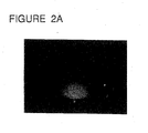
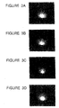
- RHEED Surface crystallinity of the etched substrates was evaluated by RHEED before and after the above chemical etching.
- the RHEED images had been halo patterns before the chemical etching and became streak patterns after the chemical etching, so that it became clear that crystallinity was recovered at the etched portions and they had a good surface condition.
- RHEED images of the substrates after the chemical etching in Figures 3A to 3D.
- a Y 1 Ba 2 Cu 3 O 7-x oxide superconductor thin film 1 having a thickness of 200 nanometers was deposited on the substrate 2 by laser ablation under the same conditions as Embodiment 1.
- the Y 1 Ba 2 Cu 3 O 7-x oxide superconductor thin film 1 was patterned so as to form an equal Josephson junction device to that of Embodiment 1.
- a fifth embodiment of the process for manufacturing the step type Josephson junction device will be described.
- this fifth embodiment only NdGaO 3 substrates were used and the same processings as those shown in Figures 1A to 1C were performed.
- the surface of the substrate 2 was further etched chemically to a depth of 5 nanometers by wet etching process.
- the chemical etching was conducted by respectively using mixture of nitric acid and hydrofluoric acid, and solution of sodium hydroxide. The conditions were shown as follows: Medium Temperature Duration Mixture of nitric acid and hydrofluoric acid nitric: hydrofluoric: water acid acid 2 : 2 : 1 (by volume) Room temperature 10 - 20 sec. Concentrated solution of sodium hydroxide 80 -130 °C 3 - 5 min.
- a Y 1 Ba 2 Cu 3 O 7-x oxide superconductor thin film 1 having a thickness of 200 nanometers was deposited on the substrate 2 by laser ablation under the same conditions as Embodiment 1.
- the Y 1 Ba 2 Cu 3 O 7-x oxide superconductor thin film 1 was patterned so as to form an equal Josephson junction device to that of Embodiment 1.
- a sixth embodiment of the process for manufacturing the step type Josephson junction device will be described.
- only LaAlO 3 substrates were used and the same processings as those shown in Figures 1A to 1C were performed.
- the surface of the substrate 2 was further etched chemically to a depth of 5 nanometers by wet etching process.
- the chemical etching was conducted by respectively using mixture of nitric acid and hydrofluoric acid, phosphoric acid and solution of sodium hydroxide. The conditions were shown as follows: Medium Temperature Duration Mixture of nitric acid and hydrofluoric acid nitric: hydrofluoric: water acid acid 2 : 2 : 1 (by volume) Room temperature 1 - 3 sec. Concentrated phosphoric acid 70 -110 °C 10 - 30 sec. Concentrated solution of sodium hydroxide 50 -110 °C 1 - 3 min.
- a Y 1 Ba 2 Cu 3 O 7-x oxide superconductor thin film 1 having a thickness of 200 nanometers was deposited on the substrate 2 by laser ablation under the same conditions as Embodiment 1.
- the Y 1 Ba 2 Cu 3 O 7-x oxide superconductor thin film 1 was patterned so as to form an equal Josephson junction device to that of Embodiment 1.
- a step on a substrate without degrading crystallinity of the surface of the substrate.
- a high quality oxide superconductor thin film can be deposited on the surface of the substrate processed in accordance with the method of the present invention, so that superconducting devices such as step type Josephson junction devices can be easily manufactured.
- the substrates were etched by ion milling using Ar ions in order to form a step.
- the present invention can be applied to any etching process, if the etched surface of the substrate is lost its crystallinity, for example reactive ion etching, sputtering etching, etc.
- the oxide superconductor thin film can be formed of not only the Y-Ba-Cu-O compound oxide superconductor material, but also a high-T c (high critical temperature) oxide superconductor material, particularly a high-T c copper-oxide type compound oxide superconductor material, for example a Bi-Sr-Ca-Cu-O compound oxide superconductor material, and a Tl-Ba-Ca-Cu-O compound oxide superconductor material.
- a high-T c oxide superconductor material particularly a high-T c copper-oxide type compound oxide superconductor material, for example a Bi-Sr-Ca-Cu-O compound oxide superconductor material, and a Tl-Ba-Ca-Cu-O compound oxide superconductor material.
Landscapes
- Engineering & Computer Science (AREA)
- Chemical & Material Sciences (AREA)
- Ceramic Engineering (AREA)
- Manufacturing & Machinery (AREA)
- Superconductor Devices And Manufacturing Methods Thereof (AREA)
- Superconductors And Manufacturing Methods Therefor (AREA)
Claims (17)
- Procédé pour former une partie étagée sur une surface de dépôt d'un substrat-formé d'oxyde pour un dispositif de type étagé à oxyde supraconducteur, pour le dépôt d'un film mince sur ce substrat, comprenant les étapes consistant à soumettre à une attaque à sec une partie de la surface de dépôt du substrat et en outre continuer à appliquer une attaque légère uniquement à la partie attaquée de la surface du substrat, par fraisage ionique en utilisant des ions Ar avec une tension accélératrice comprise entre 70 et 80 volts, ou appliquer en outre une attaque légère à la surface du substrat par attaque chimique de manière à éliminer une surface altérée afin d'exposer une surface présentant une cristallinité élevée.
- Procédé selon la revendication 1, selon lequel l'attaque chimique est exécutée moyennant l'utilisation d'un agent d'attaque choisi dans le groupe comprenant l'acide sulfurique, l'acide fluorhydrique, l'acide phosphorique, une solution d'hydroxyde de sodium et un mélange d'acide nitrique et d'acide chlorhydrique.
- Procédé selon la revendication 2, selon lequel l'attaque chimique est exécutée en utilisant de l'acide sulfurique à la température ambiante.
- Procédé selon la revendication 3, selon lequel le substrat est un substrat en MgO monocristallin et l'attaque chimique est exécutée en utilisant de l'acide sulfurique concentré.
- Procédé selon la revendication 2, selon lequel l'attaque chimique est exécutée en utilisant de l'acide fluorhydrique à la température ambiante.
- Procédé selon la revendication 5, selon lequel le substrat est un substrat en YSZ et l'attaque chimique est exécutée en utilisant une solution aqueuse à 20-50 pour cent d'acide fluorhydrique.
- Procédé selon la revendication 5, selon lequel le substrat est un substrat en SrTiO3 et l'attaque chimique est exécutée en utilisant une solution aqueuse à 10-30 pour cent d'acide chlorhydrique.
- Procédé selon la revendication 2, selon lequel l'attaque chimique est exécutée en utilisant de l'acide. phosphorique à une température comprise entre 100 et 150°C.
- Procédé selon la revendication 8, selon lequel le substrat est choisi dans le groupe comprenant un substrat en MgO monocristallin, un substrat en SrTiO3 monocristallin et un substrat en LaAlO3 monocristallin, et l'attaque chimique est exécutée en utilisant de l'acide phosphorique concentré.
- Procédé selon la revendication 2, selon lequel l'attaque chimique est exécutée en utilisant une solution d'hydroxyde de sodium à une température comprise entre 50 et 130°C.
- Procédé selon la revendication 10, selon lequel le substrat est un substrat de SrToO3 monocristallin ou un substrat de NdGaO3 monocristallin, et l'attaque chimique est exécutée en utilisant une solution concentrée d'hydroxyde de sodium à une température comprise entre 80 et 130°C.
- Procédé selon la revendication 10, selon lequel le substrat est un substrat en LaAlO3 monocristallin et l'attaque chimique est exécutée en utilisant une solution concentrique d'hydroxyde de sodium à une température comprise entre 50 et 110°C.
- Procédé selon la revendication 2, selon lequel l'attaque chimique est exécutée en utilisant un mélange d'acide nitrique et d'acide fluorhydrique à la température ambiante.
- Procédé selon la revendication 13, selon lequel le substrat est un substrat en MgO monocristallin ou un substrat en NdGaO3, et l'attaque chimique est exécutée en utilisant un mélange d'acide nitrique et d'acide fluorhydrique incluant 2 parties d'acide nitrique, 2 parties d'acide fluorhydrique et 1 partie d'eau en volume.
- Procédé selon la revendication 13, selon lequel le substrat est un substrat en YSZ et l'attaque chimique est effectuée en utilisant un mélange d'acide nitrique et d'acide fluorhydrique incluant 4 parties d'acide nitrique, 3 parties d'acide fluorhydrique et 1 partie d'eau en volume.
- Procédé selon la revendication 13, selon lequel le substrat est un substrat en SrTiO3 ou un substrat en LaAlO3 et l'attaque chimique est exécutée en utilisant un mélange d'acide nitrique et d'acide fluorhydrique et 1 partie d'eau en volume.
- Procédé pour fabriquer un dispositif à jonction de Josephson de type étagé, comprenant une étape consistant à former un film mince d'oxyde supraconducteur sur une surface de dépôt d'un substrat, comprenant une partie étagée formée par un procédé selon l'une quelconque des revendications 1 à 16.
Applications Claiming Priority (3)
| Application Number | Priority Date | Filing Date | Title |
|---|---|---|---|
| JP5348838A JPH0779021A (ja) | 1993-07-15 | 1993-12-27 | 成膜用基板に段差を形成する方法 |
| JP34883893 | 1993-12-27 | ||
| JP348838/93 | 1993-12-27 |
Publications (3)
| Publication Number | Publication Date |
|---|---|
| EP0660428A2 EP0660428A2 (fr) | 1995-06-28 |
| EP0660428A3 EP0660428A3 (fr) | 1997-07-16 |
| EP0660428B1 true EP0660428B1 (fr) | 2001-09-05 |
Family
ID=18399727
Family Applications (1)
| Application Number | Title | Priority Date | Filing Date |
|---|---|---|---|
| EP94402527A Expired - Lifetime EP0660428B1 (fr) | 1993-12-27 | 1994-11-08 | Procédé de fabrication d'une marche sur la surface de dépôt d'un substrat pour un dispositif supraconducteur comportant un supraconducteur d'oxyde |
Country Status (7)
| Country | Link |
|---|---|
| US (1) | US5560836A (fr) |
| EP (1) | EP0660428B1 (fr) |
| KR (1) | KR100297531B1 (fr) |
| CA (1) | CA2135500C (fr) |
| DE (1) | DE69428182T2 (fr) |
| DK (1) | DK0660428T3 (fr) |
| FI (1) | FI111198B (fr) |
Families Citing this family (11)
| Publication number | Priority date | Publication date | Assignee | Title |
|---|---|---|---|---|
| WO1998050965A1 (fr) * | 1997-05-02 | 1998-11-12 | Superconductor Technologies, Inc. | Procede de preparation de substrats pour supraconducteurs a couche mince et dispositifs perfectionnes renfermant ces substrats |
| DE19808778C2 (de) * | 1998-03-03 | 1999-12-09 | Forschungszentrum Juelich Gmbh | Verfahren zur Herstellung eines ABO¶3¶-Substrates mit einer Stufe |
| AUPP590798A0 (en) | 1998-09-14 | 1998-10-08 | Commonwealth Scientific And Industrial Research Organisation | Method of manufacture of high temperature superconductors |
| US6734699B1 (en) | 1999-07-14 | 2004-05-11 | Northrop Grumman Corporation | Self-clocked complementary logic |
| US7015499B1 (en) | 1999-12-01 | 2006-03-21 | D-Wave Systems, Inc. | Permanent readout superconducting qubit |
| US6459097B1 (en) | 2000-01-07 | 2002-10-01 | D-Wave Systems Inc. | Qubit using a Josephson junction between s-wave and d-wave superconductors |
| US6627915B1 (en) | 2000-08-11 | 2003-09-30 | D-Wave Systems, Inc. | Shaped Josephson junction qubits |
| US6504172B2 (en) | 2001-03-16 | 2003-01-07 | D-Wave Systems, Inc. | Superconducting dot/anti-dot flux qubit based on time-reversal symmetry breaking effects |
| US7002366B2 (en) * | 2003-08-20 | 2006-02-21 | Northrop Grumman Corporation | Superconducting constant current source |
| US20050062131A1 (en) * | 2003-09-24 | 2005-03-24 | Murduck James Matthew | A1/A1Ox/A1 resistor process for integrated circuits |
| ATE441378T1 (de) * | 2007-04-19 | 2009-09-15 | Straumann Holding Ag | Verfahren zur bereitstellung einer topographie auf der oberfläche eines zahnimplantats |
Citations (3)
| Publication number | Priority date | Publication date | Assignee | Title |
|---|---|---|---|---|
| EP0293134A1 (fr) * | 1987-05-25 | 1988-11-30 | Matsushita Electronics Corporation | Procédé pour la fabrication de capacités en creusant des cellules sur un substrat à semi-conducteur |
| EP0655789A1 (fr) * | 1993-11-29 | 1995-05-31 | SAMSUNG ELECTRO-MECHANICS Co. Ltd. | Procédé de fabrication de dispositifs Josephson supraconducteurs à haute température |
| US5780343A (en) * | 1995-12-20 | 1998-07-14 | National Semiconductor Corporation | Method of producing high quality silicon surface for selective epitaxial growth of silicon |
Family Cites Families (4)
| Publication number | Priority date | Publication date | Assignee | Title |
|---|---|---|---|---|
| US5077266A (en) * | 1988-09-14 | 1991-12-31 | Hitachi, Ltd. | Method of forming weak-link josephson junction, and superconducting device employing the junction |
| JPH05251771A (ja) * | 1991-12-02 | 1993-09-28 | Sumitomo Electric Ind Ltd | 人工粒界型ジョセフソン接合素子およびその作製方法 |
| JP2730368B2 (ja) * | 1991-12-10 | 1998-03-25 | 住友電気工業株式会社 | 超電導電界効果型素子およびその作製方法 |
| JPH05335638A (ja) * | 1992-05-29 | 1993-12-17 | Sumitomo Electric Ind Ltd | ジョセフソン接合構造体およびその作製方法 |
-
1994
- 1994-11-07 FI FI945234A patent/FI111198B/fi not_active IP Right Cessation
- 1994-11-08 DK DK94402527T patent/DK0660428T3/da active
- 1994-11-08 DE DE69428182T patent/DE69428182T2/de not_active Expired - Fee Related
- 1994-11-08 EP EP94402527A patent/EP0660428B1/fr not_active Expired - Lifetime
- 1994-11-09 CA CA002135500A patent/CA2135500C/fr not_active Expired - Fee Related
- 1994-11-09 US US08/338,094 patent/US5560836A/en not_active Expired - Fee Related
- 1994-11-18 KR KR1019940030354A patent/KR100297531B1/ko not_active Expired - Fee Related
Patent Citations (3)
| Publication number | Priority date | Publication date | Assignee | Title |
|---|---|---|---|---|
| EP0293134A1 (fr) * | 1987-05-25 | 1988-11-30 | Matsushita Electronics Corporation | Procédé pour la fabrication de capacités en creusant des cellules sur un substrat à semi-conducteur |
| EP0655789A1 (fr) * | 1993-11-29 | 1995-05-31 | SAMSUNG ELECTRO-MECHANICS Co. Ltd. | Procédé de fabrication de dispositifs Josephson supraconducteurs à haute température |
| US5780343A (en) * | 1995-12-20 | 1998-07-14 | National Semiconductor Corporation | Method of producing high quality silicon surface for selective epitaxial growth of silicon |
Also Published As
| Publication number | Publication date |
|---|---|
| CA2135500C (fr) | 2000-05-02 |
| KR100297531B1 (ko) | 2001-10-24 |
| DE69428182D1 (de) | 2001-10-11 |
| FI945234L (fi) | 1995-06-28 |
| EP0660428A3 (fr) | 1997-07-16 |
| FI111198B (fi) | 2003-06-13 |
| EP0660428A2 (fr) | 1995-06-28 |
| DE69428182T2 (de) | 2002-03-28 |
| DK0660428T3 (da) | 2001-12-27 |
| US5560836A (en) | 1996-10-01 |
| CA2135500A1 (fr) | 1995-06-28 |
| FI945234A0 (fi) | 1994-11-07 |
Similar Documents
| Publication | Publication Date | Title |
|---|---|---|
| EP0480814B1 (fr) | Dispositif supraconducteur avec un canal ultra-mince forme en matériau supraconducteur d'oxyde et procédé pour sa fabrication | |
| US5750474A (en) | Method for manufacturing a superconductor-insulator-superconductor Josephson tunnel junction | |
| EP0660428B1 (fr) | Procédé de fabrication d'une marche sur la surface de dépôt d'un substrat pour un dispositif supraconducteur comportant un supraconducteur d'oxyde | |
| US5439875A (en) | Process for preparing Josephson junction device having weak link of artificial grain boundary | |
| EP0421889B1 (fr) | Méthode pour former une couche de supraconducteur d'oxyde continue avec des régions différentes pour dispositifs supraconducteurs | |
| US5382566A (en) | Josephson junction device formed of oxide superconductor and process for preparing the same | |
| US5446016A (en) | Method for forming a patterned oxide superconductor thin film | |
| EP0502787B1 (fr) | Couche mince d'un matériau supraconducteur d'oxide avec localement différentes orientations cristallines et un procédé pour sa préparation | |
| EP0546904B1 (fr) | Méthode pour fabriquer un dispositif à jonction artificielle de type Josephson à limite de grain | |
| US5422337A (en) | Step-edged grain boundary Josephson junction with 5 to 30 degrees inclined angle | |
| US5408108A (en) | Superconducting device having an extremely thin superconducting channel formed of oxide superconductor material | |
| EP0551033B1 (fr) | Dispositif supraconducteur à canal supraconducteur extrêmement mince en oxyde supraconducteur et procédé pour sa fabrication | |
| EP0484232B2 (fr) | Dispositif supraconducteur ayant un canal supraconducteur extrêmement court en matériau supraconducteur d'oxyde et méthode pour sa fabrication | |
| EP0508844B1 (fr) | Couche mince supraconductrice ayant au moins une région isolée supraconductrice formée en matériau supraconducteur d'oxyde et méthode pour sa fabrication | |
| US5612290A (en) | Josephson junction device formed of oxide superconductor | |
| EP0533519B1 (fr) | Dispositif supraconducteur ayant un canal extrêmement mince, formé en matériau supraconducteur d'oxyde et méthode pour sa fabrication | |
| US5721196A (en) | Stacked tunneling and stepped grain boundary Josephson junction | |
| EP0506573B1 (fr) | Procédé pour nettoyer la surface d'une couche mince d'oxyde supraconducteur | |
| EP0524862B1 (fr) | Dispositif à jonction Josephson en oxyde supraconducteur et procédé pour sa fabrication | |
| EP0545815B1 (fr) | Dispositif à jonction Josephson en oxyde supraconducteur et procédé pour sa fabrication | |
| EP0557207A1 (fr) | Dispositif à jonction de type Josephson à supraconducteur d'oxyde et procédé de préparation |
Legal Events
| Date | Code | Title | Description |
|---|---|---|---|
| PUAI | Public reference made under article 153(3) epc to a published international application that has entered the european phase |
Free format text: ORIGINAL CODE: 0009012 |
|
| AK | Designated contracting states |
Kind code of ref document: A2 Designated state(s): DE DK FR GB IT NL |
|
| PUAL | Search report despatched |
Free format text: ORIGINAL CODE: 0009013 |
|
| AK | Designated contracting states |
Kind code of ref document: A3 Designated state(s): DE DK FR GB IT NL |
|
| 17P | Request for examination filed |
Effective date: 19970628 |
|
| 17Q | First examination report despatched |
Effective date: 19971107 |
|
| GRAG | Despatch of communication of intention to grant |
Free format text: ORIGINAL CODE: EPIDOS AGRA |
|
| GRAG | Despatch of communication of intention to grant |
Free format text: ORIGINAL CODE: EPIDOS AGRA |
|
| GRAH | Despatch of communication of intention to grant a patent |
Free format text: ORIGINAL CODE: EPIDOS IGRA |
|
| GRAH | Despatch of communication of intention to grant a patent |
Free format text: ORIGINAL CODE: EPIDOS IGRA |
|
| GRAA | (expected) grant |
Free format text: ORIGINAL CODE: 0009210 |
|
| AK | Designated contracting states |
Kind code of ref document: B1 Designated state(s): DE DK FR GB IT NL |
|
| ITF | It: translation for a ep patent filed | ||
| REF | Corresponds to: |
Ref document number: 69428182 Country of ref document: DE Date of ref document: 20011011 |
|
| ET | Fr: translation filed | ||
| REG | Reference to a national code |
Ref country code: GB Ref legal event code: IF02 |
|
| PLBE | No opposition filed within time limit |
Free format text: ORIGINAL CODE: 0009261 |
|
| STAA | Information on the status of an ep patent application or granted ep patent |
Free format text: STATUS: NO OPPOSITION FILED WITHIN TIME LIMIT |
|
| 26N | No opposition filed | ||
| PGFP | Annual fee paid to national office [announced via postgrant information from national office to epo] |
Ref country code: GB Payment date: 20021106 Year of fee payment: 9 |
|
| PGFP | Annual fee paid to national office [announced via postgrant information from national office to epo] |
Ref country code: FR Payment date: 20021108 Year of fee payment: 9 |
|
| PGFP | Annual fee paid to national office [announced via postgrant information from national office to epo] |
Ref country code: DK Payment date: 20021113 Year of fee payment: 9 |
|
| PGFP | Annual fee paid to national office [announced via postgrant information from national office to epo] |
Ref country code: DE Payment date: 20021114 Year of fee payment: 9 |
|
| PGFP | Annual fee paid to national office [announced via postgrant information from national office to epo] |
Ref country code: NL Payment date: 20021129 Year of fee payment: 9 |
|
| PG25 | Lapsed in a contracting state [announced via postgrant information from national office to epo] |
Ref country code: GB Free format text: LAPSE BECAUSE OF NON-PAYMENT OF DUE FEES Effective date: 20031108 |
|
| PG25 | Lapsed in a contracting state [announced via postgrant information from national office to epo] |
Ref country code: DK Free format text: LAPSE BECAUSE OF NON-PAYMENT OF DUE FEES Effective date: 20031201 |
|
| PG25 | Lapsed in a contracting state [announced via postgrant information from national office to epo] |
Ref country code: NL Free format text: LAPSE BECAUSE OF NON-PAYMENT OF DUE FEES Effective date: 20040601 |
|
| PG25 | Lapsed in a contracting state [announced via postgrant information from national office to epo] |
Ref country code: DE Free format text: LAPSE BECAUSE OF NON-PAYMENT OF DUE FEES Effective date: 20040602 |
|
| GBPC | Gb: european patent ceased through non-payment of renewal fee |
Effective date: 20031108 |
|
| REG | Reference to a national code |
Ref country code: DK Ref legal event code: EBP |
|
| PG25 | Lapsed in a contracting state [announced via postgrant information from national office to epo] |
Ref country code: FR Free format text: LAPSE BECAUSE OF NON-PAYMENT OF DUE FEES Effective date: 20040730 |
|
| NLV4 | Nl: lapsed or anulled due to non-payment of the annual fee |
Effective date: 20040601 |
|
| REG | Reference to a national code |
Ref country code: FR Ref legal event code: ST |
|
| PG25 | Lapsed in a contracting state [announced via postgrant information from national office to epo] |
Ref country code: IT Free format text: LAPSE BECAUSE OF NON-PAYMENT OF DUE FEES;WARNING: LAPSES OF ITALIAN PATENTS WITH EFFECTIVE DATE BEFORE 2007 MAY HAVE OCCURRED AT ANY TIME BEFORE 2007. THE CORRECT EFFECTIVE DATE MAY BE DIFFERENT FROM THE ONE RECORDED. Effective date: 20051108 |