EP0660989B1 - Dispositif de commande de polarisation pour un extracteur de donnees dans un decodeur auxiliaire d'informations video - Google Patents
Dispositif de commande de polarisation pour un extracteur de donnees dans un decodeur auxiliaire d'informations video Download PDFInfo
- Publication number
- EP0660989B1 EP0660989B1 EP93918512A EP93918512A EP0660989B1 EP 0660989 B1 EP0660989 B1 EP 0660989B1 EP 93918512 A EP93918512 A EP 93918512A EP 93918512 A EP93918512 A EP 93918512A EP 0660989 B1 EP0660989 B1 EP 0660989B1
- Authority
- EP
- European Patent Office
- Prior art keywords
- signal
- count
- video
- value
- ric
- Prior art date
- Legal status (The legal status is an assumption and is not a legal conclusion. Google has not performed a legal analysis and makes no representation as to the accuracy of the status listed.)
- Expired - Lifetime
Links
Images




Classifications
-
- H—ELECTRICITY
- H04—ELECTRIC COMMUNICATION TECHNIQUE
- H04N—PICTORIAL COMMUNICATION, e.g. TELEVISION
- H04N7/00—Television systems
- H04N7/08—Systems for the simultaneous or sequential transmission of more than one television signal, e.g. additional information signals, the signals occupying wholly or partially the same frequency band, e.g. by time division
- H04N7/087—Systems for the simultaneous or sequential transmission of more than one television signal, e.g. additional information signals, the signals occupying wholly or partially the same frequency band, e.g. by time division with signal insertion during the vertical blanking interval only
-
- H—ELECTRICITY
- H04—ELECTRIC COMMUNICATION TECHNIQUE
- H04N—PICTORIAL COMMUNICATION, e.g. TELEVISION
- H04N7/00—Television systems
- H04N7/025—Systems for the transmission of digital non-picture data, e.g. of text during the active part of a television frame
- H04N7/035—Circuits for the digital non-picture data signal, e.g. for slicing of the data signal, for regeneration of the data-clock signal, for error detection or correction of the data signal
- H04N7/0355—Circuits for the digital non-picture data signal, e.g. for slicing of the data signal, for regeneration of the data-clock signal, for error detection or correction of the data signal for discrimination of the binary level of the digital data, e.g. amplitude slicers
-
- H—ELECTRICITY
- H04—ELECTRIC COMMUNICATION TECHNIQUE
- H04N—PICTORIAL COMMUNICATION, e.g. TELEVISION
- H04N5/00—Details of television systems
- H04N5/14—Picture signal circuitry for video frequency region
- H04N5/16—Circuitry for reinsertion of DC and slowly varying components of signal; Circuitry for preservation of black or white level
- H04N5/18—Circuitry for reinsertion of DC and slowly varying components of signal; Circuitry for preservation of black or white level by means of "clamp" circuit operated by switching circuit
Definitions
- the present invention relates to detection of information that may be present in a video signal during vertical blanking intervals.
- a video signal typically includes vertical display intervals, or fields, having a plurality of horizontal line intervals, e.g. 262.5 lines per field in NTSC video systems. The beginning of each vertical and horizontal interval is identified by respective vertical and horizontal sync pulses that are included in a composite video signal. During a portion of each vertical interval, information in the video signal may not be intended for display. For example, a vertical blanking interval spans approximately the first 20 horizontal line intervals in each field. In addition, several line intervals adjacent to the vertical blanking period, e.g. line 21, may be within an overscan region of a video display and will not be visible.
- auxiliary information component e.g. teletext or closed caption data
- Standards such as Federal Communications Commissions (FCC) Regulations define the format for each type of auxiliary information including the positioning of the information within a vertical interval.
- FCC Federal Communications Commissions
- the present closed captioning standard (see e.g. 47 CFR ⁇ 15.119 and 73.682) specifies that digital data corresponding to ASCII characters for closed captioning must be in line 21 of field 1. Future modifications to the standard may permit auxiliary information such as closed caption data to be located in other lines, e.g. line 21 of every field.
- Auxiliary video information is extracted from the video signal using a decoder.
- An important part of a decoder is the data slicer.
- the data slicer may be a voltage comparator having a video signal carrying auxiliary video information applied to one input.
- a reference or "slicing" voltage at a second input of the comparator should be at the midpoint of the peak to peak excursion of the auxiliary video information signal.
- the output of the comparator would then provide a binary signal representative of the auxiliary information contained in the video signal.
- a constant slicing level may not be adequate for all video signals.
- Video signal levels may vary depending on the source of the video signal. Utilizing a constant slicing level with varying video signal levels may bias the extracted data undesirably toward logic 0 or logic 1 resulting in erroneous data extraction. For example, if the video signal range is 0 IRE to 20 IRE, a slicing level of 10 IRE is desirable while for a video signal range of 0 IRE to 50 IRE, a slicing level of 25 IRE is desirable. If 25 IRE were used as a slicing level for a signal range of 0 IRE to 20 IRE, a logic 1 would never be extracted because the signal never exceeds the slicing level. Thus, it is desirable to adapt the slicing level to the amplitude of the input video signal.
- auxiliary information component such as closed caption data includes provisions to facilitate an adaptive slicing level function.
- a closed caption signal in line 21 begins after the "back porch" interval of the video signal with a 7 cycle burst of a sinusoidal reference waveform designated the "run-in clock" (RIC).
- the RIC reference component of the auxiliary video data signal is followed in the latter half of the line 21 interval by a data signal component that represents the actual closed caption data.
- the closed caption data standard establishes that the amplitude of the RIC signal is identical to the amplitude of the data signal. Thus, the average of the RIC signal amplitude is an appropriate slicing level for the subsequent data signal.
- One method for developing the slicing voltage is to integrate the sinusoidal RIC signal and use the resulting DC voltage as the bias for the data slicer.
- a large integrator capacitor may be required to prevent the slicing voltage from changing due to leakage currents discharging the capacitor during the interval between occurrences of auxiliary video data (e.g. the interval from one line 21 to the next for closed caption data).
- a large capacitor requires long integration intervals to respond to changes in video signal levels when changing the slicing level. For example, in a closed caption signal, the RIC signal is present only for 14 ⁇ s (7 cycles of 500KHz sinewave) at 33.3 ms intervals (period of one frame of video).
- a large capacitor may require a response time on the order of one second to respond to sudden changes in the signal level. A significant amount of auxiliary video information during the response interval may be undetected.
- auxiliary video information decoder in a video signal processing integrated circuit (IC).
- IC video signal processing integrated circuit
- a large integrating capacitor may, however, be too large to be included in the IC.
- An extra IC pin would be required for connecting an external integrating capacitor.
- IC parameters may vary during production.
- a design having tight tolerances may be incompatible (produce unexpected or undesirable performance) as a result of parameter variations during IC production.
- the present invention resides, in part, in recognition of the described problems and, in part, in providing an auxiliary video information decoder that solves the problem.
- an apparatus is provided as specified in claim 1.
- coupling capacitor CIN couples input video signal VIDEO to black level clamp 210.
- a typical value for capacitor CIN is 1 ⁇ F.
- Black level clamp 210 is enabled to clamp the level of signal VIN to a level related to desired black level reference level VREF during intervals determined by control signal TGC from control ⁇ C 200, e.g Motorola MC68HC05. The operation of black level clamp 210 is described further below.
- Signal VIN at the output of black level clamp 210 is coupled to data slicer 230 and sync separator 240 which produce output signals SLICED DATA and SEP SYNC, respectively, by comparing signal VIN to respective reference voltage levels VS and V0.
- Signal SLICED DATA is a binary representation of the information in signal VIN.
- Signal SEP SYNC is a synchronizing waveform having pulses corresponding to the synchronizing pulses in signal VIN. Because signal SEP SYNC is derived from the actual video signal, the sync pulses in signal SEP SYNC provide an accurate indication of when intervals of interest in the video signal, e.g. line 21, actually occur.
- Signal SEP SYNC may be used by circuits not shown in Figure 2 that capture the binary auxiliary video information on signal SLICED DATA. For example, signal SEP SYNC may be used to generate an enable signal to enable data capture circuitry when binary values representative of auxiliary video information are occurring on signal SLICED DATA. As an example, the derived enable signal might enable a shift register to begin shifting in (capturing) data values on signal SLICED DATA.
- Reference levels VREF, VS, and V0 are generated by reference source 220.
- Signal VR from control ⁇ C 200 is an input to reference source 220 that controls the value of reference level VS.
- the capability to vary reference level VS permits adapting the slicing level to the amplitude characteristics of video signal VIDEO.
- adapting the slicing level also involves counter 250.
- Counter 250 is enabled to count pulses that occur on signal SLICED DATA during intervals defined by one or more control signals from control ⁇ C 200 that are labeled COUNTER CONTROL in Figure 2.
- the counting intervals are established by control ⁇ C 200 to coincide with the intervals when the reference component (e.g. run-in clock or RIC) of an auxiliary video information signal is expected to occur.
- the count value is tested after the RIC interval ends.
- a count value equal to an expected value indicates that the expected number of RIC pulses have been detected demonstrating that the present slicing level is appropriate for extracting auxiliary video information. If the count value does not equal the expected value, the slicing level is adjusted by modifying the value of signal VS.
- control ⁇ C 200 monitors signal SYNC to determine when line 21 of field 1 occurs by counting line synchronizing pulses on signal sync. After a delay (e.g. either a software delay routine or a hardware delay) from the beginning of line 21, control ⁇ C 200 enables counter 250. The delay value is selected to be within the RIC interval. Counting is then enabled for a period that approximately spans an integral number of cycles of the RIC signal. If the slicing level is properly adjusted, the count value should equal the number of peaks of the RIC waveform that occur during the counting interval.
- a delay e.g. either a software delay routine or a hardware delay
- a delay value of 12 ⁇ s and a counting interval of 8 ⁇ s should produce a count of 4 if the slicing level is adjusted properly (four cycles of the 500 kHz RIC waveform occur during an 8 ⁇ s counting interval).
- Figure 3 shows an exemplary embodiment of black level clamp 210, reference source 220, data slicer 230, and sync separator 240 in Figure 2.
- Figure 4 shows an exemplary embodiment of run-in-clock (RIC) counter 250 in Figure 2.
- RIC run-in-clock
- black level clamp 210 includes transmission gate (TG) 302, NOR gate 304, comparator 306, and resistors R1 and R2.
- Reference source 220 includes 4-to-1 MUX 360 and resistors R3 through R9.
- Comparators 230 and 240 are embodiments of data slicer 230 and sync separator 240, respectively.
- the output of NOR gate 304 controls TG 302 such that TG 302 conducts coupling source VCC to resistor R1 when the output of NOR gate 304 is at logic 1.
- a logic 0 level at the output of NOR gate 304 causes TG 302 to become non-conductive decoupling source VCC from resistor R1.
- TG 302 is produced using MOSFET transistors.
- MOSFET transistors As a result, when TG 302 is conductive, it exhibits a characteristic resistance associated with the source-to-drain path through the MOSFET transistors. The value of the resistance depends on design parameters (e.g. transistor width) of the MOSFET transistors.
- NOR gate 304 produces a logic 1 output causing TG 302 to conduct as long as control signal TGC from control ⁇ C 200 is at logic 0 and the output of comparator 306 is at logic 0.
- Comparator 306 compares the value of signal VIN to reference level VREF. Values of signal VIN that exceed reference level VREF cause the output of comparator 306 to go to logic 1, thereby causing TG 302 to be nonconductive.
- TG 302 and resistor R1 exhibit a predetermined resistance ratio with respect to resistor R2 of 11:100 as shown in Figure 3.
- the junction of resistors R1 and R2 is coupled to signal VIN creating a feedback loop.
- the feedback loop and the resistor ratio operate in response to the video signal levels during the sync and blanking intervals in a horizontal line period to charge and discharge node VIN, thereby establishing the desired black level on signal VIN. More specifically, when TG 302 is disabled (non-conductive), the DC level at node VIN discharges via resistor R2. When TG 302 is enabled (conductive), node VIN charges via TG 302 and resistor R1 while discharging via resistor R2. The resistor ratio established by TG 302 and resistors R1 and R2 produces a charge rate that exceeds the discharge rate resulting in a net charging current to node VIN.
- black level clamp 210 To better understand the operation of black level clamp 210, assume that node VIN is initially discharged to 0 volts. In this condition, the level of signal VIN during both sync and blanking intervals of a video line will be less than reference level VREF. Thus, a logic 0 is produced at the output of comparator 306, enabling TG 302 and causing node VIN to charge during both the sync and blanking periods. After a plurality of line intervals, the net charging current will have increased the DC level on node VIN until the level at node VIN exceeds reference level VREF during the blanking interval and is less than reference level VREF during the sync interval.
- the output of comparator 306 will be at logic 1 which disables TG 302 and causes node VIN to discharge.
- the level at node VIN during the sync interval is less than level VREF causing node VIN to charge.
- the resistance values of the charge path (resistance of TG 302 plus resistor R1) and the discharge path (resistor R2) are selected such that discharge during the sync interval equals charge during the blanking period when the DC level at node VIN is approximately equal to level VREF.
- the resulting equilibrium condition clamps the DC level at node VIN to level VREF.
- the described operation is based on a resistance ratio between the discharge-path and the charge-path that is determined for the sync and blanking intervals associated with a particular video signal specification.
- the resistance ratio of 100R (discharge) to 11R (charge) that is shown in Figure 3 is suitable for NTSC standard signals. Other signal standards would require different ratios.
- clamp 210 establishes a desired black level based on sync and blanking intervals having specific durations during each line interval.
- the sync and blanking intervals do not have fixed durations (e.g. wide vertical pulses and narrow equalizing pulses). If clamp 210 operated during the vertical interval, the varying pulse characteristics would cause clamp 210 to undesirably alter the black reference level on node VIN.
- control ⁇ C 200 sets signal TGC to logic 1 during the vertical interval disabling the feedback path of clamp 210 and causing node VIN to discharge relatively slowly via resistor R2 during the vertical interval. When clamp operation resumes following the vertical interval, the desired black level at node VIN is rapidly restored.
- Figure 3 also shows an exemplary embodiment of reference source 220 from Figure 2 that includes resistors R3 through R9 and MUX 360.
- Resistors R3 through R9 are configured as a resistor ladder that provides a plurality of reference levels having values that depend on the ratios of the resistor values. As previously discussed, specifying resistor ratios rather than particular resistor values is desirable for purposes of integrated circuit (IC) implementation.
- Figure 5 shows the relationship between the reference levels generated by the arrangement in Figure 3 and an exemplary video signal waveform that would have a maximum peak-to-peak (100 IRE) amplitude of 1.9 volts.
- the maximum white-going amplitude shown in Figure 5 is 50 IRE which corresponds to the amplitude of an auxiliary information signal as shown in Figure 1.
- Data slicer reference level VS at the output of MUX 360 is coupled to one input of comparator 230 to establish the data slicing level.
- MUX 360 permits the data slicing level to be adapted to the video signal amplitude as desired.
- Reference level VREF for black level clamp 210 is produced at the resistive mid-point (i.e. junction of resistors R7 and R8 or 125R of a total of 250R) of the resistor ladder which is equivalent to 2.5 V for VCC equal to 5 V.
- Sync reference level V0 is produced at the junction of resistors R8 and R9 and is coupled to one input of comparator 240 to establish the sync slicing level.
- sync reference level V0 is approximately equal to -13.5 IRE.
- the indicated value of sync reference level V0 was selected because sync amplitude compression may occur in TV signals. For example, non-standard sync-to-video amplitude ratios may occur in signals extracted from video tapes.
- the selected sync reference level of -13.5 IRE permits comparator 240 to accurately separate sync pulses from a video signal having sync compressed in amplitude to 1/2 of its normal value.
- the voltage selection provided by MUX 360 has been configured to provide a range of slicing levels for data slicer 230 sufficient to adapt the slicing voltage to a variety of video signal variations without requiring a large MUX.
- Limiting the size of MUX 360 is desirable to minimize the number of control signals required and the number of devices required to implement the MUX function. For example, in an integrated circuit (IC) implementation, increasing the size of the MUX requires more transistors and more area on the IC die. In an IC, MUX 360 requires only two control signals and may be implemented using four transmission gates.
- Figure 5 shows the voltages that correspond to the reference levels in Figure 3 with respect to a 1.9 volt peak-to-peak video signal.
- the voltage V2 input to MUX 360 provides a slicing voltage of 2.84 volts as shown in Figure 5 which is approximately equal to the 25 IRE level of a 1.9V peak-to-peak video signal.
- Voltage V3 at 2.98 volts is a desirable slicing level for video signals having a positive offset of 10 IRE. This type of offset may occur in video signals recorded on video tape as part of an approach to preventing unauthorized duplication of prerecorded video programs.
- Two additional bias voltages i.e. voltages V1 and V4, can be selected for optimum data slicing to adapt the slicing level to large deviations of system parameters from their nominal values. Examples of these system parameters are:
- reference source 220 may be adapted to a variety of video signal characteristics and standards.
- run-in-clock (RIC) counter 250 counts pulses of the RIC signal at the output of data slicer 230 (signal SLICED DATA in Figures 2, 3, and 4) to produce count value RIC COUNT that is indicative of when slicing reference level VS is correctly adapted to the video signal.
- An embodiment of counter 250 shown in Figure 4 includes counters 402, 404, and 456, D-type flip-flop (DFF) 452, NAND gates 454 and 458, and inverter 455.
- Count value RIC COUNT is represented by signals RICO and RIC1 that are produced at the two least significant outputs of counter 456 in Figure 4.
- Input signals to Figure 4 include signal 128FH that serves as a clock signal for counter 402.
- Signal 128FH has a frequency that is 128 times horizontal frequency FH or approximately 2 MHz.
- Signal 128 FH may be produced at an output of a counter associated with a phase locked loop (PLL) in the deflection circuitry of a video receiver.
- PLL phase locked loop
- Signal LINE21N is generated by ⁇ C 200 in Figure 2 in response to synchronizing signal SYNC to indicate the occurrence of intervals in the video signal that are expected to include auxiliary video information, e.g. line 21 for closed caption applications.
- Signal LINE21N is used to reset counters 402 and 404, and may be generated by, for example, ⁇ C 200 counting line intervals as indicated by sync pulses in signal SYNC until the desired line number is located.
- Signal LINE21N is at logic 1 to clear (reset) counters 402 and 404 at all times except during the interval when the auxiliary video information signal is expected to occur, e.g. line 21.
- Signal LINE21N then goes to logic 0 to enable counters 402 and 404.
- Signal ENABLE is at logic 1 only during an interval of approximately 25 ⁇ s at the beginning of line 21 to enable DFF 452.
- Signal RICWND at the output of DFF 452 provides an 8 ⁇ s wide window pulse that begins 12 ⁇ s after the beginning of line 21 as shown in Figure 6.
- the window pulse timing is selected to span an 8 ⁇ s portion of the RIC interval during line 21.
- the described timing of signal RICWND is generated as follows.
- Both counter 404 and DFF 452 are clocked by signal CLK which is generated at the most significant output of 4-bit counter 402.
- Signal CLK changes every 8 cycles of the 2 MHz signal 128FH, or every 4 ⁇ s.
- Counters 402 and 404 are clocked by negative-going transitions (logic 1 to logic 0) in signal CLK while DFF 452 is clocked by positive-going transitions (logic 0 to logic 1) in signal CLK.
- the first transition on signal CLK after counters 402 and 404 are enabled is a positive-going transition that occurs 4 ⁇ s after signal LINE21N goes to logic 0.
- this transition clocks DFF 452, counter 404 is cleared (all outputs at logic 0) at this time because no negative-going transitions have occurred on signal CLK.
- a logic 0 is clocked into DFF 452 causing signal RICWND to remain at logic 0.
- a negative-going transition occurs on signal CLK at 8 ⁇ s after signal LINE21N goes to logic 0 causing the least significant output of counter 404 (and the D input to DFF 452) to go to logic 1.
- the next positive-going transition on signal CLK occurs at 12 ⁇ s after signal LINE21N goes to logic 0 causing signal RICWND to go to logic 1.
- a negative-going transition occurs on signal CLK causing the least significant output of counter 404 to go to logic 0.
- the next positive-going transition on signal CLK occurring at 20 ⁇ s after signal LINE21N goes to logic 0 clocks DFF 452 causing signal RICWND to go logic 0.
- the resulting window pulse on signal RICWND exhibits the desired 8 ⁇ s width and 12 ⁇ s delay with respect to the beginning of line 21 as shown in Figure 6.
- Counter 456 is enabled via NAND gate 454 for counting RIC pulses on signal SLICED DATA when signals WRON and RICWND are at logic 1, i.e. during the window pulse when counter 456 is not being reset.
- a count of 3 indicates that the RIC signal is being sliced correctly.
- This feature prevents 4-bit counter 456 from "wrapping around" to a count of 0 after a count of 3 has been reached, thereby preventing a potential spurious count of 0 when the RIC signal is actually present and is being sliced correctly. Thus, a count of 3 actually indicates at least 3 pulses have occurred on signal SLICED DATA.
- Counters 404 and 456 have been used for counters 404 and 456 because 4-bit counters are typical digital "building blocks".
- Counter 404 could be replaced with a toggle flip-flop that is clocked by signal CLK.
- Counter 456 could be a 2-bit counter.
- count values other than 3, e.g. 2, 4 or 5, could be used to indicate the correct slicing of the RIC signal because 7 cycles of the RIC signal occur during the RIC interval.
- a value of 3 provides a degree of noise immunity in comparison to using a count of 2 while requiring fewer counter stages (only 2) than are needed for a count of 4 or 5 (3 counter stages).
- the system may include an on screen display (OSD) feature that includes one or more counters for providing various signals at frequencies that are multiples of the horizontal line frequency FH.
- OSD on screen display
- Signals RIC0 and RIC1 in Figure 4 are tested by ⁇ C 200 after the end of the 8 ⁇ s window interval to determine the count value.
- counting of the RIC signal pulses occurs when transitions of signal SLICED DATA clock counter 456.
- the sensitivity of the disclosed system is such that deviations of the slicing level from the ideal slicing level (mid-point of the peak-to-peak range of the RIC signal) will not prevent the counter from being clocked to a count of 3.
- Experimental results have indicated that when a count of 3 is being generated, the system accurately extracts auxiliary video data.
- counts of 0 (slicing level too high), 1 (slicing level too low), or 3 (slicing level acceptable) can be expected as depicted in the waveforms for signal SLICED DATA that are shown in Figures 6A, 6C, and 6B, respectively.
- the RIC waveform shown exhibits spikes at the tips of the RIC waveform that extend beyond the slicing level. It would appear that these spikes might be sufficient to clock counter 456 such that RIC COUNT would not be 0 and 1 as shown in Figures 6A and 6C, respectively.
- signal SLICED DATA as shown in Figure 6 was generated from signal VIDEO as shown in Figure 6 using an alternative embodiment of the arrangement in Figure 2. This alternative embodiment includes filtering features that are described further below and are shown in Figures 11 and 12. Briefly, the filtering removes the described spikes prior to counter 250 and low pass filters the video signal prior to data slicing. As shown in Figure 6, the low pass filter reduces the amplitude of the RIC signal amplitude to a value that is less than the nominal 50 IRE amplitude shown in Figures 1 and 5.
- the slicing level may be decreased by ⁇ C 200 selecting a different value for signal VR in Figure 2 (control signals VR0 and VR1 for MUX 360 in Figure 3).
- the current value of slicing reference voltage VS is voltage V2
- ⁇ C 200 could respond to a count of 0 by changing control signal VR to select voltage V1.
- ⁇ C 200 could increase the slicing reference voltage in response to a count of 1 by changing control signal VR to select voltage V3 or V4.
- the slicing level can be modified rapidly in response to count values other than 3.
- the described features provide data slicing level adjustment apparatus that rapidly adapts the slicing level to the video signal level. More specifically, the system can respond to changes in video signal levels during each video frame interval because the slicing level may be tested after each occurrence of line 21 in field 1. In addition, slicing level adjustment can operate continuously in the background under control of ⁇ C 200. Under certain conditions, however, it is desirable for the slicing level to be held constant despite changes in the video signal level. For example, the slicing level should remain constant during brief transients or signal "dropouts" to provide consistent data extraction when the normal signal level resumes.
- the disclosed apparatus addresses conditions such as dropout by providing for monitoring the number of times that the various counts of 0, 1, and 3 occur. For example, if RIC COUNT is usually equal to 3 and a count of 0 or 1 occurs infrequently, it is likely that the slicing level is correct and that the occasional counts of 0 or 1 are being caused by effects such as signal dropout. Thus, no change in the slicing level is needed. If counts of 0 occur frequently, the slicing level is adjusted to a lower value while frequent counts of 1 cause the slicing level to be adjusted to a higher value.
- the monitoring of the frequency of occurrence of particular count values could be accomplished by, for example, ⁇ C 200 executing a procedure that increments and decrements values stored in registers internal to ⁇ C 200.
- ⁇ C 200 executing a procedure that increments and decrements values stored in registers internal to ⁇ C 200.
- Register RICCNT0 serves as a "flag" that is set to indicate the occurrence of a count of 0.
- Register RICCNT3 is a multi-bit register having a value that is incremented and decremented as described below.
- a new value of RIC COUNT is generated and tested. If RIC COUNT equals 3, the system presumes that a valid slicing level may exist. As a result, register RICCNT0 is cleared and the value in register RICCNT3 is incremented if that value is less than a limit value, e.g. 16. Note that limit values other than 16, e.g. 7, may be used to reduce the number of register bits required to store the value of RICCNT3.
- RIC COUNT is 0 rather than 3
- RICCNT0 is set and RICCNT3 is decremented. After decrementing, the value of RICCNT3 is tested.
- RICCNT3 equal to 0 indicates that RIC COUNT has not been 3 for a number of tests equal to the limit value (16 in Figure 7) indicating that an adjustment of the slicing level is needed. If register RICCNT0 is set at this time, the value of RIC COUNT was 0 indicating that the slicing level should be increased. Register RICCNT0 being reset indicates that RIC COUNT was 1 (not 3 and not 0). As a result, the slicing level should be decreased.
- the slicing level will not be adjusted until register RICCNT3 has a value of 0.
- the slicing level will be adjusted only after a delay has elapsed following the change of RIC COUNT from a value of three to a value that is not 3. For example, if RICCNT3 is 5, RIC COUNT has had a value of 3 for the previous 5 tests and the slicing level will not be adjusted unless the next 5 consecutive tests of RIC COUNT produce values other than 3. In this case, a delay of 5 test intervals is introduced before the slicing level is adjusted. The maximum delay is equal to the limit value for RICCNT3, e.g. 16 test intervals in Figure 7.
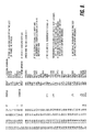
- Figure 8 shows a listing of a software program for a Motorola MC68HC05 processor corresponding to the flowchart in Figure 7.
- Control signals VR0 and VR1 may be generated at the outputs of a 2-bit counter. For example, incrementing the counter could produce a new value for signals VR0 and VR1 that would select a higher value for slicing reference level VS. Decrementing the counter would then select a lower slicing level.
- Figures 11 and 12 show an alternative embodiment for the apparatus in Figure 2.
- the arrangement in Figure 11 differs from that in Figure 2 in that low-pass filter 1160 and spike filter 1170 are included.
- Features 200 through 250 in Figure 11 correspond to features in Figure 2 that are numbered the same.
- Low-pass filter 1160 may be implemented using a single-pole RC-type low pass filter such as that shown in Figure 12A.
- the circuit shown in Figure 12A has a pole at 700KHz and reduces the amplitude of the 500KHz run-in clock sinewave by about 80 percent from the nominal 50 IRE value (see Figures 1 and 5) as can be seen in Figure 6.
- the reduction in the amplitude of the run-in clock relative to that of the data signal is advantageous because the range of RIC values is decreased correspondingly decreasing the adjustment range necessary for the slicing level.
- Spike filter 1170 is inserted into the signal path at the output of data slicer 230.
- Spike filter 1170 improves the accuracy with which the slicing level is set because, similarly to the action of the low-pass filter, the amplitude range of the RIC signal is decreased by eliminating the spike peaks on the RIC portion of the video waveform as shown in Figure 6.
- a digital embodiment of the spike filter is shown in Figure 12B.
- the circuit in Figure 12B eliminates from the data slicer output all pulses narrower than 280ns and passes all pulses wider than 420ns. As a result, with the slicer bias at a value near the positive or negative tips of the run-in clock in the video input, the resulting output pulses of the data slicer are eliminated by the spike filter if they are sufficiently narrow.
- the effect of the spike filter is demonstrated by the waveforms shown in Figure 6.
Landscapes
- Engineering & Computer Science (AREA)
- Multimedia (AREA)
- Signal Processing (AREA)
- Television Systems (AREA)
- Tone Control, Compression And Expansion, Limiting Amplitude (AREA)
- Testing, Inspecting, Measuring Of Stereoscopic Televisions And Televisions (AREA)
- Television Signal Processing For Recording (AREA)
- Control Of Amplification And Gain Control (AREA)
- Picture Signal Circuits (AREA)
Claims (13)
- Appareil pour le traitement d'un signal vidéo incluant une composante de signal de référence pendant des parties dudit signal vidéo, le dit appareil comprenant :des moyens (230) répondant audit signal vidéo (VIN) pour produire un signal de sortie ayant une première valeur quand ledit signal vidéo traverse un niveau de seuil (VS) dans un premier sens, et ayant une seconde valeur quand ledit signal vidéo traverse ledit niveau de seuil (VS) dans un autre sens.des moyens (220) pour modifier ledit niveau de seuil en réponse à un signal de commande (VR) .un compteur (250) répondant audit signal de sortie pour produire un premier comptage (RIC COUNT) représentatif du nombre de fois où ledit signal de sortie passe de ladite première valeur à ladite seconde valeur pendant chacune desdites parties dudit signal vidéo ;des moyens de commandes (200) pour déterminer après chacune desdites parties dudit signal vidéo si ledit compte est égal ou non à une valeur prédéterminée et pour générer ledit signal de commande (VR) afin de modifier ledit niveau de seuil (VS) lorsque ladite valeur de compte prédéterminée se produit moins fréquemment qu'une fréquence d'occurrence prédéterminée.
- Appareil selon la revendication 1 dans lequel :ledit signal de commande (VR) représente un second comptage ayant une valeur correspondante à une valeur dudit niveau de seuil ;lesdits moyens de commande (200) augmentent et diminuent ledit niveau de seuil en changeant ledit second comptage dans un seul sens.
- Appareil selon la revendication 1 dans lequelledit signal de commande (VR) comprend un signal numérique etledit niveau de seuil modifiant les moyens (220) comprenant un convertisseur numérique/analogique (360 ; R3, R4, R5, R6, R7) répondant audit signal numérique pour produire ledit niveau de seuil.
- Appareil selon la revendication 1 dans lequellesdits moyens de contrôle (200) produisent un second comptage ;ledit second comptage étant modifié dans un premier sens quand ledit premier comptage est égal à ladite valeur prédéterminée ;ledit second comptage étant modifié dans un second sens opposé au premier, quand ledit premier comptage n'est pas égal à ladite valeur prédéterminée ;et lesdits moyens de commande (200) génèrent ledit signal de commande (VR) pour modifier ledit niveau de seuil (VS), quand ledit second comptage est une valeur prédéterminée.
- Appareil de la revendication 4 dans lequelledit signal de commande (VR) représente un troisième comptage ayant une valeur correspondant à une valeur dudit niveau de seuil , etoù lesdits moyens de commande (200) augmentent et diminuent ledit niveau de seuil (VS) en modifiant ledit troisième comptage dans un seul sens.
- Appareil de la revendication 5 dans lequel ladite composante du signal de référence présente une variation d'amplitude périodique pendant lesdites parties dudit signal vidéo ; et ledit premier comptage représente un certain nombre de variation d'amplitude dans ledit signal de sortie correspondant à une desdites variations d'amplitude périodique dans ladite composante du signal de référence.
- Appareil selon la revendication 6 comprenant en outre des moyens de filtrage dans ledit cheminement du signal vidéo pour prévenir substantiellement des variations d'amplitude dans ledit signal vidéo autre que lesdites variations d'amplitude périodiques de ladite composante du signal de référence affectant ledit premier comptage.
- Appareil selon la revendication 7 dans lequel lesdits moyens de filtres comprennent un filtre passe-bas (1160) couplant ledit signal vidéo à une entrée dudit signal de sortie produisant des moyens, et un filtre de pointes de tension (1170) couplant ledit signal de sortie au compteur (250).
- Appareil selon la revendication 8 dans lequel ledit filtre de pointes d'impulsion (1170) est un filtre numérique.
- Appareil pour le traitement d'un signal vidéo (VIDEO) ayant une composante de signal de référence (horloge interne) incluse dans un intervalle de signal de différence pendant chaque occurrence d'une pluralité d'intervalles d'affichage horizontal (ligne 21) dudit signal vidéo (VIDEO) ledit appareil comprenant :des moyens (250) pour la détermination d'un nombre (RIC COUNT) de transitions de signal de ladite composante du signal de référence (horloge interne) qui croise un niveau de référence (VS) durant chacun desdits intervalles de signal de référence ; etdes moyens (200) pour modifier ledit niveau de référence (VS) après ladite pluralité d'intervalles d'affichage horizontal (ligne 21) en réponse audit nombre (RIC COUNT) étant inférieur à un nombre prédéterminé (3) pendant plus d'un desdits intervalles de signal de référence.
- Appareil pour le décodage d'informations auxiliaires incluses dans un signal vidéo (VIDEO) comprenant :un extracteur de données (230) pour fournir un signal de sortie (SLICED DATA) ayant des transitions de signal produites en réponse à des transitions de signal respectives dudit signal vidéo (VIDEO) qui croise un niveau de référence ( VS ; V1, V2, V3 ou V4) ;un compteur (250) répondant audit signal de sortie (données extraites) pour produire un premier comptage (RIC COUNT) représentant un certain nombre desdites transitions dudit signal de sortie (SLICED DATA) qui se produisent durant un intervalle ;des moyens (220 ; 360, R3-R9) répondant à la valeur d'un signal binaire (VR ; VR0, VR1) pour sélectionner ledit niveau de référence (VS ; V1, V2, V3 ou V4) ; etdes moyens de contrôle (200) pour générer ledit signal binaire (VR ; VR0, VR1) ayant un jeu de valeurs prédéterminées successives, et répondant audit premier comptage (RIC COUNT) pour modifier de façon sélective ledit signal binaire (VR ; VR0, VR1) pour assumer la valeur binaire successive afin de faire varier ledit niveau de référence (VS) lorsque le premier comptage (RIC COUNT) indique que le niveau de référence sélectionné (VS ; V1, V2, V3 ou, V4) est incorrect.
- Appareil de la revendication 11 dans lequel :ledit compteur (250) produit ledit premier comptage (RIC COUNT) pendant chaque intervalle inclus dans une pluralité d'intervalles ;ledit moyen de contrôle (200) comprend des moyens (µS) pour évaluer ledit premier comptage (RIC COUNT) après chaque intervalle inclus dans ladite pluralité d'intervalles et pour produire un second comptage (RICCNT3) représentant un certain nombre desdits intervalles durant lesquels ledit premier comptage (RIC COUNT) représente un nombre prédéterminé (3).
- Appareil selon la revendication 12 dans lequel lesdits moyens de contrôle (200) modifient ledit signal binaire (VR ; VR0, VR1) en réponse audit second comptage (RICCNT3) représentant un second nombre prédéterminé (0).
Applications Claiming Priority (3)
| Application Number | Priority Date | Filing Date | Title |
|---|---|---|---|
| GB9219505 | 1992-09-15 | ||
| GB929219505A GB9219505D0 (en) | 1992-09-15 | 1992-09-15 | Bias control apparatus for a data slicer in an auxiliary video information decoder |
| PCT/US1993/007163 WO1994007334A1 (fr) | 1992-09-15 | 1993-07-29 | Dispositif de commande de polarisation pour un extracteur de donnees dans un decodeur auxiliaire d'informations video |
Publications (2)
| Publication Number | Publication Date |
|---|---|
| EP0660989A1 EP0660989A1 (fr) | 1995-07-05 |
| EP0660989B1 true EP0660989B1 (fr) | 1998-01-07 |
Family
ID=10721941
Family Applications (1)
| Application Number | Title | Priority Date | Filing Date |
|---|---|---|---|
| EP93918512A Expired - Lifetime EP0660989B1 (fr) | 1992-09-15 | 1993-07-29 | Dispositif de commande de polarisation pour un extracteur de donnees dans un decodeur auxiliaire d'informations video |
Country Status (12)
| Country | Link |
|---|---|
| EP (1) | EP0660989B1 (fr) |
| JP (1) | JP3289107B2 (fr) |
| KR (1) | KR100341997B1 (fr) |
| CN (1) | CN1041484C (fr) |
| CA (1) | CA2143199C (fr) |
| DE (1) | DE69316226T2 (fr) |
| ES (1) | ES2111171T3 (fr) |
| GB (1) | GB9219505D0 (fr) |
| MX (1) | MX9305651A (fr) |
| MY (1) | MY110360A (fr) |
| SG (1) | SG94679A1 (fr) |
| WO (1) | WO1994007334A1 (fr) |
Families Citing this family (9)
| Publication number | Priority date | Publication date | Assignee | Title |
|---|---|---|---|---|
| KR0164563B1 (ko) * | 1993-07-23 | 1999-03-20 | 김광호 | 데이타 분리 회로 |
| US5748263A (en) * | 1995-03-07 | 1998-05-05 | Ball; Bradley E. | System for automatically producing infrared control signals |
| US5900913A (en) * | 1995-09-26 | 1999-05-04 | Thomson Consumer Electronics, Inc. | System providing standby operation of an auxiliary data decoder in a television receiver |
| CA2188707C (fr) | 1995-11-13 | 2000-08-01 | Aaron Hal Dinwiddie | Systeme servant a figer les sous-titres |
| EP1309190B1 (fr) * | 1996-09-11 | 2004-11-24 | Matsushita Electric Industrial Co., Ltd. | Dispositif pour commander l'affichage de données |
| JPH11199864A (ja) | 1997-10-10 | 1999-07-27 | Koto Gijutsu Kenkyuin Kenkyu Kumiai | 電気発光素子の製造方法 |
| JP3788253B2 (ja) * | 2001-03-12 | 2006-06-21 | ソニー株式会社 | データスライス回路 |
| US7688356B2 (en) | 2004-05-07 | 2010-03-30 | Nikon Corporation | Clamp level adjusting apparatus, electronic camera, image processing apparatus, and image processing program |
| US9313515B2 (en) | 2007-05-16 | 2016-04-12 | Thomson Licensing | Methods and apparatus for the use of slice groups in encoding multi-view video coding (MVC) information |
Family Cites Families (4)
| Publication number | Priority date | Publication date | Assignee | Title |
|---|---|---|---|---|
| EP0144457B1 (fr) * | 1983-12-07 | 1987-11-11 | Deutsche ITT Industries GmbH | Circuit d'écrêtage de données pour séparer et régénérer des signaux numériques de télétexte |
| US4620227A (en) * | 1984-01-30 | 1986-10-28 | Cybernetic Data Products | Data decoder |
| JPS6143886A (ja) * | 1984-08-08 | 1986-03-03 | Hitachi Ltd | デ−タ識別回路 |
| FR2652697A1 (fr) * | 1989-10-03 | 1991-04-05 | Sgs Thomson Microelectronics | Extracteur de donnees numeriques dans un signal video. |
-
1992
- 1992-09-15 GB GB929219505A patent/GB9219505D0/en active Pending
-
1993
- 1993-07-29 SG SG9602266A patent/SG94679A1/en unknown
- 1993-07-29 WO PCT/US1993/007163 patent/WO1994007334A1/fr not_active Ceased
- 1993-07-29 DE DE69316226T patent/DE69316226T2/de not_active Expired - Lifetime
- 1993-07-29 EP EP93918512A patent/EP0660989B1/fr not_active Expired - Lifetime
- 1993-07-29 ES ES93918512T patent/ES2111171T3/es not_active Expired - Lifetime
- 1993-07-29 JP JP50807294A patent/JP3289107B2/ja not_active Expired - Fee Related
- 1993-07-29 KR KR1019950701007A patent/KR100341997B1/ko not_active Expired - Fee Related
- 1993-07-29 CA CA002143199A patent/CA2143199C/fr not_active Expired - Fee Related
- 1993-09-04 MY MYPI93001799A patent/MY110360A/en unknown
- 1993-09-14 MX MX9305651A patent/MX9305651A/es not_active IP Right Cessation
- 1993-09-14 CN CN93117702A patent/CN1041484C/zh not_active Expired - Fee Related
Also Published As
| Publication number | Publication date |
|---|---|
| EP0660989A1 (fr) | 1995-07-05 |
| CA2143199C (fr) | 1999-07-06 |
| KR100341997B1 (ko) | 2003-02-17 |
| DE69316226D1 (de) | 1998-02-12 |
| MY110360A (en) | 1998-04-30 |
| CN1041484C (zh) | 1998-12-30 |
| SG94679A1 (en) | 2003-03-18 |
| DE69316226T2 (de) | 1998-04-16 |
| WO1994007334A1 (fr) | 1994-03-31 |
| CN1086067A (zh) | 1994-04-27 |
| JP3289107B2 (ja) | 2002-06-04 |
| ES2111171T3 (es) | 1998-03-01 |
| MX9305651A (es) | 1994-06-30 |
| JPH08501423A (ja) | 1996-02-13 |
| CA2143199A1 (fr) | 1994-03-31 |
| GB9219505D0 (en) | 1992-10-28 |
| KR950703836A (ko) | 1995-09-20 |
Similar Documents
| Publication | Publication Date | Title |
|---|---|---|
| US5666167A (en) | Bias control apparatus for a data slicer in an auxiliary video information decoder | |
| EP0572740B1 (fr) | Séparateur de données vidéo auxiliaires | |
| US5402488A (en) | Method and apparatus for modifying a video signal | |
| US5517249A (en) | Auxiliary video data slicer with adaptive slicing level capability | |
| US5463423A (en) | Auxiliary video data detector and data slicer | |
| CA2143199C (fr) | Commande de polarisation pour decoupeur de donnees incorpore a un decodeur de signaux video auxiliaires | |
| CA1287682C (fr) | Circuit de calage pour signaux video | |
| US4215371A (en) | Front porch clamping circuit | |
| US5619275A (en) | TV line and field detection apparatus with good noise immunity | |
| US4491870A (en) | Digital sync separator | |
| US4682087A (en) | Apparatus for controlling amplitude of vertical deflection signal | |
| US5784121A (en) | Vertical synchronisation signal detector | |
| JPS61172494A (ja) | バ−ストゲ−ト・パルス発生器 | |
| US5754251A (en) | Digital video vertical synchronization pulse detector | |
| CA2142697C (fr) | Detecteur de lignes et de trames de signal de television offrant une plus grande immunite au bruit | |
| EP0580287B1 (fr) | Méthode et dispositif pour détecter un signal de synchronisation d'image | |
| JP3232594B2 (ja) | 同期回路 | |
| CA2013532C (fr) | Circuit de separation de signaux de synchronisation | |
| JPS63116573A (ja) | 直流分再生回路 | |
| US5995158A (en) | Blanking signal generating control circuit of a video apparatus | |
| GB2238443A (en) | Video synchronising signal detection | |
| JPS6392170A (ja) | 垂直同期回路 |
Legal Events
| Date | Code | Title | Description |
|---|---|---|---|
| PUAI | Public reference made under article 153(3) epc to a published international application that has entered the european phase |
Free format text: ORIGINAL CODE: 0009012 |
|
| 17P | Request for examination filed |
Effective date: 19950301 |
|
| AK | Designated contracting states |
Kind code of ref document: A1 Designated state(s): DE ES FR GB IT |
|
| GRAG | Despatch of communication of intention to grant |
Free format text: ORIGINAL CODE: EPIDOS AGRA |
|
| 17Q | First examination report despatched |
Effective date: 19960711 |
|
| GRAG | Despatch of communication of intention to grant |
Free format text: ORIGINAL CODE: EPIDOS AGRA |
|
| GRAH | Despatch of communication of intention to grant a patent |
Free format text: ORIGINAL CODE: EPIDOS IGRA |
|
| GRAH | Despatch of communication of intention to grant a patent |
Free format text: ORIGINAL CODE: EPIDOS IGRA |
|
| GRAA | (expected) grant |
Free format text: ORIGINAL CODE: 0009210 |
|
| AK | Designated contracting states |
Kind code of ref document: B1 Designated state(s): DE ES FR GB IT |
|
| REF | Corresponds to: |
Ref document number: 69316226 Country of ref document: DE Date of ref document: 19980212 |
|
| REG | Reference to a national code |
Ref country code: ES Ref legal event code: FG2A Ref document number: 2111171 Country of ref document: ES Kind code of ref document: T3 |
|
| ITF | It: translation for a ep patent filed | ||
| ET | Fr: translation filed | ||
| PLBE | No opposition filed within time limit |
Free format text: ORIGINAL CODE: 0009261 |
|
| 26N | No opposition filed | ||
| REG | Reference to a national code |
Ref country code: GB Ref legal event code: IF02 |
|
| REG | Reference to a national code |
Ref country code: FR Ref legal event code: D6 |
|
| REG | Reference to a national code |
Ref country code: GB Ref legal event code: 746 Effective date: 20030103 |
|
| PGFP | Annual fee paid to national office [announced via postgrant information from national office to epo] |
Ref country code: ES Payment date: 20070801 Year of fee payment: 15 |
|
| PGFP | Annual fee paid to national office [announced via postgrant information from national office to epo] |
Ref country code: IT Payment date: 20070730 Year of fee payment: 15 |
|
| PG25 | Lapsed in a contracting state [announced via postgrant information from national office to epo] |
Ref country code: IT Free format text: LAPSE BECAUSE OF NON-PAYMENT OF DUE FEES Effective date: 20080729 |
|
| REG | Reference to a national code |
Ref country code: ES Ref legal event code: FD2A Effective date: 20080730 |
|
| PG25 | Lapsed in a contracting state [announced via postgrant information from national office to epo] |
Ref country code: ES Free format text: LAPSE BECAUSE OF NON-PAYMENT OF DUE FEES Effective date: 20080730 |
|
| PGFP | Annual fee paid to national office [announced via postgrant information from national office to epo] |
Ref country code: GB Payment date: 20100628 Year of fee payment: 18 Ref country code: FR Payment date: 20100802 Year of fee payment: 18 Ref country code: DE Payment date: 20100719 Year of fee payment: 18 |
|
| GBPC | Gb: european patent ceased through non-payment of renewal fee |
Effective date: 20110729 |
|
| REG | Reference to a national code |
Ref country code: FR Ref legal event code: ST Effective date: 20120330 |
|
| PG25 | Lapsed in a contracting state [announced via postgrant information from national office to epo] |
Ref country code: FR Free format text: LAPSE BECAUSE OF NON-PAYMENT OF DUE FEES Effective date: 20110801 Ref country code: DE Free format text: LAPSE BECAUSE OF NON-PAYMENT OF DUE FEES Effective date: 20120201 |
|
| REG | Reference to a national code |
Ref country code: DE Ref legal event code: R119 Ref document number: 69316226 Country of ref document: DE Effective date: 20120201 |
|
| PG25 | Lapsed in a contracting state [announced via postgrant information from national office to epo] |
Ref country code: GB Free format text: LAPSE BECAUSE OF NON-PAYMENT OF DUE FEES Effective date: 20110729 |