EP0661244A2 - Herstellung von Dünnschichtmaterialien - Google Patents
Herstellung von Dünnschichtmaterialien Download PDFInfo
- Publication number
- EP0661244A2 EP0661244A2 EP94114943A EP94114943A EP0661244A2 EP 0661244 A2 EP0661244 A2 EP 0661244A2 EP 94114943 A EP94114943 A EP 94114943A EP 94114943 A EP94114943 A EP 94114943A EP 0661244 A2 EP0661244 A2 EP 0661244A2
- Authority
- EP
- European Patent Office
- Prior art keywords
- layer
- grain size
- pyroelectric
- perovskite
- ferroelectric
- Prior art date
- Legal status (The legal status is an assumption and is not a legal conclusion. Google has not performed a legal analysis and makes no representation as to the accuracy of the status listed.)
- Withdrawn
Links
Images

Classifications
-
- C—CHEMISTRY; METALLURGY
- C04—CEMENTS; CONCRETE; ARTIFICIAL STONE; CERAMICS; REFRACTORIES
- C04B—LIME, MAGNESIA; SLAG; CEMENTS; COMPOSITIONS THEREOF, e.g. MORTARS, CONCRETE OR LIKE BUILDING MATERIALS; ARTIFICIAL STONE; CERAMICS; REFRACTORIES; TREATMENT OF NATURAL STONE
- C04B35/00—Shaped ceramic products characterised by their composition; Ceramics compositions; Processing powders of inorganic compounds preparatory to the manufacturing of ceramic products
- C04B35/01—Shaped ceramic products characterised by their composition; Ceramics compositions; Processing powders of inorganic compounds preparatory to the manufacturing of ceramic products based on oxide ceramics
- C04B35/46—Shaped ceramic products characterised by their composition; Ceramics compositions; Processing powders of inorganic compounds preparatory to the manufacturing of ceramic products based on oxide ceramics based on titanium oxides or titanates
- C04B35/462—Shaped ceramic products characterised by their composition; Ceramics compositions; Processing powders of inorganic compounds preparatory to the manufacturing of ceramic products based on oxide ceramics based on titanium oxides or titanates based on titanates
- C04B35/465—Shaped ceramic products characterised by their composition; Ceramics compositions; Processing powders of inorganic compounds preparatory to the manufacturing of ceramic products based on oxide ceramics based on titanium oxides or titanates based on titanates based on alkaline earth metal titanates
-
- C—CHEMISTRY; METALLURGY
- C04—CEMENTS; CONCRETE; ARTIFICIAL STONE; CERAMICS; REFRACTORIES
- C04B—LIME, MAGNESIA; SLAG; CEMENTS; COMPOSITIONS THEREOF, e.g. MORTARS, CONCRETE OR LIKE BUILDING MATERIALS; ARTIFICIAL STONE; CERAMICS; REFRACTORIES; TREATMENT OF NATURAL STONE
- C04B35/00—Shaped ceramic products characterised by their composition; Ceramics compositions; Processing powders of inorganic compounds preparatory to the manufacturing of ceramic products
- C04B35/622—Forming processes; Processing powders of inorganic compounds preparatory to the manufacturing of ceramic products
- C04B35/62218—Forming processes; Processing powders of inorganic compounds preparatory to the manufacturing of ceramic products obtaining ceramic films, e.g. by using temporary supports
Definitions
- This invention generally relates to the fabrication of thin film ferroelectric materials such as those used in non-volatile memory devices.
- the class of materials known as the perovskites exhibit several properties which make them useful in the microelectronics industry. Among these properties is a dielectric constant which can be several orders of magnitude greater than that of conventional insulators used in integrated circuits (e.g. SiO2 and Si3N4). This high dielectric constant can allow fabrication of very small capacitors which store charge in conventional DRAMs (dynamic random access memories), thereby increasing the density of memory cells.
- a dielectric constant which can be several orders of magnitude greater than that of conventional insulators used in integrated circuits (e.g. SiO2 and Si3N4). This high dielectric constant can allow fabrication of very small capacitors which store charge in conventional DRAMs (dynamic random access memories), thereby increasing the density of memory cells.
- the pyroelectric FOM is proportional to the ratio between the pyroelectric coefficient and dielectric constant.
- the pyroelectric coefficient is a function of the dielectric constant and the spontaneous polarization.
- Many perovskites exhibit a very large pyroelectric FOM, and if sufficiently large this pyroelectric property makes possible devices which are very sensitive to changes in temperature, including temperature changes caused by impinging electromagnetic radiation.
- Arrays of such pyroelectric detectors are now being fabricated which can image an infrared scene. These detectors do not require cryogenic cooling and are therefore economically feasible for consumer applications.
- the ferroelectric properties of perovskite materials are also useful in the microelectronics industry. Among those properties is the remanent polarization. The direction of this polarization may be switched by the application of an electric field to the material. The direction of this polarization may then be sensed electronically. The remanent polarization of these materials suggests that FRAMs (ferroelectric random access memories) could be constructed which would be non-volatile, i.e. the state (logic one or zero) of each memory element would be retained even if power is removed. Such devices, depending on the configuration, could in addition exhibit faster read/write cycles than conventional DRAMs.
- FRAMs ferrroelectric random access memories
- This invention is a method of forming thin-film perovskite structures which exhibit useful ferroelectric and pyroelectric properties.
- the perovskite materials are (1) any material exhibiting the well known perovskite crystal structure, typified by CaTiO3; and (2) compounds with structures which can be derived from the ideal cubic perovskite structure by way of small lattice distortions or omission of some atoms.
- Many perovskites have the chemical formula ABO3, where A is one or more monovalent, divalent or trivalent elements and B is one or more pentavalent, tetravalent, trivalent or divalent elements.
- perovskite materials To be useful in the fabrication of integrated circuit FRAMs, perovskite materials must exhibit large remanent polarization and small coercive voltage. To be useful in the fabrication of thin-film pyroelectric devices, perovskite materials must exhibit a large pyroelectric FOM. These properties should be present in thin-films of these materials.
- perovskite materials generally decrease as the grain size of the material is decreased.
- Bulk ceramic forms of perovskites generally have grain sizes on the order of 0.5 - 100 micrometers (mm), whereas typical thin-films have grain sizes of 0.02 - 0.5 mm.
- the useful properties are essentially absent for grain sizes below a critical grain size which is unique for each material and property.
- this invention overcomes the tradeoffs inherent in prior art techniques by changing the composition of the material in a way that decreases the grain size at which ferroelectric and/or pyroelectric properties abate.
- An improved ferroelectric material can be formed by adding lead to an original perovskite material having an original ferroelectric critical grain size, then forming a layer of the lead enhanced perovskite material having an average grain size less than the original ferroelectric critical grain size whereby the remanent polarization of the layer is substantially greater than the remanent polarization of the original perovskite material with an average grain size similar to the average grain size of the layer.
- the ferroelectric critical grain size means the largest grain size such that the remanent polarization starts to rapidly decrease with decreasing grain sizes (e.g. to a value of 1/2 the peak).
- an n-type lead enhanced perovskite material is doped with one or more acceptor dopants whereby the resistivity is substantially increased.
- a p-type lead enhanced perovskite material is doped with one or more donor dopants whereby the resistivity is substantially increased.
- the original perovskite material has a chemical composition ABO3, where A is one or more monovalent, divalent or trivalent elements (but, of course contains no lead), and B is one or more pentavalent, tetravalent, trivalent or divalent elements (but, again of course contains no lead).
- the pyroelectric properties (i.e. pyroelectric FOM) of thin film perovskite materials can be enhanced by adding lead.
- a layer of an improved pyroelectric material can be made by adding lead to an "original" perovskite material (which would have had a certain original pyroelectric critical grain size), and the layer of the lead enhanced perovskite material can have an average grain size less than the "original" pyroelectric critical grain size whereby the pyroelectric FOM of the layer is substantially greater than the pyroelectric FOM of the "original" perovskite material would have at that same grain size.
- the pyroelectric critical grain size as used herein, means the largest grain size such that the pyroelectric FOM starts to rapidly decrease with decreasing grain sizes.
- the layer of perovskite is interposed between a first conductive layer and a second conductive layer.
- the grain size less than 0.5 micron and the layer is formed at a temperature of less than 600 degrees C.
- compositions and values for "x" include: where A principally comprises strontium, B principally comprises titanium, and x is approximately 0.35; where A principally comprises strontium, B principally comprises titanium, and x is approximately 0.1-0.4; where A principally comprises strontium, B principally comprises titanium, and x is approximately 0.3-0.4; where A principally comprises strontium, B principally comprises titanium, and x is approximately 0.3; where A principally comprises strontium, B principally comprises titanium, and x is approximately 0.2; and where A principally comprises barium and strontium, B principally comprises titanium, and x is approximately 0.1 - 0.4.
- Materials and uses include: where the perovskite layer is doped or undoped barium lead titinate and the layer is utilized as a ferroelectric; where the perovskite layer is strontium lead titanate and the layer is utilized as a pyroelectric; where the perovskite layer is doped or undoped strontium lead titinate and the layer is utilized as a pyroelectric as layer for a high dielectric capacitor; and where the perovskite layer is barium lead titinate with limited amounts of strontium titanate and barium zirconate and the layer is utilized as a pyroelectric using the lower ferroelectric-ferroelectric phase transition of the layer and x is approximately 0.1-0.4.
- an n-type lead enhanced perovskite material is doped with one or more acceptor dopants whereby the resistivity is substantially increased.
- a p-type lead enhanced perovskite material is doped with one or more donor dopants whereby the resistivity is substantially increased.
- the original perovskite material has a chemical composition ABO3, where A is one or more monovalent, divalent or trivalent elements, and B is one or more pentavalent, tetravalent, trivalent or divalent elements.
- Structures containing these improved ferroelectric and pyroelectric materials can include a layer of lead enhanced perovskite material with average grain size less than the original ferroelectric or pyroelectric critical grain size formed on the surface of a substrate.
- Other structures include such a layer of lead enhanced material interposed between two electrically conducting layers.
- the materials presented may find use in many structures used in semiconductor circuitry, such as capacitors, transistors, non-volatile memory cells, pixels for electro-magnetic radiation detecting arrays, and other electrooptic applications. Devices which exploit the piezoelectric properties of many of these materials will benefit from this invention.
- the advantages of this invention include substantially increased remanent polarization for perovskite materials formed with grain sizes typically found in thin films. This invention also serves to preserve the pyroelectric FOM in thin films of perovskite materials. In addition, the resistivity is generally increased by the methods presented.
- the useful ferroelectric and pyroelectric properties of a perovskite material generally decrease as the grain size of the material is decreased.
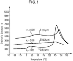
- the dielectric constant of undoped barium titanate (BT) varies with temperature and grain size.
- the dielectric constant varies rapidly near the Curie temperature (approximately 130 °C), but is less variable at other temperatures.
- the peak becomes less pronounced, the dielectric constant below the Curie temperature increases and varies less with temperature.
- the dielectric constant decreases for all temperatures and is essentially constant with respect to temperature.
- the dielectric constant has a pronounced peak at the Curie temperature. As the grain size decreases, the dielectric constant below the Curie temperature increases and the peak is less pronounced.
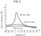
- BST barium strontium titanate
- the rate of change of the dielectric constant with temperature is large, the pyroelectric FOM is also large.
- the rate of change of the dielectric constant decreases below some grain size, i.e. the slope of the curve becomes smaller as the grain size is decreased below some value.
- That value for barium titanate is approximately 6.8 mm according to the data represented by Figure 1.
- Figure 3 illustrates, that value for barium strontium titanate is approximately 10 mm.
- the pyroelectric FOM of pyroelectric perovskite materials decreases rapidly below some grain size.
- the pyroelectric critical grain size means the largest grain size such that the pyroelectric FOM starts to rapidly decrease with decreasing grain sizes (e.g. to a value of 1/2 the peak).
- the typical grain size present in most thin-film perovskites is generally much smaller than the PCGS, causing the pyroelectric properties of thin films to be small or nonexistent.
- the grain size of a thin film perovskite must be larger than the PCGS in order for the film to possess useful pyroelectric properties. A method to decrease the PCGS below typical thin film grain sizes is desirable.
- the useful ferroelectric properties of perovskites also decrease for decreasing grain sizes.
- the remanent polarization exhibited by barium zirconate titanate is 18 mC/cm2 for grain sizes larger than 100 mm.
- the remanent polarization has been measured at 6 mC/cm2.
- the remanent polarization rapidly decreases until it is essentially gone.
- the remanent polarization of ferroelectric perovskite materials decreases rapidly below some grain size.
- the typical grain size present in most thin-films is generally much smaller than the FCGS, thus the ferroelectric properties of such perovskites thin films would be small or nonexistent, and as such perovskites have not been used in thin films.
- the grain size of a thin film perovskite must be larger than the FCGS in order for the film to possess useful ferroelectric properties. Thus a method to decrease the FCGS below typical thin film grain sizes is desirable.
- Lead generally decreases the pyroelectric critical grain size and the ferroelectric critical grain size of perovskite materials. This effect is not taught by the prior art and its mechanism and explanation are uncertain. Lead may be added to a perovskite material which, as normally previously used, contained essentially no lead. Alternately, lead may be added to a perovskite material which initially contains some lead. In either case, the critical grains sizes (FCGS and PCGS) of the lead enhanced materials are less than the critical grain sizes of the original material.
- acceptor dopants increase the resistivity of n-type lead enhanced perovskite materials. Therefore, another aspect of this invention is acceptor doping of n-type lead enhanced ferroelectric and pyroelectric perovskite materials.
- an element or ion is an acceptor dopant if (1) it replaces an atom in the crystal lattice and has a lesser number of valence electrons than the atom it replaces or (2) it exists interstitially and its outer electron shell is more than half full. Intermediate cases are uncertain and may be determined empirically. For example, some elements behave as acceptor dopants in (1) when their valence is the same as the atom replaced. Likewise, in (2) some elements behave as acceptor dopants when their valence shell is exactly half full.
- donor dopants increase the resistivity of p-type lead enhanced perovskite materials. Therefore, another aspect of this invention is donor doping of p-type lead enhanced ferroelectric and pyroelectric perovskite materials.
- an element or ion is a donor dopant if (1) it replaces an atom in the crystal lattice and has a greater number of valence electrons than the atom it replaces or (2) it exists interstitially and its outer electron shell is less than half full. Intermediate cases are uncertain and may be determined empirically. For example, some elements behave as donor dopants in (1) when their valence is the same as the atom replaced. Likewise, in (2) some elements behave as donor dopants when their valence shell is exactly half full.
- a dopant is a species which is intentionally introduced into an intrinsic material in order to produce some effect. Unintentional impurities which exist in concentrations below approximately 0.1 mole percent are not generally considered dopants. Accordingly, in the context of this invention, an intrinsic perovskite material is a perovskite material in which impurities which behave as acceptor dopants, if present, exist at concentrations below approximately 0.1 mole percent.
- material with the nominal composition (Sr 0.65 ,Pb 0.35 )TiO3 is prepared by combining constituents in a solution, then calcining the solution in bulk. The bulk ceramic is then ground, pressed, and sintered to produce a ceramic with density at least 95% of theoretical density.
- the ceramic is mechanically polished and thinned to 250 mm thickness.
- Metallization is applied to form test capacitors.
- the average grain size of the material produced was 0.8 mm as measured by the line intercept method.
- the peak dielectric constant (the dielectric constant at the Curie temperature) was greater than 10,000, and varied rapidly with respect to temperature. This behavior indicates that the pyroelectric critical grain size of this material is less than 0.8 mm.
- the Curie temperature of (Sr 0.65 ,Pb 0.35 )TiO3 is ⁇ 300 K while the curie temperature of pure SrTiO3 is ⁇ 7 K below which the SrTiO3 becomes antiferroelectric and not ferroelectric.
- the ferroelectric critical grain size of SrTiO3 is therefore dependent on the measurement temperature and does not exist at room temperature since the SrTiO3 is never ferroelectric. It is therefore very difficult to compare the FCGS of (Sr 0.65 ,Pb 0.35 )TiO3 with SrTiO3.
- BST and the SPT are just a subset of the compounds (Sr 1-x-y ,Ba x ,Pb y )TiO3 (SBPT). Since (Sr 0.65 ,Pb 0.35 )TiO3 and (Ba 0.70 ,Sr 0.30 )TiO3 have the same curie temperature the improvement in the CGS of SPT compared to BST must be due to the substitution of the Pb for Ba and Sr. As mentioned previously, the explanation for why the substitution of Pb on the A site improve the ferroelectric and pyroelectric properties at small grain sizes is unclear.
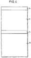
- FIG. 4 A structure using such a perovskite is shown in Figure 4.
- the layer of perovskite 12 is interposed between a first conductive layer 14 and a second conductive layer 16. Perovskite 12 is shown on the first conductive layer 14 which is in turn on a substrate 18.
- Internal and external connections can be ohmic, capacitive, direct or indirect, via intervening circuits or otherwise. Implementation is contemplated in discrete components or fully integrated circuits in silicon, gallium arsenide, or other electronic materials families, as well as in optical-based or other technology-based forms and embodiments.
Landscapes
- Engineering & Computer Science (AREA)
- Chemical & Material Sciences (AREA)
- Ceramic Engineering (AREA)
- Manufacturing & Machinery (AREA)
- Organic Chemistry (AREA)
- Structural Engineering (AREA)
- Materials Engineering (AREA)
- Inorganic Chemistry (AREA)
- Inorganic Insulating Materials (AREA)
- Compositions Of Oxide Ceramics (AREA)
- Inorganic Compounds Of Heavy Metals (AREA)
- Semiconductor Memories (AREA)
- Non-Volatile Memory (AREA)
Applications Claiming Priority (2)
| Application Number | Priority Date | Filing Date | Title |
|---|---|---|---|
| US12784893A | 1993-09-28 | 1993-09-28 | |
| US127848 | 1993-09-28 |
Publications (2)
| Publication Number | Publication Date |
|---|---|
| EP0661244A2 true EP0661244A2 (de) | 1995-07-05 |
| EP0661244A3 EP0661244A3 (de) | 1996-09-11 |
Family
ID=22432277
Family Applications (1)
| Application Number | Title | Priority Date | Filing Date |
|---|---|---|---|
| EP94114943A Withdrawn EP0661244A3 (de) | 1993-09-28 | 1994-09-22 | Herstellung von Dünnschichtmaterialien. |
Country Status (2)
| Country | Link |
|---|---|
| EP (1) | EP0661244A3 (de) |
| JP (1) | JPH07215762A (de) |
Cited By (1)
| Publication number | Priority date | Publication date | Assignee | Title |
|---|---|---|---|---|
| US7365327B2 (en) | 2003-03-07 | 2008-04-29 | Fujitsu Limited | Electromagnetic radiation sensor and method for fabricating the same |
Family Cites Families (5)
| Publication number | Priority date | Publication date | Assignee | Title |
|---|---|---|---|---|
| GB2193713B (en) * | 1986-07-14 | 1990-12-05 | Cabot Corp | Method of producing perovskite-type compounds. |
| JPS63319214A (ja) * | 1987-06-23 | 1988-12-27 | Ube Ind Ltd | コンデンサ−材料用粉末 |
| US5079200A (en) * | 1990-08-23 | 1992-01-07 | The United States Of America As Represented By The Secretary Of The Army | Detector material for uncooled thermal imaging devices |
| US5164882A (en) * | 1990-12-17 | 1992-11-17 | Kabushiki Kaisha Toshiba | Ceramic capacitor |
| EP0571949A1 (de) * | 1992-05-29 | 1993-12-01 | Texas Instruments Incorporated | Perovskite reich an Blei für Dünnfilm-Dielektrika |
-
1994
- 1994-09-22 EP EP94114943A patent/EP0661244A3/de not_active Withdrawn
- 1994-09-27 JP JP23160594A patent/JPH07215762A/ja active Pending
Cited By (1)
| Publication number | Priority date | Publication date | Assignee | Title |
|---|---|---|---|---|
| US7365327B2 (en) | 2003-03-07 | 2008-04-29 | Fujitsu Limited | Electromagnetic radiation sensor and method for fabricating the same |
Also Published As
| Publication number | Publication date |
|---|---|
| JPH07215762A (ja) | 1995-08-15 |
| EP0661244A3 (de) | 1996-09-11 |
Similar Documents
| Publication | Publication Date | Title |
|---|---|---|
| US5760432A (en) | Thin film strained layer ferroelectric capacitors | |
| US11121139B2 (en) | Hafnium oxide and zirconium oxide based ferroelectric devices with textured iridium bottom electrodes | |
| US6642539B2 (en) | Epitaxial template and barrier for the integration of functional thin film metal oxide heterostructures on silicon | |
| Naoko Yanase et al. | Thickness dependence of ferroelectricity in heteroepitaxial BaTiO3 thin film capacitors | |
| US5418389A (en) | Field-effect transistor with perovskite oxide channel | |
| KR100707201B1 (ko) | 강유전체 캐패시터, 그 제조 방법 및 강유전체 메모리 소자 | |
| JPH09186300A (ja) | 半導体メモリセルのキャパシタ構造およびその形成方法 | |
| JPH10270654A (ja) | 半導体記憶装置 | |
| EP0571948A1 (de) | Donatoren-dotierte Perovskite für Dünnfilm-Dielektrika | |
| US5168420A (en) | Ferroelectrics epitaxially grown on superconducting substrates | |
| Udayakumar et al. | Polarization reversal and high dielectric permittivity in lead magnesium niobate titanate thin films | |
| Guerrero et al. | Growth and characterization of epitaxial ferroelectric PbZrxTi1− xO3 thin film capacitors with SrRuO3 electrodes for non-volatile memory applications | |
| EP2076910A2 (de) | Ferroelektrischer varaktor mit verbessertem abstimmbereich | |
| US5504330A (en) | Lead substitured perovskites for thin-film pyroelectric devices | |
| Abe et al. | Modification of ferroelectricity in heteroepitaxial (Ba, Sr) TiO3 films for non-volatile memory applications | |
| US5721043A (en) | Method of forming improved thin film dielectrics by Pb doping | |
| KR100807518B1 (ko) | 온도 보상형 강유전성 커패시터 장치 및 그 제조 | |
| US6432473B1 (en) | PB substituted perovskites for thin films dielectrics | |
| US5888659A (en) | Donor doped perovskites for thin-film ferroelectric and pyroelectric devices | |
| JPH08335672A (ja) | 強誘電体不揮発性メモリ | |
| EP0607501A2 (de) | Verbesserungen von, oder in Zusammenhang mit, Dünnschichten aus ferroelektrischen Materialien | |
| EP0661244A2 (de) | Herstellung von Dünnschichtmaterialien | |
| JP3138128B2 (ja) | 誘電体薄膜構造物 | |
| JPH1187634A (ja) | 薄膜キャパシタ | |
| Li et al. | The effect of bottom electrode on structure and electrical properties of BaZr0. 15Ti0. 85O3 films on SrTiO3 substrates |
Legal Events
| Date | Code | Title | Description |
|---|---|---|---|
| PUAI | Public reference made under article 153(3) epc to a published international application that has entered the european phase |
Free format text: ORIGINAL CODE: 0009012 |
|
| AK | Designated contracting states |
Kind code of ref document: A2 Designated state(s): DE FR GB IT NL |
|
| PUAL | Search report despatched |
Free format text: ORIGINAL CODE: 0009013 |
|
| AK | Designated contracting states |
Kind code of ref document: A3 Designated state(s): DE FR GB IT NL |
|
| 17P | Request for examination filed |
Effective date: 19970424 |
|
| 17Q | First examination report despatched |
Effective date: 19971208 |
|
| STAA | Information on the status of an ep patent application or granted ep patent |
Free format text: STATUS: THE APPLICATION HAS BEEN WITHDRAWN |
|
| 18W | Application withdrawn |
Withdrawal date: 19980629 |