EP0663693A1 - Integrierte Schaltung mit niedrigem Wärmewiderstand - Google Patents
Integrierte Schaltung mit niedrigem Wärmewiderstand Download PDFInfo
- Publication number
- EP0663693A1 EP0663693A1 EP19940118870 EP94118870A EP0663693A1 EP 0663693 A1 EP0663693 A1 EP 0663693A1 EP 19940118870 EP19940118870 EP 19940118870 EP 94118870 A EP94118870 A EP 94118870A EP 0663693 A1 EP0663693 A1 EP 0663693A1
- Authority
- EP
- European Patent Office
- Prior art keywords
- transistor
- integrated circuit
- ground plane
- substrate
- forming
- Prior art date
- Legal status (The legal status is an assumption and is not a legal conclusion. Google has not performed a legal analysis and makes no representation as to the accuracy of the status listed.)
- Withdrawn
Links
Images






Classifications
-
- H—ELECTRICITY
- H10—SEMICONDUCTOR DEVICES; ELECTRIC SOLID-STATE DEVICES NOT OTHERWISE PROVIDED FOR
- H10D—INORGANIC ELECTRIC SEMICONDUCTOR DEVICES
- H10D64/00—Electrodes of devices having potential barriers
- H10D64/20—Electrodes characterised by their shapes, relative sizes or dispositions
- H10D64/23—Electrodes carrying the current to be rectified, amplified, oscillated or switched, e.g. sources, drains, anodes or cathodes
- H10D64/251—Source or drain electrodes for field-effect devices
- H10D64/252—Source or drain electrodes for field-effect devices for vertical or pseudo-vertical devices
-
- H—ELECTRICITY
- H10—SEMICONDUCTOR DEVICES; ELECTRIC SOLID-STATE DEVICES NOT OTHERWISE PROVIDED FOR
- H10D—INORGANIC ELECTRIC SEMICONDUCTOR DEVICES
- H10D10/00—Bipolar junction transistors [BJT]
- H10D10/80—Heterojunction BJTs
- H10D10/821—Vertical heterojunction BJTs
-
- H—ELECTRICITY
- H10—SEMICONDUCTOR DEVICES; ELECTRIC SOLID-STATE DEVICES NOT OTHERWISE PROVIDED FOR
- H10W—GENERIC PACKAGES, INTERCONNECTIONS, CONNECTORS OR OTHER CONSTRUCTIONAL DETAILS OF DEVICES COVERED BY CLASS H10
- H10W20/00—Interconnections in chips, wafers or substrates
- H10W20/01—Manufacture or treatment
- H10W20/021—Manufacture or treatment of interconnections within wafers or substrates
- H10W20/023—Manufacture or treatment of interconnections within wafers or substrates the interconnections being through-semiconductor vias
- H10W20/0234—Manufacture or treatment of interconnections within wafers or substrates the interconnections being through-semiconductor vias comprising etching via holes that stop on pads or on electrodes
-
- H—ELECTRICITY
- H10—SEMICONDUCTOR DEVICES; ELECTRIC SOLID-STATE DEVICES NOT OTHERWISE PROVIDED FOR
- H10W—GENERIC PACKAGES, INTERCONNECTIONS, CONNECTORS OR OTHER CONSTRUCTIONAL DETAILS OF DEVICES COVERED BY CLASS H10
- H10W20/00—Interconnections in chips, wafers or substrates
- H10W20/01—Manufacture or treatment
- H10W20/021—Manufacture or treatment of interconnections within wafers or substrates
- H10W20/023—Manufacture or treatment of interconnections within wafers or substrates the interconnections being through-semiconductor vias
- H10W20/0242—Manufacture or treatment of interconnections within wafers or substrates the interconnections being through-semiconductor vias comprising etching via holes from the back sides of the chips, wafers or substrates
-
- H—ELECTRICITY
- H10—SEMICONDUCTOR DEVICES; ELECTRIC SOLID-STATE DEVICES NOT OTHERWISE PROVIDED FOR
- H10W—GENERIC PACKAGES, INTERCONNECTIONS, CONNECTORS OR OTHER CONSTRUCTIONAL DETAILS OF DEVICES COVERED BY CLASS H10
- H10W20/00—Interconnections in chips, wafers or substrates
- H10W20/20—Interconnections within wafers or substrates, e.g. through-silicon vias [TSV]
-
- H—ELECTRICITY
- H10—SEMICONDUCTOR DEVICES; ELECTRIC SOLID-STATE DEVICES NOT OTHERWISE PROVIDED FOR
- H10W—GENERIC PACKAGES, INTERCONNECTIONS, CONNECTORS OR OTHER CONSTRUCTIONAL DETAILS OF DEVICES COVERED BY CLASS H10
- H10W20/00—Interconnections in chips, wafers or substrates
- H10W20/40—Interconnections external to wafers or substrates, e.g. back-end-of-line [BEOL] metallisations or vias connecting to gate electrodes
- H10W20/482—Interconnections external to wafers or substrates, e.g. back-end-of-line [BEOL] metallisations or vias connecting to gate electrodes for individual devices provided for in groups H10D8/00 - H10D48/00, e.g. for power transistors
- H10W20/483—Interconnections over air gaps, e.g. air bridges
-
- H—ELECTRICITY
- H10—SEMICONDUCTOR DEVICES; ELECTRIC SOLID-STATE DEVICES NOT OTHERWISE PROVIDED FOR
- H10W—GENERIC PACKAGES, INTERCONNECTIONS, CONNECTORS OR OTHER CONSTRUCTIONAL DETAILS OF DEVICES COVERED BY CLASS H10
- H10W20/00—Interconnections in chips, wafers or substrates
- H10W20/40—Interconnections external to wafers or substrates, e.g. back-end-of-line [BEOL] metallisations or vias connecting to gate electrodes
- H10W20/482—Interconnections external to wafers or substrates, e.g. back-end-of-line [BEOL] metallisations or vias connecting to gate electrodes for individual devices provided for in groups H10D8/00 - H10D48/00, e.g. for power transistors
- H10W20/484—Interconnections having extended contours, e.g. pads having mesh shape or interconnections comprising connected parallel stripes
-
- H—ELECTRICITY
- H10—SEMICONDUCTOR DEVICES; ELECTRIC SOLID-STATE DEVICES NOT OTHERWISE PROVIDED FOR
- H10W—GENERIC PACKAGES, INTERCONNECTIONS, CONNECTORS OR OTHER CONSTRUCTIONAL DETAILS OF DEVICES COVERED BY CLASS H10
- H10W44/00—Electrical arrangements for controlling or matching impedance
- H10W44/20—Electrical arrangements for controlling or matching impedance at high-frequency [HF] or radio frequency [RF]
-
- H—ELECTRICITY
- H10—SEMICONDUCTOR DEVICES; ELECTRIC SOLID-STATE DEVICES NOT OTHERWISE PROVIDED FOR
- H10W—GENERIC PACKAGES, INTERCONNECTIONS, CONNECTORS OR OTHER CONSTRUCTIONAL DETAILS OF DEVICES COVERED BY CLASS H10
- H10W72/00—Interconnections or connectors in packages
- H10W72/50—Bond wires
-
- H—ELECTRICITY
- H10—SEMICONDUCTOR DEVICES; ELECTRIC SOLID-STATE DEVICES NOT OTHERWISE PROVIDED FOR
- H10W—GENERIC PACKAGES, INTERCONNECTIONS, CONNECTORS OR OTHER CONSTRUCTIONAL DETAILS OF DEVICES COVERED BY CLASS H10
- H10W72/00—Interconnections or connectors in packages
- H10W72/90—Bond pads, in general
-
- H—ELECTRICITY
- H10—SEMICONDUCTOR DEVICES; ELECTRIC SOLID-STATE DEVICES NOT OTHERWISE PROVIDED FOR
- H10W—GENERIC PACKAGES, INTERCONNECTIONS, CONNECTORS OR OTHER CONSTRUCTIONAL DETAILS OF DEVICES COVERED BY CLASS H10
- H10W70/00—Package substrates; Interposers; Redistribution layers [RDL]
- H10W70/60—Insulating or insulated package substrates; Interposers; Redistribution layers
- H10W70/67—Insulating or insulated package substrates; Interposers; Redistribution layers characterised by their insulating layers or insulating parts
- H10W70/68—Shapes or dispositions thereof
- H10W70/682—Shapes or dispositions thereof comprising holes having chips therein
-
- H—ELECTRICITY
- H10—SEMICONDUCTOR DEVICES; ELECTRIC SOLID-STATE DEVICES NOT OTHERWISE PROVIDED FOR
- H10W—GENERIC PACKAGES, INTERCONNECTIONS, CONNECTORS OR OTHER CONSTRUCTIONAL DETAILS OF DEVICES COVERED BY CLASS H10
- H10W70/00—Package substrates; Interposers; Redistribution layers [RDL]
- H10W70/60—Insulating or insulated package substrates; Interposers; Redistribution layers
- H10W70/67—Insulating or insulated package substrates; Interposers; Redistribution layers characterised by their insulating layers or insulating parts
- H10W70/68—Shapes or dispositions thereof
- H10W70/685—Shapes or dispositions thereof comprising multiple insulating layers
-
- H—ELECTRICITY
- H10—SEMICONDUCTOR DEVICES; ELECTRIC SOLID-STATE DEVICES NOT OTHERWISE PROVIDED FOR
- H10W—GENERIC PACKAGES, INTERCONNECTIONS, CONNECTORS OR OTHER CONSTRUCTIONAL DETAILS OF DEVICES COVERED BY CLASS H10
- H10W72/00—Interconnections or connectors in packages
- H10W72/20—Bump connectors, e.g. solder bumps or copper pillars; Dummy bumps; Thermal bumps
- H10W72/29—Bond pads specially adapted therefor
-
- H—ELECTRICITY
- H10—SEMICONDUCTOR DEVICES; ELECTRIC SOLID-STATE DEVICES NOT OTHERWISE PROVIDED FOR
- H10W—GENERIC PACKAGES, INTERCONNECTIONS, CONNECTORS OR OTHER CONSTRUCTIONAL DETAILS OF DEVICES COVERED BY CLASS H10
- H10W72/00—Interconnections or connectors in packages
- H10W72/50—Bond wires
- H10W72/531—Shapes of wire connectors
- H10W72/536—Shapes of wire connectors the connected ends being ball-shaped
-
- H—ELECTRICITY
- H10—SEMICONDUCTOR DEVICES; ELECTRIC SOLID-STATE DEVICES NOT OTHERWISE PROVIDED FOR
- H10W—GENERIC PACKAGES, INTERCONNECTIONS, CONNECTORS OR OTHER CONSTRUCTIONAL DETAILS OF DEVICES COVERED BY CLASS H10
- H10W72/00—Interconnections or connectors in packages
- H10W72/50—Bond wires
- H10W72/59—Bond pads specially adapted therefor
-
- H—ELECTRICITY
- H10—SEMICONDUCTOR DEVICES; ELECTRIC SOLID-STATE DEVICES NOT OTHERWISE PROVIDED FOR
- H10W—GENERIC PACKAGES, INTERCONNECTIONS, CONNECTORS OR OTHER CONSTRUCTIONAL DETAILS OF DEVICES COVERED BY CLASS H10
- H10W72/00—Interconnections or connectors in packages
- H10W72/851—Dispositions of multiple connectors or interconnections
- H10W72/874—On different surfaces
- H10W72/884—Die-attach connectors and bond wires
-
- H—ELECTRICITY
- H10—SEMICONDUCTOR DEVICES; ELECTRIC SOLID-STATE DEVICES NOT OTHERWISE PROVIDED FOR
- H10W—GENERIC PACKAGES, INTERCONNECTIONS, CONNECTORS OR OTHER CONSTRUCTIONAL DETAILS OF DEVICES COVERED BY CLASS H10
- H10W72/00—Interconnections or connectors in packages
- H10W72/90—Bond pads, in general
- H10W72/921—Structures or relative sizes of bond pads
- H10W72/923—Bond pads having multiple stacked layers
-
- H—ELECTRICITY
- H10—SEMICONDUCTOR DEVICES; ELECTRIC SOLID-STATE DEVICES NOT OTHERWISE PROVIDED FOR
- H10W—GENERIC PACKAGES, INTERCONNECTIONS, CONNECTORS OR OTHER CONSTRUCTIONAL DETAILS OF DEVICES COVERED BY CLASS H10
- H10W72/00—Interconnections or connectors in packages
- H10W72/90—Bond pads, in general
- H10W72/951—Materials of bond pads
-
- H—ELECTRICITY
- H10—SEMICONDUCTOR DEVICES; ELECTRIC SOLID-STATE DEVICES NOT OTHERWISE PROVIDED FOR
- H10W—GENERIC PACKAGES, INTERCONNECTIONS, CONNECTORS OR OTHER CONSTRUCTIONAL DETAILS OF DEVICES COVERED BY CLASS H10
- H10W72/00—Interconnections or connectors in packages
- H10W72/90—Bond pads, in general
- H10W72/951—Materials of bond pads
- H10W72/952—Materials of bond pads comprising metals or metalloids, e.g. PbSn, Ag or Cu
-
- H—ELECTRICITY
- H10—SEMICONDUCTOR DEVICES; ELECTRIC SOLID-STATE DEVICES NOT OTHERWISE PROVIDED FOR
- H10W—GENERIC PACKAGES, INTERCONNECTIONS, CONNECTORS OR OTHER CONSTRUCTIONAL DETAILS OF DEVICES COVERED BY CLASS H10
- H10W90/00—Package configurations
- H10W90/701—Package configurations characterised by the relative positions of pads or connectors relative to package parts
- H10W90/751—Package configurations characterised by the relative positions of pads or connectors relative to package parts of bond wires
- H10W90/754—Package configurations characterised by the relative positions of pads or connectors relative to package parts of bond wires between a chip and a stacked insulating package substrate, interposer or RDL
-
- Y—GENERAL TAGGING OF NEW TECHNOLOGICAL DEVELOPMENTS; GENERAL TAGGING OF CROSS-SECTIONAL TECHNOLOGIES SPANNING OVER SEVERAL SECTIONS OF THE IPC; TECHNICAL SUBJECTS COVERED BY FORMER USPC CROSS-REFERENCE ART COLLECTIONS [XRACs] AND DIGESTS
- Y10—TECHNICAL SUBJECTS COVERED BY FORMER USPC
- Y10S—TECHNICAL SUBJECTS COVERED BY FORMER USPC CROSS-REFERENCE ART COLLECTIONS [XRACs] AND DIGESTS
- Y10S438/00—Semiconductor device manufacturing: process
- Y10S438/928—Front and rear surface processing
Definitions
- the invention relates to electronic devices, and, more particularly, to integrated circuit thermal dissipation structures and methods of fabrication.
- the ratio of the rise in junction temperature to the wattage being dissipated is termed the thermal resistance (thermal impedance) and typical values are 20 °C/W for a silicon integrated circuit in a 140-pin plastic quad flatpack; 150 °C/W for a silicon integrated circuit in an 8-pin small outline plastic package; and 10 °C/W for a 10 W gallium arsenide (GaAs) heterojunction bipolar transistor (HBT) in a monolithic microwave integrated circuit (MMIC).
- the thermal resistance scales with the chip area, so accurate comparisons would require comparable size chips.
- Figure 1 illustrates in cross sectional elevation view a portion of MMIC 100 showing air bridge 102 connecting two source regions of MESFET 104 through a via to ground plane 106 plus microstrip transmission line 108 and wire bonding 110 to lead 122 on alumina substrate 120 which may connect to a coaxial cable.
- the ground plane typically abuts a heat sink, and that the GaAs die for MMIC 100 is about 100 mm thick.
- the high thermal resistance for GaAs-based HBTs and MESFETs in part reflects the fact that silicon has three times the thermal conductivity of GaAs.
- Heat dissipation limitations for GaAs-based HBTs remain a problem for MMICs and, in effect, require devices be spread out over a large area in order to lower the thermal resistance. This limits integration density.
- Flip-chip bonding for silicon integrated circuits allows for a higher density of interconnections than with traditional wire bonding and tape automated bonding (TAB).
- TAB tape automated bonding
- solder bumps on the bonding pads on the frontside of a die are aligned with solder-wettable metallization on the carrier substrate, and a solder reflow forms all of the solder bonds simultaneously.
- Pickering et al., 8 J.Vac.Sci.Tech.A 1503 (1990) discusses the reflow bonding process.
- the flip-chip bond pads may be located anywhere on the frontside of a die and thus simplify integrated circuit layout.
- Wong et al Flip Chip Manufacturing Technology for GaAs MMIC, GaAs Mantech Conference Proceedings 240 (1993), apply flip-chip as a replacement for wirebonding of GaAs MMICs and thereby also facilitate automated hybrid module assembly of MMICs on a single substrate.
- Wong et al. follow standard MMIC manufacturing (e.g., patterned ion implantation, ohmic and gate metallization, microstrip and ground plane metallization, and air bridges) but omit wafer thinning and form silver bumps wherever grounding, input/output, and thermal dissipation are needed.
- the bumps are 75 mm tall and 150 mm diameter, and thermal bumps also cover the top of MESFET source air bridges to remove heat.
- Figure 2 shows flip-chip MMIC 200 aligned with insulating substrate 220 and having silver bumps bonding the MMIC die to the substrate, including bump 210 bonding input/output pad 212 to substrate lead 222 and thermal bump 211 providing heat flow from air bridge 202 connected to the source of MESFET 204.
- the tops of the various bumps (210, 211, and others not shown) have different heights from the surface of the GaAs substrate due to their different bottom heigths, and substrate 220 must be pressed down (and deform) on the bumps to make contact with all of the different bumps.
- this MMIC flip-chip approach has the problems of requiring a substrate with patterned input/output pads and lines plus thermal dissipation areas and alignment of the MMIC with the substrate.
- the usual silicon integrated circuit flip-chip approach achieves alignment by reflowing solder bumps; this will not apply to the flip-chip of Figure 2 due to the high melting point and lack of malleability of the silver bumps.
- the present invention provides integrated circuits with an active-device-side (frontside) ground plane and backside contact pads plus optional backside passive components such as transmission lines, resistors, and capacitors. This permits good device heat sinking through the frontside ground plane without the usual flip-chip alignment problems.
- an integrated circuit comprising at least one transistor formed at a first surface of a substrate;a ground plane over and coupled to said first surface; a bond pad at a second surface of said substrate; and a conducting via through said substrate coupling said at least one transistor to said bond pad.
- Figures 1-2 are cross sectional elevation views of known MMICs.
- Figure 3 is a cross sectional elevation view of a first preferred embodiment MMIC.
- Figures 4a-r are plan and cross sectional elevation views of steps of a first preferred embodiment method of fabrication of MMICs.
- Figures 5a-b are cross sectional elevation views of steps in a further preferred embodiment method of fabrication.
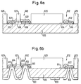
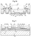
- Figures 6a-c are cross sectional elevation veiws of steps in preferred embodiment of fabrication including backside passive components.
- Figure 7 is a cross sectional elevation view showing frontside passive components.
- FIG. 3 heuristically shows in cross sectional elevation view first preferred embodiment monolithic microwave integrated circuit (MMIC) 300 wire bonded to lead 332 on alumina substrate 330 and with ground plane 306 attached to heat sink 320.
- MMIC 300 includes MESFET 304 with ground plane 306 also forming the air bridge on the source contacts of MESFET 304.
- the drain and gate of MESFET 304 connect through metallized vias such as 314 to backside input/ouput pad 312 and wire bond 310.
- the backside also contains microstrip 308.
- MMIC 300 combines the wire bonding of MMIC 100 of Figure 1 and the direct thermal contact to the source air bridge of flip-chip MMIC 200.
- MMIC 300 provides a frontside ground plane for direct overall contact on the frontside and consequent overall heat sinking and avoids the heat sink substrate patterning and alignment required for a flip-chip as MMIC 200 of Figure 2.
- the frontside ground plane demands backside microstrip lines and input/output pads, but these may be easily fabricated by just patterning what would have been a backside ground plane.
- MMIC 300 provides a more extensive frontside heat sinking than a flip-chip MMIC 200 without the alignment of patterned pads of such a flip-chip.
- MMIC 300 and similar other MMICs and discrete devices may be fabricated with simple processing steps after standard frontside processing for both MESFETs and HBTs.
- a first preferred embodiment method of fabrication creates a discrete multifinger heterojunction bipolar transistor (HBT) with frontside ground plane and includes the following steps as illustrated in cross sectional elevation and plan views in Figures 4a-r.
- HBT discrete multifinger heterojunction bipolar transistor
- the Figures illustrate an HBT with only two emitter fingers, four base contact fingers, and three collector contact fingers.
- high power microwave HBTs would have many more emitter, gate, and collector fingers.
- (1) Begin with 625-mm-thick (100)-oriented semi-insulating GaAs wafer 450. Epitaxially grow by metalorganic molecular beam epitaxy (MOMBE) or metalorganic chemical vapor deposition (MOCVD) the layers listed in Table I on wafer 450.
- MOMBE metalorganic molecular beam epitaxy
- MOCVD metalorganic chemical vapor deposition
- MOMBE elemental Ga and Al sources provide the group-III species
- tertiarybutlyarsine and tertiarybutylphosphine provide the group-V species after cracking.
- Elemental tin provides the n type doping
- elemental beryllium provides the p type doping.
- MOCVD use trimethylgallium, trimethylaluminum and tertiarybutylarsine with disilane providing silicon for the n type doping and carbon tetrachloride providing carbon for the p type doping.
- Table I Layer Material Thickness Doping Level (x1017/cm3) Cap n+ GaAs 200 nm 15 Grading n Al x Ga 1-x As 100 nm 5 Emitter n Al 0.35 Ga 0.65 As 100 nm 2 Spacer n+ GaAs 6 nm 10 Base p++ GaAs 80 nm 300 Collector n- GaAs 1000 nm 0.1 Subcollector n+ GaAs 1500 nm 10 Note that x varies from 0 to 0.35, that the total thickness of these doped layers is only roughly 3 mm, and that all of the individual layers do not appear in the Figures.
- the metal includes three sublayers: first germanium (Ge), then nickel (Ni), and lastly gold (Au) for a bondable or platable surface. The metal has a total thickness of about 290 nm.
- etching 400 nm may be performed without difficulty.
- the etch rate can be widely varied by varying the concentration of the ingredients. In particular, a mixture with volume ratios of acid (concentrated) to peroxide to water of 1 to 8 to 160 etches at roughly 300 nm/minute, whereas with ratio 3 to 1 to 1 will etch at roughly 2000 nm/minute.
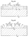
- the emitter regions each has dimensions of 2 mm by 30 mm, so even with an isotropic wet etch, the etch does not overly undercut emitter contacts 402. See Figure 4a for a plan view including one die area in a wafer and Figure 4b for a cross sectional elevation view along line b-b of Figure 4a. Note that the active area is indicated by a broken line Figure 4a and that the vertical scale in Figure 4b (and also all in other cross sectional elevatino view Figures) is exaggerated for clarity.
- (4) Spin on photoresist and pattern it to define the location of base contacts 408, evaporate and liftoff metal (290 nm of Ti/Pt/Au) base contact 408.
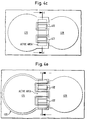
- Base contact 408 includes fingers adjacent the emitter contacts 402 and each has dimensions of 1 mm by 30 mm. Then, spin on photoresist and pattern it to define the collector contact recess 420. Using the patterned photoresist as an etch mask, perform a sulfuric acid/peroxide etch through GaAs base layer 406 and grading layers plus collector layer 410 and stop in n++ GaAs subcollector layer 412. See plan view Figure 4c and cross sectional elevation veiw Figure 4d with the section being along line d-d of Figure 4c. Note that the patterned photeresist is not shown in Figures 4c-d but remains on for the next step.
- collector contact recess 420 Using the patterned photoresist from step (4) for etching collector contact recess 420, evaporate and liftoff metal (290 nm of Ge/Ni/Au) to form collector contacts 414.
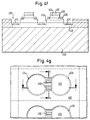
- the collector contact has fingers adjacent the base contact fingers, and each collector contact finger has dimensions of 2 mm by 30 mm. Note that the wet etch of collector contact recess 420 undercuts the patterned photoresist, and thus collector contact 414 will be spaced slightly from the edge of recess 420. Strip the patterned photoresist. This completes the HBT devices on the frontside of wafer 450 as shown in plan view by Figure 4e and in cross sectional elevation view in Figure 4f with the section along line f-f of Figure 4e.
- Base contact 408 and collector contact 414 are both thickened in the portions away from the base and collector contact fingers by liftoff of 500 nm of Ti/Cr/Pt/Au.
- the chromium will act as an etchstop in the via etch step infra .
- (6) Deposit by chemical vapor deposition silicon nitride (Si3N4) 455 to a thickness of 200 nm over the entire frontside of wafer 450.
- the nitride deposits conformally and acts as a passivant and a protective layer for the wafer. Then spin on photoresist and pattern it to define the location for first level metal on wafer 450.
- First level metal will cover all portions of wafer 450 away from the HBT (including the base and collector contacts) plus will cover the emitter contacts.
- reactive ion etch nitride 455 with the patterned photoresist as etch mask and then evaporate first level metal (290 nm of Ti/Pt/Au) 460 and liftoff the patterned photoresist (plus metal) by dissolution in acetone.
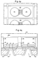
- Figure 4g for a plan view and Figures 4h-i for the cross sectional elevation views along lines h-h and i-i, respectively, of Figure 4g.
- the plated surface is roughly planar with the highest points at the air bridges 476; this insures that good thermal contact at the air bridges will be made with the heat sink eventually pressed against the ground plane for flip-chip mounting.
- (10) Mount wafer 450 with frontside ground plane gold plate 488 down on quartz carrier 490 using a layer of wax; the greater height of gold 488 over air bridge 476 than over metal 478 implies thinner wax over the air bridge as suggested by the indentation in Figure 4q.
- thin wafer 450 to a thickness of about 100 mm from the backside.
- the two backside grounds 494 serve as the grounds for a coplanar waveguide with center lead bond pad 492 (connected to collector contact 414) and a coplanar waveguide with center lead bond pad 493 (connected to base contact 408).
- the alumina substrate 330 of Figure 3 would have coplanar waveguides on its upper surface for wirebonding to the waveguides with bond pads 492 and 493.
- Other preferred embodiments infra include items such as transmission lines and inductors and capacitor plates in this backside definition and plating.
- Each die may then be mounted with (frontside) gold 488 (and thus HBT emitter) down on a low-thermal-resistance baseplate, such as gold or diamond, using gold-tin solder or other such attachment methods.
- Electrical contacts to the bond pads 492 may be by ball bonding, as illustrated in Figure 3 by wire bond 310, and frontside ground plane 488 on a heat sink corresponds to ground plane 306 on heat sink 320 of Figure 3.
- Figure 4q appears upside down when compared to Figure 3. This completes the fabrication.
- Alternative fabrication embodiments include substitution of various steps such as uniform deposition or plating of metal followed by patterned photoresist and etching in place of the previously described selective plating using patterned photoresist or dielectric.
- step (6) cross sectional elevation view Figures 4h-i
- step (6) cross sectional elevation view Figures 4h-i
- step (6) sputter on a thin (50 nm) gold layer overall
- step (7) electroplate gold to form the frontside ground plane 588 (5-15 mm thick).
- step (10) and (11) sputter on a thin (50 nm) gold layer overall
- step (8) spin on photoresist and pattern it to expose all areas which will be in direct contact with the frontside ground plane 588.
- electroplate gold to form the frontside ground plane 588 (5-15 mm thick).
- strip the photoresist and exposed thin gold See Figures 5a-b.
- the two step ground plane plating has the advantage that the air bridge first plating is relatively thin and thus does not need thick patterned photoresist. Also, air bridge has relatively small area so the photoresists and thin metal 472 are easy to strip.
- the second step thick plating uses polyimide coverage and no (thick) photoresist for patternless plating with the areas plated being continuous.
- the HBTs may be isolated by a mesa etch down to the semi-insulating wafer; this would require a photoresist masking about the HBT prior to the first level metal step and an etch.
- the FETs would be then fabricated, and the preceding fabrication continued with first level metal.
- FET source/drains and channel regions may be implanted followed by source/drain ohmic metal liftoff and gate metal liftoff together with chromium layers added where vias from the backside would come through to thin metal.
- the FETs could use doped layers originally grown for or below the HBT layers or use an epitaxial overgrowth.
- MMICs with multiple HBTs and/or FETs may be made with the nongrounded emitter, base, collector, source, drain, and gate contacts connected by vias to the backside as described in the next section.
- a preferred embodiment frontside fabrication method may be combined with fabrication of passive components such as resistors, transmission lines (microstrip lines using the frontside ground plane or coplanar waveguides), inductors, interconnects, and bond pads and the backside and connected to the frontside devices by vias.
- a preferred embodiment method of fabrication includes the following steps.
- passive components such as resistors and capacitors may also be formed on the frontside.
- step (6) after the deposition of nitride 455 but prior to patterning and etching plus first level metal liftoff, spin on photoresist and pattern it to define locations for thin film resistors 702.
- step (6) after the deposition of nitride 455 but prior to patterning and etching plus first level metal liftoff, spin on photoresist and pattern it to define locations for thin film resistors 702.
- thin film resistor material such as tantalum nitride or nickel chromium and liftoff the patterned photoresist.
- FIG. 7 is analogoud to Figure 4l and shows one finger HBT 770 with resister 702 and capacitor 706-708. Vias to the backside may be made to interconnects for resistor 702 and capacitor plates 706 or 708 by including chromium etch stops in the metal.
- the preferred embodiments may be varied in many ways while retaining one or more of the features of a frontside ground plane with vias to backside contacts and passive components on backside or frontside or both.
- the dimensions and layouts of the devices may be varied.
- the semiconductor materials may be replaced with other III-V compounds such as InP, GaAsP, InGaAs, InAlGaAs, ..., or other semiconductors generally such as silicon, germanium, silicon-germanium alloys, II-VI compounds such as HgCdTe, or silicon carbide and diamond.
- Semiconductor-on-insulator substrates or bonded wafers may replace the semi-insulating wafer.
- the devices integrated may include homojunction bipolars, double heterojunction bipolars, junction FETs, thyristors, and so forth.
Landscapes
- Bipolar Transistors (AREA)
- Semiconductor Integrated Circuits (AREA)
- Junction Field-Effect Transistors (AREA)
Applications Claiming Priority (2)
| Application Number | Priority Date | Filing Date | Title |
|---|---|---|---|
| US08/159,648 US6028348A (en) | 1993-11-30 | 1993-11-30 | Low thermal impedance integrated circuit |
| US159648 | 1993-11-30 |
Publications (1)
| Publication Number | Publication Date |
|---|---|
| EP0663693A1 true EP0663693A1 (de) | 1995-07-19 |
Family
ID=22573407
Family Applications (1)
| Application Number | Title | Priority Date | Filing Date |
|---|---|---|---|
| EP19940118870 Withdrawn EP0663693A1 (de) | 1993-11-30 | 1994-11-30 | Integrierte Schaltung mit niedrigem Wärmewiderstand |
Country Status (4)
| Country | Link |
|---|---|
| US (2) | US6028348A (de) |
| EP (1) | EP0663693A1 (de) |
| JP (1) | JPH088272A (de) |
| KR (1) | KR950015757A (de) |
Cited By (10)
| Publication number | Priority date | Publication date | Assignee | Title |
|---|---|---|---|---|
| EP0703614A3 (de) * | 1994-08-31 | 1997-03-12 | Texas Instruments Inc | Flip-Chip mit wärmeableitender Lage |
| WO1997021246A1 (en) * | 1995-12-08 | 1997-06-12 | The Whitaker Corporation | Heterolithic microwave integrated impedance matching circuitry and method of manufacture |
| WO2001078120A1 (en) * | 2000-04-11 | 2001-10-18 | Cree, Inc. | Method of forming vias in silicon carbide and resulting devices and circuits |
| FR2832855A1 (fr) * | 2001-11-27 | 2003-05-30 | St Microelectronics Sa | Circuit monolithique double face |
| EP1564806A1 (de) * | 2004-02-17 | 2005-08-17 | Sanyo Electric Co., Ltd. | Halbleiterbauelement und Methode zu seiner Herstellung |
| DE102004059884A1 (de) * | 2004-12-10 | 2006-06-29 | Forschungsverbund Berlin E.V. | Verfahren zur Flip-Chip-Montage von Mikrochips und damit hergestellte elektronische Baugruppe |
| US7125786B2 (en) | 2000-04-11 | 2006-10-24 | Cree, Inc. | Method of forming vias in silicon carbide and resulting devices and circuits |
| US7892974B2 (en) | 2000-04-11 | 2011-02-22 | Cree, Inc. | Method of forming vias in silicon carbide and resulting devices and circuits |
| EP1490903B1 (de) * | 2002-03-26 | 2015-02-25 | Intel Corporation | Halbleitervorrichtung mit bauelementen, die in einer diamantschichtauf der rückseite der vorrichtung eingebettet sind |
| TWI793753B (zh) * | 2020-11-18 | 2023-02-21 | 日商村田製作所股份有限公司 | 半導體裝置 |
Families Citing this family (60)
| Publication number | Priority date | Publication date | Assignee | Title |
|---|---|---|---|---|
| US6048777A (en) * | 1997-12-18 | 2000-04-11 | Hughes Electronics Corporation | Fabrication of high power semiconductor devices with respective heat sinks for integration with planar microstrip circuitry |
| US6001723A (en) * | 1997-12-24 | 1999-12-14 | National Semiconductor Corporation | Application of wire bond loop as integrated circuit package component interconnect |
| FR2784230B1 (fr) * | 1998-10-05 | 2000-12-29 | St Microelectronics Sa | Procede de realisation d'un isolement inter et/ou intra-metallique par air dans un circuit integre et circuit integre obtenu |
| SE515661C2 (sv) * | 1998-12-22 | 2001-09-17 | Ericsson Telefon Ab L M | Trådbondningskompensering |
| US6194774B1 (en) * | 1999-03-10 | 2001-02-27 | Samsung Electronics Co., Ltd. | Inductor including bonding wires |
| US6403144B1 (en) | 1999-04-30 | 2002-06-11 | The Procter & Gamble Co. | Food preparation compositions |
| JP2000349096A (ja) * | 1999-06-01 | 2000-12-15 | Matsushita Electric Ind Co Ltd | 化合物電界効果トランジスタおよびその製造方法 |
| US7335965B2 (en) * | 1999-08-25 | 2008-02-26 | Micron Technology, Inc. | Packaging of electronic chips with air-bridge structures |
| US7276788B1 (en) | 1999-08-25 | 2007-10-02 | Micron Technology, Inc. | Hydrophobic foamed insulators for high density circuits |
| US6798061B2 (en) * | 1999-11-15 | 2004-09-28 | Koninklijke Philips Electronics N.V. | Multiple semiconductor chip (multi-chip) module for use in power applications |
| US6890847B1 (en) * | 2000-02-22 | 2005-05-10 | Micron Technology, Inc. | Polynorbornene foam insulation for integrated circuits |
| US6759746B1 (en) * | 2000-03-17 | 2004-07-06 | Robert Bruce Davies | Die attachment and method |
| US6368929B1 (en) | 2000-08-17 | 2002-04-09 | Motorola, Inc. | Method of manufacturing a semiconductor component and semiconductor component thereof |
| JP4089143B2 (ja) * | 2000-08-30 | 2008-05-28 | 三菱電機株式会社 | 電力用半導体装置 |
| US6580107B2 (en) * | 2000-10-10 | 2003-06-17 | Sanyo Electric Co., Ltd. | Compound semiconductor device with depletion layer stop region |
| KR100385225B1 (ko) * | 2001-03-23 | 2003-05-27 | 삼성전자주식회사 | 탐침 패드 및 범프 패드를 갖는 플립 칩형 반도체소자 및 그 제조방법 |
| US6724067B2 (en) * | 2001-04-13 | 2004-04-20 | Anadigics, Inc. | Low stress thermal and electrical interconnects for heterojunction bipolar transistors |
| US6649978B2 (en) * | 2001-06-19 | 2003-11-18 | Koninklijke Philips Electronics N.V. | Semiconductor module having multiple semiconductor chips |
| FR2827424B1 (fr) * | 2001-07-13 | 2005-02-18 | Thales Sa | Composant electronique encapsule comportant un dispositif electronique de puissance et procede de fabrication |
| US6803667B2 (en) * | 2001-08-09 | 2004-10-12 | Denso Corporation | Semiconductor device having a protective film |
| EP1423878A2 (de) * | 2001-08-29 | 2004-06-02 | Koninklijke Philips Electronics N.V. | Integrierte schaltung mit löthöckernbrücken und verfahren zur deren herstellung |
| FR2830683A1 (fr) | 2001-10-10 | 2003-04-11 | St Microelectronics Sa | Realisation d'inductance et de via dans un circuit monolithique |
| US6849879B2 (en) * | 2001-10-15 | 2005-02-01 | Teraburst Networks, Inc. | Crosstalk reduction in a crosspoint thyristor switching array using a shielded dielectric stack |
| US20030095014A1 (en) * | 2001-11-21 | 2003-05-22 | Lao Binneg Y. | Connection package for high-speed integrated circuit |
| US6803252B2 (en) * | 2001-11-21 | 2004-10-12 | Sierra Monolithics, Inc. | Single and multiple layer packaging of high-speed/high-density ICs |
| JP3674780B2 (ja) * | 2001-11-29 | 2005-07-20 | ユーディナデバイス株式会社 | 高周波半導体装置 |
| US6830959B2 (en) * | 2002-01-22 | 2004-12-14 | Fairchild Semiconductor Corporation | Semiconductor die package with semiconductor die having side electrical connection |
| US20050077540A1 (en) * | 2002-01-25 | 2005-04-14 | Axel Hulsmann | Integrated circuit arrangement |
| US6737931B2 (en) * | 2002-07-19 | 2004-05-18 | Agilent Technologies, Inc. | Device interconnects and methods of making the same |
| JP2005158800A (ja) * | 2003-11-20 | 2005-06-16 | Sharp Corp | 半導体装置の製造方法及びその製造方法により製造された半導体装置 |
| US7194711B2 (en) * | 2004-01-28 | 2007-03-20 | Gradient Design Automation Inc. | Method and apparatus for full-chip thermal analysis of semiconductor chip designs |
| US7353471B1 (en) * | 2004-08-05 | 2008-04-01 | Gradient Design Automation Inc. | Method and apparatus for using full-chip thermal analysis of semiconductor chip designs to compute thermal conductance |
| US20090077508A1 (en) * | 2004-01-28 | 2009-03-19 | Rubin Daniel I | Accelerated life testing of semiconductor chips |
| US7203920B2 (en) * | 2004-01-28 | 2007-04-10 | Gradient Design Automation Inc. | Method and apparatus for retrofitting semiconductor chip performance analysis tools with full-chip thermal analysis capabilities |
| US20090224356A1 (en) * | 2004-01-28 | 2009-09-10 | Rajit Chandra | Method and apparatus for thermally aware design improvement |
| US7458052B1 (en) | 2004-08-30 | 2008-11-25 | Gradient Design Automation, Inc. | Method and apparatus for normalizing thermal gradients over semiconductor chip designs |
| US20090048801A1 (en) * | 2004-01-28 | 2009-02-19 | Rajit Chandra | Method and apparatus for generating thermal test vectors |
| US7383520B2 (en) * | 2004-08-05 | 2008-06-03 | Gradient Design Automation Inc. | Method and apparatus for optimizing thermal management system performance using full-chip thermal analysis of semiconductor chip designs |
| US7472363B1 (en) * | 2004-01-28 | 2008-12-30 | Gradient Design Automation Inc. | Semiconductor chip design having thermal awareness across multiple sub-system domains |
| US7401304B2 (en) * | 2004-01-28 | 2008-07-15 | Gradient Design Automation Inc. | Method and apparatus for thermal modeling and analysis of semiconductor chip designs |
| US8019580B1 (en) | 2007-04-12 | 2011-09-13 | Gradient Design Automation Inc. | Transient thermal analysis |
| US8286111B2 (en) * | 2004-03-11 | 2012-10-09 | Gradient Design Automation Inc. | Thermal simulation using adaptive 3D and hierarchical grid mechanisms |
| US7109587B1 (en) * | 2004-05-25 | 2006-09-19 | National Semiconductor Corporation | Apparatus and method for enhanced thermal conductivity packages for high powered semiconductor devices |
| US7202562B2 (en) | 2004-12-02 | 2007-04-10 | Micron Technology, Inc. | Integrated circuit cooling system and method |
| JP2006216883A (ja) * | 2005-02-07 | 2006-08-17 | Matsushita Electric Ind Co Ltd | 半導体集積回路装置 |
| JP4745007B2 (ja) * | 2005-09-29 | 2011-08-10 | 三洋電機株式会社 | 半導体装置及びその製造方法 |
| EP1960921A1 (de) * | 2005-12-17 | 2008-08-27 | Gradient Design Automation, Inc. | Simulation von ic-temperaturverteilungen über ein adaptives 3d-gitter |
| US7563714B2 (en) * | 2006-01-13 | 2009-07-21 | International Business Machines Corporation | Low resistance and inductance backside through vias and methods of fabricating same |
| US7919855B2 (en) * | 2006-02-21 | 2011-04-05 | Lockheed Martin | Topside thermal management of semiconductor devices using boron phosphide contacting a gate terminal |
| US8143654B1 (en) * | 2008-01-16 | 2012-03-27 | Triquint Semiconductor, Inc. | Monolithic microwave integrated circuit with diamond layer |
| US7884394B2 (en) * | 2009-02-09 | 2011-02-08 | Transphorm Inc. | III-nitride devices and circuits |
| US20110222757A1 (en) | 2010-03-10 | 2011-09-15 | Gbo 3D Technology Pte. Ltd. | Systems and methods for 2D image and spatial data capture for 3D stereo imaging |
| US20130265733A1 (en) * | 2012-04-04 | 2013-10-10 | Texas Instruments Incorporated | Interchip communication using an embedded dielectric waveguide |
| US9323870B2 (en) | 2012-05-01 | 2016-04-26 | Advanced Micro Devices, Inc. | Method and apparatus for improved integrated circuit temperature evaluation and IC design |
| CN103311180B (zh) * | 2013-05-17 | 2016-06-29 | 中国电子科技集团公司第十三研究所 | 一种改善mmic功率放大器性能的芯片布局方法 |
| JP2016006870A (ja) | 2014-05-30 | 2016-01-14 | 住友電気工業株式会社 | 半導体装置 |
| US10236239B2 (en) * | 2015-01-29 | 2019-03-19 | Avago Technologies International Sales Pte. Limited | Apparatus and semiconductor structure including a multilayer package substrate |
| TWI575683B (zh) * | 2015-11-19 | 2017-03-21 | 南茂科技股份有限公司 | 晶片封裝結構與其製作方法 |
| JP7046212B2 (ja) | 2018-03-14 | 2022-04-01 | エンベリオン オイ | 表面mesfet |
| US11167983B2 (en) * | 2019-01-14 | 2021-11-09 | Texas Instruments Incorporated | Selective wafer removal process for wafer bonding applications |
Citations (4)
| Publication number | Priority date | Publication date | Assignee | Title |
|---|---|---|---|---|
| US4794093A (en) * | 1987-05-01 | 1988-12-27 | Raytheon Company | Selective backside plating of gaas monolithic microwave integrated circuits |
| US4992764A (en) * | 1989-02-21 | 1991-02-12 | Hittite Microwave Corporation | High-power FET circuit |
| EP0446125A1 (de) * | 1990-03-09 | 1991-09-11 | Thomson-Csf Semiconducteurs Specifiques | Leistungshalbleiteranordnung |
| US5084750A (en) * | 1991-02-20 | 1992-01-28 | Raytheon Company | Push-pull heterojunction bipolar transistor |
Family Cites Families (2)
| Publication number | Priority date | Publication date | Assignee | Title |
|---|---|---|---|---|
| US5023993A (en) * | 1988-09-30 | 1991-06-18 | Grumman Aerospace Corporation | Method for manufacturing a high-performance package for monolithic microwave integrated circuits |
| US5202752A (en) * | 1990-05-16 | 1993-04-13 | Nec Corporation | Monolithic integrated circuit device |
-
1993
- 1993-11-30 US US08/159,648 patent/US6028348A/en not_active Expired - Lifetime
-
1994
- 1994-11-30 JP JP33200294A patent/JPH088272A/ja active Pending
- 1994-11-30 KR KR1019940032731A patent/KR950015757A/ko not_active Ceased
- 1994-11-30 EP EP19940118870 patent/EP0663693A1/de not_active Withdrawn
-
1995
- 1995-06-07 US US08/476,832 patent/US5710068A/en not_active Expired - Lifetime
Patent Citations (4)
| Publication number | Priority date | Publication date | Assignee | Title |
|---|---|---|---|---|
| US4794093A (en) * | 1987-05-01 | 1988-12-27 | Raytheon Company | Selective backside plating of gaas monolithic microwave integrated circuits |
| US4992764A (en) * | 1989-02-21 | 1991-02-12 | Hittite Microwave Corporation | High-power FET circuit |
| EP0446125A1 (de) * | 1990-03-09 | 1991-09-11 | Thomson-Csf Semiconducteurs Specifiques | Leistungshalbleiteranordnung |
| US5084750A (en) * | 1991-02-20 | 1992-01-28 | Raytheon Company | Push-pull heterojunction bipolar transistor |
Cited By (21)
| Publication number | Priority date | Publication date | Assignee | Title |
|---|---|---|---|---|
| EP0703614A3 (de) * | 1994-08-31 | 1997-03-12 | Texas Instruments Inc | Flip-Chip mit wärmeableitender Lage |
| US5717231A (en) * | 1994-08-31 | 1998-02-10 | Texas Instruments Incorporated | Antenna having elements with improved thermal impedance |
| WO1997021246A1 (en) * | 1995-12-08 | 1997-06-12 | The Whitaker Corporation | Heterolithic microwave integrated impedance matching circuitry and method of manufacture |
| US7892974B2 (en) | 2000-04-11 | 2011-02-22 | Cree, Inc. | Method of forming vias in silicon carbide and resulting devices and circuits |
| US8202796B2 (en) | 2000-04-11 | 2012-06-19 | Cree, Inc. | Method of forming vias in silicon carbide and resulting devices and circuits |
| US6515303B2 (en) | 2000-04-11 | 2003-02-04 | Cree, Inc. | Method of forming vias in silicon carbide and resulting devices and circuits |
| US6649497B2 (en) | 2000-04-11 | 2003-11-18 | Cree, Inc. | Method of forming vias in silicon carbide and resulting devices and circuits |
| US6475889B1 (en) | 2000-04-11 | 2002-11-05 | Cree, Inc. | Method of forming vias in silicon carbide and resulting devices and circuits |
| US6946739B2 (en) | 2000-04-11 | 2005-09-20 | Cree, Inc. | Layered semiconductor devices with conductive vias |
| US10367074B2 (en) | 2000-04-11 | 2019-07-30 | Cree, Inc. | Method of forming vias in silicon carbide and resulting devices and circuits |
| US7125786B2 (en) | 2000-04-11 | 2006-10-24 | Cree, Inc. | Method of forming vias in silicon carbide and resulting devices and circuits |
| US9490169B2 (en) | 2000-04-11 | 2016-11-08 | Cree, Inc. | Method of forming vias in silicon carbide and resulting devices and circuits |
| EP2182548A3 (de) * | 2000-04-11 | 2010-08-11 | Cree, Inc. | Gruppe III-V Halbleitervorrichtung auf SiC Substrat |
| WO2001078120A1 (en) * | 2000-04-11 | 2001-10-18 | Cree, Inc. | Method of forming vias in silicon carbide and resulting devices and circuits |
| FR2832855A1 (fr) * | 2001-11-27 | 2003-05-30 | St Microelectronics Sa | Circuit monolithique double face |
| EP1490903B1 (de) * | 2002-03-26 | 2015-02-25 | Intel Corporation | Halbleitervorrichtung mit bauelementen, die in einer diamantschichtauf der rückseite der vorrichtung eingebettet sind |
| EP1564806A1 (de) * | 2004-02-17 | 2005-08-17 | Sanyo Electric Co., Ltd. | Halbleiterbauelement und Methode zu seiner Herstellung |
| US7759247B2 (en) | 2004-02-17 | 2010-07-20 | Sanyo Electric Co., Ltd. | Manufacturing method of semiconductor device with a barrier layer and a metal layer |
| US7256497B2 (en) | 2004-02-17 | 2007-08-14 | Sanyo Electric Co., Ltd. | Semiconductor device with a barrier layer and a metal layer |
| DE102004059884A1 (de) * | 2004-12-10 | 2006-06-29 | Forschungsverbund Berlin E.V. | Verfahren zur Flip-Chip-Montage von Mikrochips und damit hergestellte elektronische Baugruppe |
| TWI793753B (zh) * | 2020-11-18 | 2023-02-21 | 日商村田製作所股份有限公司 | 半導體裝置 |
Also Published As
| Publication number | Publication date |
|---|---|
| US5710068A (en) | 1998-01-20 |
| KR950015757A (ko) | 1995-06-17 |
| US6028348A (en) | 2000-02-22 |
| JPH088272A (ja) | 1996-01-12 |
Similar Documents
| Publication | Publication Date | Title |
|---|---|---|
| US5710068A (en) | Low thermal impedance integrated circuit | |
| US11837457B2 (en) | Packaging for RF transistor amplifiers | |
| US3986196A (en) | Through-substrate source contact for microwave FET | |
| US5949140A (en) | Microwave semiconductor device with via holes and associated structure | |
| US5449930A (en) | High power, compound semiconductor device and fabrication process | |
| US5578841A (en) | Vertical MOSFET device having frontside and backside contacts | |
| US20090194792A1 (en) | Semiconductor device and manufacturing method therefor | |
| US12015004B2 (en) | Hybrid device assemblies and method of fabrication | |
| US6940157B2 (en) | High frequency semiconductor module, high frequency semiconductor device and manufacturing method for the same | |
| US12581728B2 (en) | Microwave integrated circuits including gallium-nitride devices on silicon | |
| US4298879A (en) | Field effect transistor | |
| JP4492034B2 (ja) | Hemt及びその製造方法 | |
| US5831337A (en) | Vertical-type transistor device, having a bump electrode that has a shape with no interior angle exceeding 270° | |
| US20030178655A1 (en) | Dual sided power amplifier | |
| US20240105692A1 (en) | Packaged flip chip radio frequency transistor amplifier circuits | |
| US5436497A (en) | Semiconductor device having a plurality of vertical type transistors having non-intersecting interconnections | |
| US5683919A (en) | Transistor and circuit incorporating same | |
| US4374394A (en) | Monolithic integrated circuit | |
| US4238763A (en) | Solid state microwave devices with small active contact and large passive contact | |
| JP2006114732A (ja) | 半導体装置及びその製造方法、並びに半導体モジュール | |
| JP2001093914A (ja) | 半導体能動素子及び半導体集積回路 | |
| JP3264517B2 (ja) | 縦型構造へテロ接合バイポーラトランジスタ | |
| JP3674881B2 (ja) | 半導体装置 | |
| JP3268064B2 (ja) | 半導体装置 | |
| JP3229185B2 (ja) | 半導体チップ、その製造方法、半導体素子、および半導体装置 |
Legal Events
| Date | Code | Title | Description |
|---|---|---|---|
| PUAI | Public reference made under article 153(3) epc to a published international application that has entered the european phase |
Free format text: ORIGINAL CODE: 0009012 |
|
| AK | Designated contracting states |
Kind code of ref document: A1 Designated state(s): DE FR GB IT NL |
|
| 17P | Request for examination filed |
Effective date: 19960103 |
|
| 17Q | First examination report despatched |
Effective date: 19970728 |
|
| STAA | Information on the status of an ep patent application or granted ep patent |
Free format text: STATUS: THE APPLICATION IS DEEMED TO BE WITHDRAWN |
|
| 18D | Application deemed to be withdrawn |
Effective date: 19980210 |