EP0664569B1 - Mikroelektronisches Bauelement - Google Patents
Mikroelektronisches Bauelement Download PDFInfo
- Publication number
- EP0664569B1 EP0664569B1 EP95100274A EP95100274A EP0664569B1 EP 0664569 B1 EP0664569 B1 EP 0664569B1 EP 95100274 A EP95100274 A EP 95100274A EP 95100274 A EP95100274 A EP 95100274A EP 0664569 B1 EP0664569 B1 EP 0664569B1
- Authority
- EP
- European Patent Office
- Prior art keywords
- individual elements
- layer structure
- contact structures
- substrate
- component according
- Prior art date
- Legal status (The legal status is an assumption and is not a legal conclusion. Google has not performed a legal analysis and makes no representation as to the accuracy of the status listed.)
- Expired - Lifetime
Links
Images


Classifications
-
- B—PERFORMING OPERATIONS; TRANSPORTING
- B82—NANOTECHNOLOGY
- B82Y—SPECIFIC USES OR APPLICATIONS OF NANOSTRUCTURES; MEASUREMENT OR ANALYSIS OF NANOSTRUCTURES; MANUFACTURE OR TREATMENT OF NANOSTRUCTURES
- B82Y10/00—Nanotechnology for information processing, storage or transmission, e.g. quantum computing or single electron logic
-
- H—ELECTRICITY
- H10—SEMICONDUCTOR DEVICES; ELECTRIC SOLID-STATE DEVICES NOT OTHERWISE PROVIDED FOR
- H10K—ORGANIC ELECTRIC SOLID-STATE DEVICES
- H10K10/00—Organic devices specially adapted for rectifying, amplifying, oscillating or switching; Organic capacitors or resistors having potential barriers
- H10K10/40—Organic transistors
- H10K10/46—Field-effect transistors, e.g. organic thin-film transistors [OTFT]
- H10K10/462—Insulated gate field-effect transistors [IGFETs]
- H10K10/466—Lateral bottom-gate IGFETs comprising only a single gate
-
- H—ELECTRICITY
- H10—SEMICONDUCTOR DEVICES; ELECTRIC SOLID-STATE DEVICES NOT OTHERWISE PROVIDED FOR
- H10K—ORGANIC ELECTRIC SOLID-STATE DEVICES
- H10K85/00—Organic materials used in the body or electrodes of devices covered by this subclass
- H10K85/20—Carbon compounds, e.g. carbon nanotubes or fullerenes
- H10K85/211—Fullerenes, e.g. C60
-
- H—ELECTRICITY
- H10—SEMICONDUCTOR DEVICES; ELECTRIC SOLID-STATE DEVICES NOT OTHERWISE PROVIDED FOR
- H10N—ELECTRIC SOLID-STATE DEVICES NOT OTHERWISE PROVIDED FOR
- H10N70/00—Solid-state devices having no potential barriers, and specially adapted for rectifying, amplifying, oscillating or switching
-
- H—ELECTRICITY
- H10—SEMICONDUCTOR DEVICES; ELECTRIC SOLID-STATE DEVICES NOT OTHERWISE PROVIDED FOR
- H10D—INORGANIC ELECTRIC SEMICONDUCTOR DEVICES
- H10D62/00—Semiconductor bodies, or regions thereof, of devices having potential barriers
- H10D62/80—Semiconductor bodies, or regions thereof, of devices having potential barriers characterised by the materials
- H10D62/83—Semiconductor bodies, or regions thereof, of devices having potential barriers characterised by the materials being Group IV materials, e.g. B-doped Si or undoped Ge
-
- Y—GENERAL TAGGING OF NEW TECHNOLOGICAL DEVELOPMENTS; GENERAL TAGGING OF CROSS-SECTIONAL TECHNOLOGIES SPANNING OVER SEVERAL SECTIONS OF THE IPC; TECHNICAL SUBJECTS COVERED BY FORMER USPC CROSS-REFERENCE ART COLLECTIONS [XRACs] AND DIGESTS
- Y10—TECHNICAL SUBJECTS COVERED BY FORMER USPC
- Y10T—TECHNICAL SUBJECTS COVERED BY FORMER US CLASSIFICATION
- Y10T428/00—Stock material or miscellaneous articles
- Y10T428/24—Structurally defined web or sheet [e.g., overall dimension, etc.]
- Y10T428/24802—Discontinuous or differential coating, impregnation or bond [e.g., artwork, printing, retouched photograph, etc.]
- Y10T428/24917—Discontinuous or differential coating, impregnation or bond [e.g., artwork, printing, retouched photograph, etc.] including metal layer
-
- Y—GENERAL TAGGING OF NEW TECHNOLOGICAL DEVELOPMENTS; GENERAL TAGGING OF CROSS-SECTIONAL TECHNOLOGIES SPANNING OVER SEVERAL SECTIONS OF THE IPC; TECHNICAL SUBJECTS COVERED BY FORMER USPC CROSS-REFERENCE ART COLLECTIONS [XRACs] AND DIGESTS
- Y10—TECHNICAL SUBJECTS COVERED BY FORMER USPC
- Y10T—TECHNICAL SUBJECTS COVERED BY FORMER US CLASSIFICATION
- Y10T428/00—Stock material or miscellaneous articles
- Y10T428/24—Structurally defined web or sheet [e.g., overall dimension, etc.]
- Y10T428/24802—Discontinuous or differential coating, impregnation or bond [e.g., artwork, printing, retouched photograph, etc.]
- Y10T428/24926—Discontinuous or differential coating, impregnation or bond [e.g., artwork, printing, retouched photograph, etc.] including ceramic, glass, porcelain or quartz layer
Definitions
- Microelectronic components in which a quantum mechanical Effect is exploited gain in terms of development very fast electronic components with a high degree of integration in importance.
- the interest is directed among other things on the effect of the Coulomb blockade described in K.K. Likharev, Granular Nanoelectronics, D.K. Ferry ed., Plenum, N.Y. (1991) S. 371 ff. Is described.
- the Coulomb blockade is based on the effect that when an electron is tunneled through a tunnel contact, the energy of the entire system changes.
- Tunnel contact is understood to mean a structure which comprises two electrodes separated by an insulating layer, the insulating layer being so thin that individual electrons tunnel through the insulating layer.
- the energy change of the overall system is of the order of q 2 / e / C, where q e is the charge of an electron and C is the capacitance of the tunnel contact. If this change in energy is an increase in energy significantly above the thermal energy of the system k B T, where k B is the Boltzmann constant and T is the absolute temperature, the electron does not tunnel through the tunnel contact. This blocks the current through the tunnel contact. If, on the other hand, the energy change is of the order of magnitude or less than the thermal energy, i.e. q 2 / e / C ⁇ / ⁇ k B T, an electron may tunnel through the tunnel contact.
- two electrodes are used as a tunnel contact in the first case made of aluminum, between which a thin oxide layer is arranged (see A. Gladun et al, Physics in our Zeit, Vol. 23 (1992), pp. 159 ff.).
- a Coulomb blockade device is only functional at very low temperatures. The electrical properties of this tunnel contact by scaling the components.
- the Coulomb blockade effect at room temperature occurs only for elements with a tunnel contact with a capacity of Attofarad (10 -18 F) or below, according to the estimate of the energy change and thermal energy. Such elements have an expansion in the order of a few nanometers.
- Such small elements are contacted with the help of Scanning microscopes, such as the scanning tunnel microscope or the atomic force microscope (see C. Schönenberger et al, Europhys. Lett. Vol. 20 (1992) pp. 249 ff.). Other ways, elements of this size to contact are not known.
- Tunnel contact elements are used as tunnel contact elements in nanometer size have been proposed, surrounded by an insulating sheath are (see DE 42 12 220 A1).
- the electrical properties of this Tunnel contact elements are due to the size and type of the metal cluster as well as the insulating sheaths.
- DE 42 12 220 A1 describes the individual elements as a fill in an admission version to record and to contact accordingly via the admission version or a pressing body by pressing the individual elements to form under high pressure, which is provided with contacts.
- the component body as a disc with a 5 mm in diameter and 0.379 mm in thickness.
- Prefers are dimensions from 2 to 10 mm for the diameter and 0.1 to 1 mm for the thickness.
- Such components have a Threshold voltage on the order of kilo volts on what for use in microelectronics is unfavorable.
- the invention is based on the problem of a microelectronic Specify component that is scalable and can be produced lithographically is.
- a component is to be specified that is functional at room temperature.
- each individual element has an electrically conductive Covered area and an insulating layer opposite the electrically conductive area of the adjacent individual elements is isolated.
- the insulating layer is dimensioned so that the conductive areas of adjacent individual elements and those in between arranged insulating layer form a tunnel contact.
- structures are individual elements suitable, the one conductive core and one the conductive Insulating sheath surrounding core.
- the diameter of the The individual element is preferably between 1 and 10 nm.
- the capacity of the individual elements is so in this size range small that the component works in the room temperature range.
- metal clusters with organic are as individual elements Ligands as an insulating shell, as known from DE 42 12 220 A1, or fullerenes with enclosed metal core.
- the layer structure made of a porous semiconductor material preferably silicon form, which is so strongly etched that no continuous conductive There is more connection via the pores.
- conductive areas interact in such porous semiconductor materials grains of the semiconductor material located in the pores.
- porous semiconductor material is in particular porous silicon that formed by anodic etching in a fluoride-containing electrolyte becomes suitable.
- At least two contact structures are in the microelectronic component provided that electrically with the layer structure are connected.
- the two contact structures are preferably on arranged opposite sides of the layer structure.
- the Contact structures are thus on the main surface of the substrate arranged that individual elements located at the edge of the layer structure are in contact with the respective contact structure.
- Opposing contact structures are preferably at a distance between 20 and 500 nm. The perpendicular points to that Layer structure between 20 nm and 10 ⁇ m. Such dimensions are with the help of electron beam lithography or deep UV lithography can be produced.
- the contact structures are preferably made of doped polysilicon or formed from a metal.
- the layer structure and the contact structures are opposite to that Electrically insulated substrate.
- an insulating substrate Material such as glass or sapphire are used for Isolation no additional measures required. Is considered Silicon is used for the substrate, so the insulation is provided by insulating layer ensured, on the surface of the contact structures and the layer structures are arranged.
- the threshold voltage for the entire microelectronic component is 1.3 volts. This means that if a voltage of less than 1.3 volts is applied between the contact structures, the component blocks, whereas if a voltage of more than 1.3 volts is applied, the component conducts. This threshold voltage is of a magnitude that can reasonably be used for integrated circuits.
- a surface of the layer structure aligned parallel to the main surface of the substrate is to be provided with a gate dielectric.
- a gate electrode is arranged, which through the gate dielectric compared to the layer structure and the Contact structures is isolated.
- This embodiment of the invention microelectronic component provides a controllable Coulomb blockade device.
- the gate electrode on the substrate it is advantageous first the gate electrode on the substrate, then the gate dielectric and then the contact structures and the layer structure to apply.
- the contact structures and the layer structure are opposed in this case by the gate dielectric electrically isolated from the substrate. This way you can first the silicon process steps are carried out before the Contact structures the layer structure is deposited.
- the gate electrode in this Case as an implanted diffusion area in the surface of the To realize substrate.
- the Surface of the gate dielectric at least two gate electrodes arranged.
- Such an electron pump can be created by applying suitable AC voltages to the gate electrodes each have a specific one Amount of charge per period run through the arrangement. This can to generate a direct current whose magnitude depends on the frequency of the AC voltage is controlled.
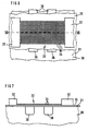
- a substrate 10 has a main surface 11 (see FIG. 1 and FIG. 2).
- the substrate 10 is insulating at least in the area of the main surface 11. It consists, for example, of silicon with an SiO 2 layer in the area of the main surface 11. Alternatively, the substrate consists of glass or sapphire.
- the contact structures 12 exist, for example made of doped polysilicon or a metal, preferably aluminum or titanium.
- the contact structures have parallel to the main surface 11 12 a width of 1 ⁇ m, for example.
- the contact structures 12 can be designed as part of supply lines or be contacted to the outside via a contact hole.
- Between the two contact structures 12 is one Layer structure 13 arranged.
- the layer structure 13 comprises individual elements, arranged as a single layer on the main surface 11 are. In the process, adjacent individual elements 14 touch among themselves. Individual elements 14 on the edge of the layer structure 13 are arranged and adjoin a contact structure 12, are in contact with the respective contact structure 12.
- Perpendicular to the connecting line between the contact structures 12 the layer structure has an extent of, for example, 1 ⁇ m on.
- the individual elements 14 are, for example, metal clusters with organic ones Ligands that form an insulating shell around the metal cluster form, fullerenes with enclosed metal core or porous Semiconductor material that is so strongly etched out that no through Conductive connection exists more and that the semiconductor material consists essentially of pores and semiconductor grains.
- 14 metal clusters are preferably used as a single element used an envelope of organic ligands, the metal cluster Contains 55 gold atoms.
- Such a single element 14 has a diameter of about 2 nm.
- the capacity between neighboring individual elements is about 0.2 aF.
- Adjacent individual elements 14 are connected to one another via a tunnel contact. If a voltage is applied between the contact structures 12 which is so great that the voltage drop across a single individual element 14 is less than the threshold voltage u th of a tunnel contact, then no current can flow through the layer structure 13. If, on the other hand, the voltage between the contact structures 12 is so great that the voltage drop across each individual element 14 is greater than the threshold voltage u th for the tunnel contact, electrons can tunnel through the tunnel contacts and current flows between the contact structures 12 through the layer structure 13 .
- FIG. 3 shows the current (I) -voltage (U) characteristic of the diode structure explained with reference to FIGS. 1 and 2.
- R T is the resistance of a tunnel contact and W is the extension of the contact structures 12 perpendicular to the distance between the contact structures 12.
- U th is, for example, 1.3 V
- R T is, for example, 100 k ⁇
- W is, for example, 1 ⁇ m
- L is Example 50 nm.U is given in units of the threshold voltage U th of the overall component.
- a substrate 20 includes a major surface 21 (see Figure 4 and Figure 5).
- the substrate 20 is insulating on the main surface 21.
- the substrate 20 is preferably made of silicon with an SiO 2 layer.
- the substrate 20 consists entirely of insulating material, for example glass or sapphire.
- the main surface 21 there are two contact structures 22, one Layer structure 23, which consists of a single-layer layer of individual elements 24 consists of a gate dielectric 25 and a gate electrode 26 arranged.
- the main electrode 21 is the gate electrode 26 arranged.
- the gate electrode 26 is, for example made of doped polysilicon or a metal, preferably Aluminum or titanium.
- the gate electrode 26 has a thickness from, for example, 50 nm.
- a gate dielectric 25 is arranged on the surface of the gate electrode 26.
- the gate dielectric 25 comprises, for example, SiO 2 and has a thickness of, for example, 10 nm.
- the contact structures 22 are on opposite sides of the Gate electrode 26 arranged.
- the contact structures preferably overlap 22 the edge of the gate dielectric 25.
- the contact structures 22 have a distance of, for example, 50 nm.
- the contact structures 22 have a parallel to the main surface 21 Width of 1 ⁇ m, for example.
- the thickness of the contact structures For example, 22 is 50 nm.
- the layer structure 23 is on the surface of the gate dielectric 25 arranged between the contact structures 22.
- the Layer structure 23 comprises the individual elements 24, which are in one layer are arranged. Adjacent individual elements touch each other 24. Individual elements 24 which are attached to the contact structures 22 adjacent sides of the layer structure 23 are arranged, touch the respective contact structure 22.
- the individual elements 24 are preferably metal clusters from 55 Gold atoms created by an envelope from an organic ligand are surrounded.
- the individual elements 24 can use other metal clusters with an organic ligand shell, fullerenes with enclosed metal core or porous semiconductor materials his.
- a substrate 30 has a main surface 31. On the main area 31, in addition to contact structures 32, a layer structure 33, which comprises individual elements 34 arranged in one layer, a gate dielectric 35 arranged.
- the substrate 30 comprises two gate electrodes 36, which adjoin the main surface 31.
- the substrate 30 is made of monocrystalline silicon, for example.
- the gate electrodes 36 are implanted as diffusion regions realized in the substrate 30 (see FIG. 6 and FIG. 7) and by pn junctions isolated from substrate 30.
- the gate dielectric 35 is arranged on the main surface 31. It covers the entire area for the component.
- the gate dielectric 35 comprises, for example, SiO 2 and has a thickness of, for example, 10 nm.
- the contact structures 32 exist for Example of doped polysilicon or a metal, preferably Aluminum or titanium.
- the contact structures 32 have one Thickness of, for example, 50 nm. Between the contact structures 32 there is a distance of, for example, 150 nm.
- the gate electrodes 36 are arranged in the substrate 30 so that they lie between the contact structures 32.
- the layer structure 33 is on the surface of the gate dielectric 35 arranged between the contact structures 33.
- the Layer structure 33 is formed from the individual elements 34 which arranged as a single-layer layer between the contact structures 32 are. Immediately adjacent individual elements touch each other 34. Those individual elements 34, which on one of the Contact structures 32 adjacent edge of the layer structure 33 are arranged, touch the contact structure 32.
- the individual elements 34 are preferably metal clusters with 55 Gold atoms created by an insulating organic ligand shell are surrounded.
- the insulating sleeves between adjacent metal clusters form a Coulomb barrier.
- the individual elements 34 have dimensions of approximately 2 nm.
- the individual elements Metal clusters of a different size may be of an insulating type Envelope are surrounded, or fullerenes with enclosed Metal core or made of porous semiconductor material.
- the contact structures 32 and the layer structure 33 are through the gate dielectric 35 is insulated from the substrate 30.
- the contact structure 32, the layer structure 33, the gate dielectric 35 and the two gate electrodes 36 form a component, in that by applying appropriate control voltages to the gate electrodes 36 charge clocked from one contact structure to the others can be moved. It is an electron pump following a principle similar to that described in C. Urbina et al, IEEE Trans. Magn. Vol. 27 (1991) pp. 2578 ff.
Landscapes
- Engineering & Computer Science (AREA)
- Chemical & Material Sciences (AREA)
- Nanotechnology (AREA)
- Materials Engineering (AREA)
- Physics & Mathematics (AREA)
- Mathematical Physics (AREA)
- Theoretical Computer Science (AREA)
- Crystallography & Structural Chemistry (AREA)
- Insulated Gate Type Field-Effect Transistor (AREA)
- Thin Film Transistor (AREA)
- Electrodes Of Semiconductors (AREA)
Description
- Figur 1
- stellt eine Aufsicht auf eine Diodenstruktur gemäß der Erfindung dar.
- Figur 2
- zeigt den in Figur 1 mit II-II bezeichneten Schnitt durch die Diodenstruktur.
- Figur 3
- zeigt die Kennlinie der in Figur 1 und Figur 2 dargestellten Diodenstruktur.
- Figur 4
- zeigt eine Aufsicht auf ein erfindungsgemäßes Bauelement mit einer Gateelektrode.
- Figur 5
- zeigt den in Figur 4 mit V-V bezeichneten Schnitt.
- Figur 6
- zeigt eine Aufsicht auf ein Bauelement mit zwei Gateelektroden, das als Drehtüranordnung einsetzbar ist.
- Figur 7
- zeigt den in Figur 6 mit VII-VII bezeichneten Schnitt.
Claims (8)
- Mikroelektronisches Bauelement,bei dem ein Substrat (10) mit einer Hauptfäche (11) vorgesehen ist,bei dem auf der Hauptfläche (11) des Substrats (10) eine Schichtstruktur (13) angeordnet ist, die in einer Lage nebeneinander angeordnete Einzelelemente (14) umfaßt,bei dem auf der Hauptfläche (11) des Substrats (10) mindestens zwei Kontaktstrukturen (12) vorgesehen sind, die mit der Schichtstruktur (13) elektrisch verbunden sind.bei dem die Einzelelemente (14) und die Kontaktstrukturen (12) gegenüber dem Substrat (10) elektrisch isoliert sind,bei dem die Einzelelemente untereinander jeweils über quantenmechanische Tunnelkontakte elektrisch verbunden sind,bei dem der Durchmesser der Einzelelemente zwischen 1 und 10 nm liegt.
- Bauelement nach Anspruch 1,bei dem jedes Einzelelement (14) einen leitfähigen Kern und eine den leitfähigen Kern umgebende isolierende Hülle umfaßt,bei dem der leitfähige Kern und die isolierende Hülle gemeinsam einen Durchmesser zwischen und 10 nm aufweisen,bei dem benachbarte Einzelelemente (14) so angeordnet sind, daß sich ihre isolierenden Hüllen berühren.
- Bauelement nach Anspruch 2,bei dem jedes Einzelelement (14) ein Metallcluster mit organischen Liganden als isolierender Hülle oder ein Fulleren mit eingeschlossenem Metallkern umfaßt.
- Bauelement nach Anspruch 1,bei dem die Einzelelemente (14) durch poröses Halbleitermaterial gebildet werden, das so stark ausgeätzt ist, daß keine durchgehende leitfähige Verbindung mehr besteht und bei dem die Einzelelemente (14) jeweils Abmessungen im Bereich zwischen 1 nm und 10 nm aufweisen.
- Bauelement nach einem der Ansprüche 1 bis 4,bei dem die Kontaktstrukturen (12) an gegenüberliegenden Seiten der Schichtstruktur (13) angeordnet sind.
- Bauelement nach Anspruch 5,bei dem die Schichtstruktur (13) parallel zum Abstand der Kontaktstrukturen (12) eine Ausdehnung zwischen 20 nm und 500 nm und senkrecht dazu eine Ausdehnung zwischen 20 nm und 10 µm aufweist.
- Bauelement nach Anspruch 5 oder 6,bei dem eine Oberfläche der Schichtstruktur (23, 33), die parallel zur Hauptfläche (21, 31) des Substrats (20, 30) ausgerichtet ist, mit einem Gatedielektrikum (25, 35) versehen ist,bei dem auf der Oberfläche des Gatedielektrikums (25, 35) auf der von der Schichtstruktur (23, 33) abgewandten Seite mindestens eine Gateelektrode (26, 36) angeordnet ist.
- Bauelement nach Anspruch 7,bei dem auf der Oberfläche des Gatedielektrikums (35) mindestens zwei Gateelektroden (36) angeordnet sind.
Applications Claiming Priority (2)
| Application Number | Priority Date | Filing Date | Title |
|---|---|---|---|
| DE4401442A DE4401442C1 (de) | 1994-01-19 | 1994-01-19 | Mikroelektronisches Bauelement |
| DE4401442 | 1994-01-19 |
Publications (2)
| Publication Number | Publication Date |
|---|---|
| EP0664569A1 EP0664569A1 (de) | 1995-07-26 |
| EP0664569B1 true EP0664569B1 (de) | 2000-05-10 |
Family
ID=6508232
Family Applications (1)
| Application Number | Title | Priority Date | Filing Date |
|---|---|---|---|
| EP95100274A Expired - Lifetime EP0664569B1 (de) | 1994-01-19 | 1995-01-10 | Mikroelektronisches Bauelement |
Country Status (4)
| Country | Link |
|---|---|
| US (1) | US5540977A (de) |
| EP (1) | EP0664569B1 (de) |
| JP (1) | JP3852963B2 (de) |
| DE (2) | DE4401442C1 (de) |
Families Citing this family (9)
| Publication number | Priority date | Publication date | Assignee | Title |
|---|---|---|---|---|
| US6783589B2 (en) * | 2001-01-19 | 2004-08-31 | Chevron U.S.A. Inc. | Diamondoid-containing materials in microelectronics |
| US7273598B2 (en) * | 2001-01-19 | 2007-09-25 | Chevron U.S.A. Inc. | Diamondoid-containing materials for passivating layers in integrated circuit devices |
| US7306674B2 (en) * | 2001-01-19 | 2007-12-11 | Chevron U.S.A. Inc. | Nucleation of diamond films using higher diamondoids |
| JP2004537174A (ja) | 2001-07-26 | 2004-12-09 | テクニシェ ユニヴェルシテイト デルフト | カーボンナノチューブを利用した電子デバイス |
| FR2850791B1 (fr) * | 2003-01-30 | 2006-01-20 | St Microelectronics Sa | Composant unipolaire vertical |
| GB0313317D0 (en) * | 2003-06-10 | 2003-07-16 | Tavkhelidze Avto | Multiple tunnel junction thermotunnel device on the basis of ballistic electrons |
| US7312562B2 (en) * | 2004-02-04 | 2007-12-25 | Chevron U.S.A. Inc. | Heterodiamondoid-containing field emission devices |
| US7282941B2 (en) * | 2005-04-05 | 2007-10-16 | Solid State Measurements, Inc. | Method of measuring semiconductor wafers with an oxide enhanced probe |
| JP5493219B2 (ja) * | 2009-04-24 | 2014-05-14 | 国立大学法人広島大学 | 半導体素子、論理ゲート、ビットコンパレータ及び確率的連想処理回路 |
Citations (1)
| Publication number | Priority date | Publication date | Assignee | Title |
|---|---|---|---|---|
| EP0414205A2 (de) * | 1989-08-21 | 1991-02-27 | Matsushita Electric Industrial Co., Ltd. | Verfahren zur Herstellung von Dünnschichtsupraleitern und supraleitenden Einrichtungen |
Family Cites Families (6)
| Publication number | Priority date | Publication date | Assignee | Title |
|---|---|---|---|---|
| JP3128811B2 (ja) * | 1990-08-07 | 2001-01-29 | セイコーエプソン株式会社 | 半導体装置の製造方法 |
| JP3361135B2 (ja) * | 1991-12-20 | 2003-01-07 | テキサス インスツルメンツ インコーポレイテツド | 量子効果論理ユニットとその製造方法 |
| JPH05283759A (ja) * | 1992-03-31 | 1993-10-29 | Fuji Electric Co Ltd | 単一電子トンネルトランジスタ素子の製造方法 |
| DE4212220C3 (de) * | 1992-04-09 | 2000-05-04 | Guenter Schmid | Verwendung einer Anordnung aus Clustermolekülen als mikroelektronisches Bauelement |
| GB9213423D0 (en) * | 1992-06-24 | 1992-08-05 | Hitachi Europ Ltd | Nanofabricated structures |
| JP3635683B2 (ja) * | 1993-10-28 | 2005-04-06 | ソニー株式会社 | 電界効果トランジスタ |
-
1994
- 1994-01-19 DE DE4401442A patent/DE4401442C1/de not_active Expired - Fee Related
- 1994-12-29 US US08/365,932 patent/US5540977A/en not_active Expired - Lifetime
-
1995
- 1995-01-10 DE DE59508289T patent/DE59508289D1/de not_active Expired - Fee Related
- 1995-01-10 EP EP95100274A patent/EP0664569B1/de not_active Expired - Lifetime
- 1995-01-13 JP JP02116495A patent/JP3852963B2/ja not_active Expired - Fee Related
Patent Citations (1)
| Publication number | Priority date | Publication date | Assignee | Title |
|---|---|---|---|---|
| EP0414205A2 (de) * | 1989-08-21 | 1991-02-27 | Matsushita Electric Industrial Co., Ltd. | Verfahren zur Herstellung von Dünnschichtsupraleitern und supraleitenden Einrichtungen |
Also Published As
| Publication number | Publication date |
|---|---|
| US5540977A (en) | 1996-07-30 |
| JPH07240509A (ja) | 1995-09-12 |
| EP0664569A1 (de) | 1995-07-26 |
| DE59508289D1 (de) | 2000-06-15 |
| DE4401442C1 (de) | 1995-03-23 |
| JP3852963B2 (ja) | 2006-12-06 |
Similar Documents
| Publication | Publication Date | Title |
|---|---|---|
| DE69811658T2 (de) | Aus quanteninseln gemachte anordnung und verfahren zur herstellung | |
| DE10250830B4 (de) | Verfahren zum Herstellung eines Schaltkreis-Arrays | |
| DE102021111163A1 (de) | Ferroelektrische tunnelübergangsspeichervorrichtung, welche ein magnesiumoxid-tunnelungsdielektrikum verwendet, und verfahren zur bildung derselben | |
| DE69320712T2 (de) | Verfahren zur Herstellung von Nano-Anordnungen und nach diesem Verfahren hergestellte Nano-Anordnungen | |
| WO1998053504A1 (de) | Ein-elektron-speicherbauelement | |
| EP4031486A1 (de) | Bauteil mit bandanordnung für einzelelektronenbewegung über eine längere distanz | |
| DE10306076B4 (de) | Quantenpunkt aus elektrisch leitendem Kohlenstoff, Verfahren zur Herstellung und Anwendung | |
| WO2005053047A1 (de) | Integrierter halbleiterspeicher und verfahren zum herstellen eines integrierten halbleiterspeichers | |
| EP0664569B1 (de) | Mikroelektronisches Bauelement | |
| EP1505646A1 (de) | IC-Chip mit Nanowires | |
| DE19621994C1 (de) | Einzelelektron-Speicherzellenanordnung | |
| DE4314906C2 (de) | Halbleiterbauelement mit Stromanschlüssen für hohe Integrationsdichte | |
| DE102008001263B4 (de) | Integriertes Schaltungsbauelement sowie zugehöriges Herstellungsverfahren mit diskreten Haftstellen | |
| DE60204239T2 (de) | Elektroden, verfahren und vorrichtung für eine speicherstruktur | |
| EP1142019B1 (de) | Schaltungsanordnung mit mindestens einem nanoelektronischen bauelement und verfahren zu deren herstellung | |
| EP0631322B1 (de) | Mikroelektronische Schaltungsstruktur und Verfahren zu deren Herstellung | |
| EP4356417A1 (de) | Qubit-element | |
| DE19710375C2 (de) | Verfahren zum Herstellen von räumlich strukturierten Bauteilen | |
| DE102021123046B3 (de) | Isolator für kryoelektrische Chips bei extrem niedrigen Temperaturen unter 10K | |
| DE10118404C1 (de) | Speicheranordnung | |
| EP1008183A1 (de) | Speicherzellenanordnung und verfahren zu deren herstellung | |
| DE102004022618B4 (de) | Verfahren zur Herstellung einer Speicherzelle mit nanopunktförmigen Speicherbereichen in einem Substrat | |
| EP4356431A1 (de) | Qubit-element | |
| DE102020129558A1 (de) | Bauteil zur Messung elektrischer Ladung | |
| DE102017109082A1 (de) | Schichtanordnung, elektronisches Bauteil mit einer Schichtanordnung und Verwendung einer Schichtanordnung |
Legal Events
| Date | Code | Title | Description |
|---|---|---|---|
| PUAI | Public reference made under article 153(3) epc to a published international application that has entered the european phase |
Free format text: ORIGINAL CODE: 0009012 |
|
| AK | Designated contracting states |
Kind code of ref document: A1 Designated state(s): DE FR GB IT |
|
| 17P | Request for examination filed |
Effective date: 19950818 |
|
| 17Q | First examination report despatched |
Effective date: 19970107 |
|
| GRAG | Despatch of communication of intention to grant |
Free format text: ORIGINAL CODE: EPIDOS AGRA |
|
| GRAG | Despatch of communication of intention to grant |
Free format text: ORIGINAL CODE: EPIDOS AGRA |
|
| GRAH | Despatch of communication of intention to grant a patent |
Free format text: ORIGINAL CODE: EPIDOS IGRA |
|
| GRAH | Despatch of communication of intention to grant a patent |
Free format text: ORIGINAL CODE: EPIDOS IGRA |
|
| GRAA | (expected) grant |
Free format text: ORIGINAL CODE: 0009210 |
|
| AK | Designated contracting states |
Kind code of ref document: B1 Designated state(s): DE FR GB IT |
|
| REF | Corresponds to: |
Ref document number: 59508289 Country of ref document: DE Date of ref document: 20000615 |
|
| ITF | It: translation for a ep patent filed | ||
| GBT | Gb: translation of ep patent filed (gb section 77(6)(a)/1977) |
Effective date: 20000713 |
|
| ET | Fr: translation filed | ||
| PLBE | No opposition filed within time limit |
Free format text: ORIGINAL CODE: 0009261 |
|
| STAA | Information on the status of an ep patent application or granted ep patent |
Free format text: STATUS: NO OPPOSITION FILED WITHIN TIME LIMIT |
|
| 26N | No opposition filed | ||
| REG | Reference to a national code |
Ref country code: GB Ref legal event code: IF02 |
|
| PG25 | Lapsed in a contracting state [announced via postgrant information from national office to epo] |
Ref country code: IT Free format text: LAPSE BECAUSE OF NON-PAYMENT OF DUE FEES;WARNING: LAPSES OF ITALIAN PATENTS WITH EFFECTIVE DATE BEFORE 2007 MAY HAVE OCCURRED AT ANY TIME BEFORE 2007. THE CORRECT EFFECTIVE DATE MAY BE DIFFERENT FROM THE ONE RECORDED. Effective date: 20050110 |
|
| PGFP | Annual fee paid to national office [announced via postgrant information from national office to epo] |
Ref country code: GB Payment date: 20070119 Year of fee payment: 13 |
|
| PGRI | Patent reinstated in contracting state [announced from national office to epo] |
Ref country code: IT Effective date: 20080301 |
|
| PGFP | Annual fee paid to national office [announced via postgrant information from national office to epo] |
Ref country code: IT Payment date: 20080125 Year of fee payment: 14 |
|
| PGFP | Annual fee paid to national office [announced via postgrant information from national office to epo] |
Ref country code: FR Payment date: 20080111 Year of fee payment: 14 Ref country code: DE Payment date: 20080315 Year of fee payment: 14 |
|
| GBPC | Gb: european patent ceased through non-payment of renewal fee |
Effective date: 20080110 |
|
| PG25 | Lapsed in a contracting state [announced via postgrant information from national office to epo] |
Ref country code: GB Free format text: LAPSE BECAUSE OF NON-PAYMENT OF DUE FEES Effective date: 20080110 |
|
| PG25 | Lapsed in a contracting state [announced via postgrant information from national office to epo] |
Ref country code: DE Free format text: LAPSE BECAUSE OF NON-PAYMENT OF DUE FEES Effective date: 20090801 |
|
| REG | Reference to a national code |
Ref country code: FR Ref legal event code: ST Effective date: 20091030 |
|
| PG25 | Lapsed in a contracting state [announced via postgrant information from national office to epo] |
Ref country code: FR Free format text: LAPSE BECAUSE OF NON-PAYMENT OF DUE FEES Effective date: 20090202 |
|
| PG25 | Lapsed in a contracting state [announced via postgrant information from national office to epo] |
Ref country code: IT Free format text: LAPSE BECAUSE OF NON-PAYMENT OF DUE FEES Effective date: 20090110 |