EP0664914B1 - Appareil de validation de pieces de monnaie - Google Patents
Appareil de validation de pieces de monnaie Download PDFInfo
- Publication number
- EP0664914B1 EP0664914B1 EP93922993A EP93922993A EP0664914B1 EP 0664914 B1 EP0664914 B1 EP 0664914B1 EP 93922993 A EP93922993 A EP 93922993A EP 93922993 A EP93922993 A EP 93922993A EP 0664914 B1 EP0664914 B1 EP 0664914B1
- Authority
- EP
- European Patent Office
- Prior art keywords
- coin
- frequency
- capacitor
- capacitance
- guide
- Prior art date
- Legal status (The legal status is an assumption and is not a legal conclusion. Google has not performed a legal analysis and makes no representation as to the accuracy of the status listed.)
- Expired - Lifetime
Links
- 239000003990 capacitor Substances 0.000 claims abstract description 76
- 230000000694 effects Effects 0.000 claims description 40
- 230000010355 oscillation Effects 0.000 claims description 18
- 239000003989 dielectric material Substances 0.000 claims description 5
- 238000000034 method Methods 0.000 claims description 5
- 238000005259 measurement Methods 0.000 claims description 4
- 239000000203 mixture Substances 0.000 claims description 3
- 230000004044 response Effects 0.000 claims description 3
- 230000001419 dependent effect Effects 0.000 claims 2
- 238000001914 filtration Methods 0.000 claims 1
- 238000012544 monitoring process Methods 0.000 claims 1
- 238000001514 detection method Methods 0.000 abstract description 20
- 230000003287 optical effect Effects 0.000 description 27
- 230000008859 change Effects 0.000 description 24
- 238000010200 validation analysis Methods 0.000 description 13
- 230000006870 function Effects 0.000 description 11
- 238000010586 diagram Methods 0.000 description 10
- 230000001965 increasing effect Effects 0.000 description 9
- 239000000463 material Substances 0.000 description 7
- 238000012986 modification Methods 0.000 description 7
- 230000004048 modification Effects 0.000 description 7
- 230000001681 protective effect Effects 0.000 description 6
- 238000012360 testing method Methods 0.000 description 6
- 238000000926 separation method Methods 0.000 description 5
- 230000004075 alteration Effects 0.000 description 4
- 238000010276 construction Methods 0.000 description 4
- 238000012549 training Methods 0.000 description 4
- 238000004519 manufacturing process Methods 0.000 description 3
- 230000008878 coupling Effects 0.000 description 2
- 238000010168 coupling process Methods 0.000 description 2
- 238000005859 coupling reaction Methods 0.000 description 2
- 230000007423 decrease Effects 0.000 description 2
- 230000001939 inductive effect Effects 0.000 description 2
- 230000010363 phase shift Effects 0.000 description 2
- 229920003023 plastic Polymers 0.000 description 2
- 239000004033 plastic Substances 0.000 description 2
- 238000007639 printing Methods 0.000 description 2
- 238000012545 processing Methods 0.000 description 2
- 229910000881 Cu alloy Inorganic materials 0.000 description 1
- 241000237858 Gastropoda Species 0.000 description 1
- 238000005299 abrasion Methods 0.000 description 1
- 230000005611 electricity Effects 0.000 description 1
- 239000011888 foil Substances 0.000 description 1
- 238000003780 insertion Methods 0.000 description 1
- 230000037431 insertion Effects 0.000 description 1
- 239000011810 insulating material Substances 0.000 description 1
- 229910052751 metal Inorganic materials 0.000 description 1
- 239000002184 metal Substances 0.000 description 1
- 239000012811 non-conductive material Substances 0.000 description 1
- 238000007747 plating Methods 0.000 description 1
- 230000000284 resting effect Effects 0.000 description 1
- 238000005096 rolling process Methods 0.000 description 1
- 239000004065 semiconductor Substances 0.000 description 1
- 238000007493 shaping process Methods 0.000 description 1
- 239000000126 substance Substances 0.000 description 1
Images






Classifications
-
- G—PHYSICS
- G07—CHECKING-DEVICES
- G07D—HANDLING OF COINS OR VALUABLE PAPERS, e.g. TESTING, SORTING BY DENOMINATIONS, COUNTING, DISPENSING, CHANGING OR DEPOSITING
- G07D5/00—Testing specially adapted to determine the identity or genuineness of coins, e.g. for segregating coins which are unacceptable or alien to a currency
- G07D5/08—Testing the magnetic or electric properties
-
- G—PHYSICS
- G07—CHECKING-DEVICES
- G07D—HANDLING OF COINS OR VALUABLE PAPERS, e.g. TESTING, SORTING BY DENOMINATIONS, COUNTING, DISPENSING, CHANGING OR DEPOSITING
- G07D5/00—Testing specially adapted to determine the identity or genuineness of coins, e.g. for segregating coins which are unacceptable or alien to a currency
- G07D5/02—Testing the dimensions, e.g. thickness, diameter; Testing the deformation
Definitions
- This invention relates to coin validators such as for use in pay telephones or vending machines.
- the circuitry coupled to this type of capacitive sensor will detect the presence or absence of a signal indicating capacitive coupling caused by a coin, in order to make a "yes/no" type of decision.
- the magnitude of the signal, or opposed to its presence or absence, is of no interest.
- GB-A-1464371 proposes a capacitor the capacitance of which is altered by a passing coin.
- a signal at a preset frequency is applied to the capacitor and the amplitude of the current flow through the capacitor is detected.
- a coin is accepted if the amplitude is between upper and lower thresholds.
- WO 86/06246 proposes several capacitive sensors, each comprising two plates on the same side of the coin chute.
- the capacitance formed when the coin couples the plates together, is provided in an RC circuit to which a signal at a preset frequency is applied, and the presence of a current in the RC circuit (voltage across the resistance) is detected.
- Some of the sensors just detect the presence of the current, to make a "yes/no" type decision for timing the passage of a coin along the chute.
- the maximum capacitance caused by the coin should be measured for a pair of plates on the side of the chute along which the coin rolls and for a pair of plates on the other side of the chute. A comparison of these capacitances provides a measurement of the thickness of the coin.
- GB-A-2174227 proposes a system in which capacitor plates on one side of the coin chute are coupled by the coin to provide a "yes/no" type detection of the presence of the coin.
- a further capacitive sensor comprises plates one each side of the chute, so that a voltage change is caused by a coin passing between capacitor plates and the size of the change is digitised and supplied to a microprocessor.
- GB-A-994736 proposes a system in which a coin alters the capacitance of a capacitor in a resonant circuit, thereby altering the Q value of the resonant circuit.
- the resonant circuit is provided in an oscillator feedback loop so that the oscillator either will or will not oscillate depending on the Q value. Accordingly, the presence or absence of an oscillator output while a coin is present provides a threshold detection of a property of the coin.
- EP-A-0349114 proposes a capacitive sensor in which the coin passes between the plates of a capacitor.
- the capacitor forms part of the capacitance of an LC resonant circuit.
- the LC circuit is driven by a oscillator at a fixed frequency close to, but not quite the same as, the resonant frequency of the LC circuit when no coin is present.
- the voltage across the capacitance of the LC circuit is taken as an output signal.
- the resonant frequency of the LC circuit changes slightly. This causes a substantial change in the impedance of the LC circuit at the fixed oscillator frequency, and hence a substantial change in the output voltage.
- the output voltage is used to identify the coin.
- a circuit monitors the voltage of the output signal when no coin is present, and holds it equal to a reference voltage by controlling the capacitance of a varactor diode which also contributes to the capacitance of the LC circuit.
- GB-A-2174227 and US-A-4184366, referred to above, also both propose that the coin is used to affect the inductance of a coil.
- the inductance change is detected by a detecting the change in resonant amplitude of a resonant circuit comprising the coil, as described in GB-A-2169429.
- the inductance change is detected by detecting the change in the frequency of an oscillator controlled by a tuned circuit comprising the coil.
- FR-A-2353911 proposes an arrangement in which coins drop in free fall between the plates of a capacitor.
- the capacitor is part of a tuned circuit for an oscillator, tuned to 1MHz when idle.
- the presence of a coin increases the capacitance of the capacitor and therefore reduces the frequency of the oscillator by 100 to 200kHz.
- the frequency change depends on both the thickness and the diameter of the coin.
- the frequency is measured.
- a read-only memory stores thresholds for sorting and validating coins. One of the bits of the read-only memory serves to keep the oscillation at a fixed value in the absence of a coin.
- CH-A-486078 proposes an arrangement in which an input coin passes three testing stations spaced along a coin path.
- the coin passes one end of a coil of an oscillator circuit having a frequency determined by the size of a capacitor and the inductance of the coil.
- the coin alters the inductance of the coil, and changes the frequency of oscillation, and also decreases the oscillation amplitude.
- the oscillation signal passes through a frequency filter to select a desired frequency, and also an amplitude detector in parallel with the filter. A positive output is provided only if the desired frequency is strongly present but the overall amplitude is less than the threshold.
- the coin passes between a coil driven by a oscillator and a detector coil, and both the amplitude and the phase shift of the voltage induced in the detector coil are measured. An output is provided only if both the amplitude and the phase shift exceed threshold values.
- the coin passes between capacitor electrodes in a quadripole circuit, so as to alter both the filter quality and the natural frequency of the circuit. The variations in quality and natural frequency are identified by two discriminator circuits tuned so that each delivers an output signal respectively on identification of a specific coin value. The various outputs from the various testing stations are then combined through logic gates to enable identification of several different types of coin.
- apparatus for determining whether an input coin is acceptable and for distinguishing between a plurality of acceptable coins, as set out in claim 1, and a method of determining whether an input coin is acceptable and for distinguishing between a plurality of acceptable coins, as set out in claim 26.
- Optional features are set out in the remaining claims.
- the effect of the coin on the capacitance depends on its thickness and its area, and also its permittivity in the case of a non-conductive coin. Therefore different coins can have the same effect on a capacitance so that a single capacitance measurement cannot distinguish them. If the parameters of the capacitance are altered, confusable coins will normally become distinguishable.
- the further value or signal assists in distinguishing between coins which are confusable on the basis of a single change in frequency.
- an input coin is arranged to affect a capacitance so as to alter an oscillation frequency
- a detection circuit uses the value of the altered frequency as a measure of coin identity
- a compensation arrangement compensates the operation of the detection circuit for changes over time in the value of the oscillation frequency in the absence of a coin.
- a coin testing or validating arrangement comprises a coin guide for guiding on input coin between walls past conductive plates to alter the capacitance provided by the conductive plates, and means for detecting the alteration in the capacitance caused by the coin, the coin guide having a dielectric member fixed to one of the walls.
- the dielectric member allows a single coin guide to be manufactured for use with a variety of coin sets, and the coin guide to be adapted for use with a particular coin set by choosing a dielectric member having a thickness chosen with reference to the thickest coin of the coin set. Additionally, different regions of the conductive plates with different capacitive properties can be provided by altering the dielectric effect of the coin guide in these regions. To achieve this result, an appropriately designed dielectric member, e.g. with variable height, thickness or composition, can be fitted to the coin guide.
- FIGs 1 to 4 show a coin validation system which is not an embodiment of the present invention. It is provided for the purpose of background explanation. This system is for receiving and discriminating between valid and invalid coins and determining the denomination of valid coins.
- the system comprises a coin sensing portion 14, shown in schematic side view in Figure 1.
- a coin 1 enters the coin sensing portion 14 through an aperture 15, and rolls down a longitudinally inclined guide 3 which defines a coin path P.
- the coin 1 rolls down the guide 3, it passes between conductive plates 7, 9, which form a capacitor.
- the presence of the coin 1 between the conductive plates 7, 9 will alter the capacitance of the capacitor, and this alteration is detected by a detection circuit 11 as will be described later.
- the conductive plates 7, 9 are provided on the outside of walls of the guide 3, so that the coin 1 does not contact them. This protects the conductive plates 7, 9 from mechanical abrasion by the coin 1.
- the guide 3 is made of non-conductive material so as to insulate electrically the conductive plates 7, 9 from each other.
- the guide 3 has a U-shaped section, with a wall-to-wall separation of about 4mm. It is also inclined laterally as shown in Figure 2. The lateral inclination is not shown in Figure 1 for clarity.
- the lateral inclination of the guide 3 causes the coin 1 to rest against side wall 2 of the guide 3 as well as resting on the floor 4 of the guide 3. Consequently the radial direction of the coin 1 is maintained parallel to the conductive plates 7, 9 and the position of the coin across the width of the gap between the conductive plates 7, 9 is determined. This causes all coins to follow the same coin path P, to enable consistent detection of coins.
- the conductive plates 7, 9 preferably extend from the bottom of the guide 3 up to a height equal to or slightly greater than the height of the greatest diameter coin intended to be accepted by the validator.
- the conductive plates 7, 9 may be provided by any convenient method, such as plating them onto the guide 3 using printed circuit techniques, printing them with a conductive ink, or by adhering pieces of metal (e.g. copper or copper alloy) foil to the guide 3.
- metal e.g. copper or copper alloy
- the detection circuit 11 is provided on a circuit board mounted alongside the guide 3, and spaced about 10mm to 15mm from it, as shown in Figure 2.
- the sensing portion 14 of the coin validation system is enclosed in a protective box 13, which may be RF-shielding, in which aperture 15 is provided. At the end of the guide 3 the coin 1 leaves the protective box 13 through an exit aperture 17.
- FIG. 3 shows the electrical circuit of the coin validation system in block form.
- the detection circuit 11, for detecting alteration in the capacitance of the capacitor formed by the conductive plates 7, 9, is provided inside the protective box 13. It is connected to a signal processing portion 12, which is outside the protective box 13, by a coaxial cable 19.
- the detection circuit 11 comprises an oscillator circuit 23 to which the conductive plates 7, 9 are connected.
- the frequency at which the oscillator circuit 23 oscillates depends on the capacitance of the capacitor formed by the conductive plates 7, 9.
- the oscillator circuit 23 is tuned to oscillate at a predetermined nominal rest frequency, for example 192 MHz, when no coin is present between conductive plates 7, 9.
- the oscillator circuit 23 has an output fed via a buffer 25 to a frequency divider 27.
- the frequency divider 27 divides the frequency of its input by, for example, 32 to produce a nominal rest output frequency of, for example, 6 MHz when no coin is present between conductive plates 7, 9.
- the rest frequency is the frequency when no coin is present.
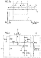
- the oscillator circuit 23 may be implemented as shown in Figure 6, in which capacitor C represents the capacitance of the conductive plates 7, 9 and the path P of the coin 1 is shown passing between the conductive plates 7,9.
- the oscillator circuit 23 is an LC tuned oscillator.
- the values of the capacitance and inductance in the circuit will determine the oscillator frequency.
- the capacitance provided by the conductive plates 7, 9 can be arranged to be of the order of 2 to 3 pF. This should provide a significant proportion of the total capacitance in the circuit, so that alterations of this capacitance due to the presence of a coin will result in a detectable change in the resonant frequency.
- the collector of the transistor in the oscillator circuit 23 has a low impedance connection to ground for a.c. signals at the resonant frequency whereas the connection between the capacitors and the inductor has a high impedance connection to ground for a.c. signals at the resonant frequency. Therefore the conductive plate connected to the collector of the transistor has a low impedance connection to ground via the 2k ohm collector resistor and the conductive plate connected to the inductor has a high impedance connection to ground.
- the conductive plate with the high impedance connection is more sensitive to unwanted external signals, and therefore circuit operation is improved if it is given additional shielding.
- this is conveniently provided by arranging the circuit board carrying the detection circuit 11 so that the conductive plate with the high impedance connection is sandwiched between the conductive plate with the low impedance connection and the circuit board. In this way shielding is provided by the conductive plate with the low impedance connection and by the ground plane of the circuit board.
- the buffer 25 may be provided by an emitter follower stage, which prevents the input of the frequency divider 27 loading the oscillator circuit 23 excessively.
- the 6 MHz output of the frequency divider 27 is fed via the co-axial cable 19 to a pulse shaper 29 of the signal processing portion 12.
- the pulse shaper 29 squares the waveform of the signal received over the co-axial cable 19 and provides it to the clock input of a counter 31.
- the counter 31 is controlled by a microprocessor 35 to count the oscillations of the signal received at its clock input from the detection circuit 11.
- the counter 31 is stopped by the microprocessor 35 and the contents of the counter 31 are loaded in parallel into a shift register 33 under control of the microprocessor 35.
- the counter 31 is reset and starts counting for the next counting period.
- the contents of the shift register 33 are then serially loaded into the microprocessor 35.
- the microprocessor 35 receives, via shift register 33, the count value of the counter 31.
- This count value equals the number of output cycles of the frequency divider 27 of the detection circuit 11 during the counting period. Consequently, this count value gives a measure of the frequency of the signal produced by the oscillator circuit 23.
- a look-up table is provided in a memory 37.
- the look-up table stores coin denomination information with reference to count value.
- an optical diameter detection system comprises an LED 20 and an optical sensor 21 positioned opposite each other on the guide 3 of Figure 1.
- the LED 20 and optical sensor 21 are spaced at a predetermined height above the floor 4 of the guide 3.
- a coin of greater diameter than the predetermined height will intercept the light beam from the LED 20 to the optical sensor 21, and accordingly it can be distinguished from a coin of lesser diameter than the predetermined height.
- the predetermined height is chosen so as to distinguish between pairs of coins which have similar effects on the oscillation frequency of the oscillator circuit 23.
- the LED 20 is powered by an optical sensor control circuit 22, which also receives the output signal from the optical sensor 21.
- the optical sensor control circuit 22 outputs an optical sensing signal to the microprocessor 35.
- the memory 37 comprises three registers, Store A 41, Store B 43 and Difference register 45 and the look-up table 47.
- Store A 41 contains a reference frequency value of 60000 (the number of oscillation of a 6MHz signal in 10ms counting period).
- the count value from the shift register 33 is loaded into Store B 43.
- the microprocessor 35 then calculates the difference between the count value in Store B 43 and the reference frequency value in Store A 41. The difference is stored in the Difference register 45.
- the maximum frequency of the signal will be the 192 MHz frequency output when no coin is present between the conductive plates 7, 9.
- the number of pulses supplied to the counter 31 in a 10 ms counting period will not exceed 60000, which is well within the counting range of a 16-bit binary counter.
- the counter 31 and the shift register 33 are both 16-bit binary devices, and Store A 41 and Store B 43 are 16-bit registers.
- a relatively large coin such as the British £1 and 50p coins, may alter the capacitance of the conductive plates 7, 9 by about 0.7pF, and the corresponding change in the frequency of the oscillator circuit 23 will result in a difference between the value stored in Store A 41 and the value stored in Store B 43 which can be represented as a 12-bit binary number.
- Slight instabilities in the oscillator circuit 23 may cause slight variations in the precise 12-bit value, but these can be accommodated by discarding the bottom 4 bits, and storing only the top 8 bits in the Difference register 45. Consequently, the Difference register 45 can be implemented by an 8-bit register.
- Figures 5a and 5b illustrate the difference values stored in the Difference register 45 for successive 10ms counting periods as a coin 1 passes between the conductive plates 7, 9.
- the difference value stored in the Difference register 45 by the microprocessor 35 in each counting period will increase rapidly to a maximum as shown in Figure 5b.
- the maximum value is maintained while the coin 1 is fully between the conductive plates 7, 9 (e.g. at position la) and then decreases sharply as the coin 1 leaves the conductive plates 7, 9 (at position 1c).
- the difference value returns substantially to zero.
- the microprocessor 35 determines the maximum frequency difference and uses it to interrogate the look-up table 47.
- the look-up table 47 contains an entry for each possible difference value determined by the microprocessor 35 and corresponding coin validation information. For each possible difference value, the microprocessor 35 receives information enabling it to determine whether the coin is valid or invalid, and also to determine the denomination of a valid coin.
- the optical sensing signal from the optical sensor control circuit 22 is also input to the look-up table 47.
- Table 1 gives an example of the contents of the look-up table 47. Different systems will have different values for each valid coin, and the values given are just an example.
- a difference value of 90 can be either the highest acceptable difference value for a new (1992) ten pence piece or the lowest acceptable difference value for a two pence piece.
- a difference value of 195 indicates either a one pound coin or a fifty pence coin.
- the height of the LED 20 and the optical sensor 21 above the floor 4 of the guide 3 is chosen so as to enable both of these ambiguities to be resolved by the optical sensing signal.
- the output of the optical sensor control circuit 22 will indicate '1' for a two pence coin and a fifty pence coin and '0' for a one pound coin and new ten pence coin.
- the microprocessor 35 If the difference value from the look-up table 47 corresponds to a valid coin, the microprocessor 35 indicates to a control circuit 39 that the coin 1 is a valid coin of the denomination indicated by the look-up table 47. In response to this coin validation information the control circuit 39 will control the operation of, for example, the coin operated telephone or vending machine. If the difference value received by the microprocessor 35 corresponds in the look-up table 47 to an invalid coin, the microprocessor 35 will inform the control circuit 39 of this, and the control circuit 39 may e.g. reject the coin 1.
- control circuit 39 is shown separately from the microprocessor 35. In practice it may be a separate piece of hardware or alternatively its function may be implemented by a program run in the coin validation microprocessor 35.
- the circuit of Figure 3 is advantageous because it can be constructed to operate with a power consumption of about 10mA with a 4.5V or 5V supply, especially if the control function of the control circuit 39 is provided by software within the microprocessor 35.
- This power consumption is sufficiently low that the circuit can act as a coin validator in a payphone powered only by the power available from the telephone line connection. In this way, the need for electric power cells or a mains electricity connection can be avoided.
- the most significant power consumption in the circuit is typically in the frequency divider 27. If this is provided by an emitter coupled logic high speed chip such as chip type SP 8797 of Plessey Semiconductors, it will draw about 7mA.
- the microprocessor 35 varies the reference frequency value stored in Store A 41 in response to variations in the count value obtained in the absence of a coin. Such variations may occur, for example, owing to changes in the oscillation frequency of the oscillator circuit 23 with temperature.
- a count value is supplied to the microprocessor 35 from 16-bit counter 31 in each counting period and is stored in Store B 43 of memory 37. Then the difference is calculated between the values stored in Store A 41 and Store B 43. If the value in Store A 41 is greater than the value in Store B 43, Store A 41 is incremented by 1 and if the difference is the other way round, Store A 41 is decremented by 1.
- a value which follows the frequency of the oscillator signal is maintained in Store A 41 of memory 37, and the system is automatically compensated for frequency drift in the oscillator circuit 23.
- drift compensation may be important. For example, in the circuit described above a frequency drift of 0.1% in the oscillator circuit will change the count value in Store B 43 by 60. If the value in Store A 41 is not altered correspondingly, the difference values will also change by 60 and a look-up table in accordance with Table 1 would cease to provide the correct output.
- the microprocessor 35 can be programmed to identify the presence of a coin 1 from -a large difference value, e.g. a value in excess of 20 in the case of the Table 1 difference values, and may suspend its function for updating the contents of Store A 41 under these circumstances. This prevents the updating function from artificially reducing the difference values generated by the coin. However, if the microprocessor 35 is programmed to use the largest difference value obtained from a coin, and the contents of the look-up table 47 are prepared appropriately, it may not be necessary to turn off the updating function. In this case, any difference value which has been significantly reduced by the effect of the updating function will not be the largest value, and accordingly it will not be used for coin validation.
- a large difference value e.g. a value in excess of 20 in the case of the Table 1 difference values
- a compensation value may be stored in the memory 37.
- the microprocessor may increment or decrement this compensation value instead of the value in Store A 41.
- the difference value between the values in Store A 41 and Store B 43 when no coin is present may be stored as the compensation value.
- the compensation value is used to compensate the difference value in the Difference Register 45 or the values read from the look-up table 47 when a coin is present.
- the microprocessor 35 may be set into a training mode. When the microprocessor 35 is in the training mode a number of valid coins may be passed through the coin validator and the microprocessor 35 will store in the look-up table 47 a range of frequency differences and optical sensor pair input values which represent each of the valid coins.
- the training exercise above will normally be carried out for each coin validation system separately although in some cases it may be possible for training to be carried out centrally and an updated look-up table reproduced and provided to other suitable coin validation systems by exchanging memory chips.
- Suitable values for the inductance and the capacitance in the circuit of Figure 6 can provide a resonant frequency of around 200 MHz (e.g. 192 MHz as previously stated).
- the resonant frequency of the oscillator circuit 23 can be increased above 200 MHz by replacing the 3.3pF capacitor in parallel with the conductive plates 7, 9 by a lower value capacitor, or removing it altogether. This will tend to increase the effect of a coin 1 on the resonant frequency. Reducing the value of the inductor will also increase the resonant frequency of the circuit, but the value of the inductor should be maintained large in comparison with the inherent inductance of the circuit wiring and other components to ensure that the circuit operates in a predictable manner. In practice it may be difficult to provide a circuit having a resonant frequency above about 0.5 GHz.
- the oscillator circuit 23 can also be arranged to have a resonant frequency lower than 192 MHz. If a much lower frequency is desired, the circuit designer should take account of the consequences of this on the operation of the analysis circuit. If the total circuit capacitance is increased to lower the frequency, the effect of the coin 1 on the frequency will tend to reduce, making it harder to detect the presence of a coin 1 and to distinguish between different coins. If the total circuit capacitance is maintained unchanged, and the resonant frequency is lowered solely by increasing the inductance in the circuit, the effects of the inherent resistance and inherent capacitance of the inductor become more significant, causing unsuitable circuit operation.
- the analysis circuit of Figure 3 throws away the bottom 4 bits of the difference between the counter value stored in Store B 43 and the reference value stored in Store A 41. These bits are treated as noise due to frequency instability in the oscillator circuit 23. Consequently, the smallest detectable frequency change is one which leads to a change of at least 16 in the value counted by the counter 31, which is a change of about 0.027%. Under these circumstances, it is difficult in practice to provide a usable oscillator circuit with a resonant frequency below 10 MHz, and a resonant frequency above 20 MHz will normally be necessary. Preferably the resonant frequency is at least 50 MHz, more preferably at least 100 MHz.
- the oscillator circuit 23 is sufficiently stable, some or all of the lowest 4 bits of the calculated difference can be relied on as a measure of coin characteristics, instead of being ignored as noise. In this case, a smaller percentage change in oscillator frequency is measurable, provided that the lowest 4 bits of the calculated difference between the values in Store A 41 and Store B 43 are not thrown away before the difference value is stored in the Difference register 45.
- the ability to measure a smaller percentage frequency change allows the capacitance in the oscillator circuit to be increased. This in turn allows the operating frequency of the oscillator circuit 23 to be reduced. If the circuit of Figure 3 is modified in this way, it may be possible to increase the capacitance in parallel with the conductive plates 7,9 to 10 to 15 pF, and to select the inductance to bring the nominal operating frequency of the circuit to 12 MHz.
- the circuit of Figure 3 is further modified by removing the frequency divider 27.
- the pulse shaper 29 now receives a signal at 12 MHz instead of 6 MHz.
- the counter 31 is operated as before, but in 10ms it will overflow once so that its output will be in effect the bottom 16 bits of a 17 bit count.
- the value in Store A 41 representing the count value for 12 MHz, will nominally be 54464 (the excess of 120000 counts over the overflow value of the counter 31, which is 65536), but it can be updated to track frequency drift as discussed above.
- the Difference register 45 may store the full 12 bits of the calculated difference, or it may store an 8-bit difference value by choosing the appropriate 8 bits to provide reliable coin identification (e.g.
- the lowest practical oscillator frequency for the oscillator circuit 23 can be reduced below 10 MHz, to 5MHz or even to 1 MHz.
- a resonating circuit is formed by capacitor C1 and inductor L1.
- the conductive plates 7, 9 are connected across terminals JP1, to provide an additional capacitance in parallel with the capacitor C1.
- Terminals JP2 are normally shorted together. In this way, an LC oscillator is provided having a natural oscillation frequency which is altered by the presence of a coin between the conductive plates 7, 9 of the coin guide 3.
- the oscillator is driven by transistors Q2 and Q3. These two transistors have identical dc bias arrangements for their bases, which are connected through respective resistors R7 and R8 to a common node which is in turn connected through matching resistors R5 and R6 to both the positive line voltage V2 and the negative line voltage Vss.
- the oscillating voltage from the junction between capacitor C1 and inductor L1 is applied to the base of transistor Q3 through dc isolating capacitor C4, and is also applied directly to the collector of Q2.
- transistor Q3 is turned on through C4 and current flows through emitter resistor R13, which is common to both transistor Q3 and transistor Q2.
- transistor Q2 This raises the emitter potential, tending to turn transistor Q2 off, so that its collector connected to the junction between capacitor C1 and inductor L1 can remain high.
- transistor Q3 When the junction between the capacitor C1 and inductor L1 goes low, transistor Q3 is turned off through capacitor C4, so that it does not provide any current to emitter resistor R13, so that the emitter voltage can fall to the line voltage Vss, and transistor Q2 will tend to turn on owing to its dc bias through resistor R7. Thus, it will tend to conduct current from its collector, pulling down the junction between capacitor C1 and inductor L1. In this manner, the circuit of transistors Q2 and Q3 drives the oscillator.
- the output signal is taken from the collector of transistor Q3, which in this respect acts as a common emitter coupled amplifying transistor.
- Inductance L2 is provided so that the collector load for transistor Q3 is partly inductive.
- the buffer 25 is provided by pnp transistor Q4, which also acts as a common emitter connected amplifier, and provides its output from its collector through dc isolating capacitor C11.
- Coil L3 provides an inductive collector load for transistor Q4, to magnify the voltage swing at the collector of transistor Q4.
- the oscillator circuit of Figure 7 is preferred at present, because it appears to provide better stability of the oscillator frequency with changes of temperature and changes of component values over time as compared with the circuit of Figure 6.
- the frequency divider 27 of Figure 3 is not used.
- the output from the buffer transistor Q4 is provided through the capacitor C11 to an input of an application specific integrated circuit (ASIC).
- a diode D1 acts as a dc clamp/level shifter, to ensure that the input to the ASIC does not go lower than about 0.4 volts below line voltage Vss, to ensure that the oscillating voltage provided to the ASIC is within a suitable voltage range.
- the pulse shaper 29 of Figure 3 is not required, because the inductance L3 ensures that the voltage swing at the input to the ASIC is sufficient to clock the counter 31.
- the ASIC contains the counter 31 and shift register 33 of Figure 3. It provides an output for the microprocessor 35 and has input connections to receive signals from the microprocessor.
- the circuit of Figure 7 is designed for use in a pay telephone, in which the microprocessor 35 is provided on the main circuit board of the telephone, and the ASIC is connected to the microprocessor through a plug connector PL1 for connecting the coin validator circuit board to the main circuit board of the telephone.
- the circuit can be constructed to operate with a power consumption of about 5mA at 4.5V or 5V.
- the counter 31 in the ASIC receives the output of buffer 25, and the remainder of the analysis circuit operates as described above with reference to Figure 3, except that at least some of the lowest 4 bits of the calculated difference are used to determine the characteristics of the input coin.
- the Difference Register 45 is a 12-bit register storing all bits of the difference value.
- the look-up table 47 contains 12-bit values, between 0 and 4095 (or 000 and FFF in hexadecimal notation). Table 2 gives an example of the contents of the look-up table 47 using 12-bit values.
- the new 10p coin and the 2p coin can be discriminated on the basis of the difference value without confusion, and the optical sensing arrangement is used only to discriminate between the £1 coin and the 50p coin.
- the Difference Register 45 may be convenient to provide as a 16-bit register, similar to the Store A and Store B registers, even though the difference value is unlikely to require more than 10 or 11 bits.
- the plug connector PL1 also carries connections by which the microprocessor 35 is able to drive one or two optical detector devices S1, S2. These are units which comprise a light emitting diode associated with a photosensitive transistor, arranged so that if a coin is present the light emitted by the diode will be reflected back to the unit and detected by the photosensitive transistor.
- Line 1 of the plug connector PL1 is a drive line for the light emitting diodes. When this line goes high, transistor Q1 turns on and current passes through the light emitting diodes, causing them to emit light.
- Each optical sensor unit provides an equivalent to the LED 20 and the optical sensor 21.
- unit S1 may be omitted and the position of its light emitting diode is shorted by providing a link between terminals JP3.
- the optical sensor unit S2 is used to detect when a coin enters the coin guide 3, before it reaches the conductive plates 7, 9, so as to prepare the microprocessor 35 for conducting a coin validation operation.
- the optional optical sensor S1 can be used to provide a coin height discriminator, to distinguish between large diameter coins and small diameter coins having the same effect as each other on the capacitance between the conductive plates 7, 9, as described above with reference to the LED 20 and the optical sensor 21. Alternatively it can be used as part of an arrangement to detect attempts fraudulently to remove a coin from the coin guide 3 after insertion. Additionally, fraudulent withdrawal of a coin after it has been inserted into the coin guide can alternatively be prevented by mechanical means, such as a flap which is pressed down by the coin as it enters the guide and which rises behind the coin to prevent fraudulent withdrawal.
- the circuit of Figure 7 can be constructed on a single circuit board, with the microprocessor 35 on the main control circuit board of the payphone or other apparatus controlled by the coin validator. Conveniently, all of this circuitry can be provided inside the protective box 13, so that connections may be provided by simple wires and the co-axial cable 19 is not required.
- a coin If a coin is strongly electrically conductive, its effect on the capacitance between the conductive plates 7,9 will largely be. a function of its area (i.e. a function of its diameter) and its thickness. While the coin is between the conductive plates 7, 9, its electrically conductive substance will replace part of the air in the gap between the conductive plates 7, 9, and accordingly it will reduce the effective thickness of the dielectric for part of the capacitor formed by the conductive plates 7, 9.
- the part of the capacitor which is affected in this matter will be the part where the coin is present, that is to say, the part defined by projecting the outline of the coin onto the conductive plates 7,9. Therefore the larger the area of the coin is, the greater is the part of the capacitor which is affected.
- the degree to which the capacitance of the affected part of the capacitor is altered depends on the thickness of the coin. The greater the thickness of the coin is, the more it will reduce the effective thickness of the dielectric of the affected part of the capacitor.
- a thin coin of large area will have a small effect over a large part of the capacitor and a thick coin of small area will have a large effect over a small part of the capacitor, and it is possible that the overall effect on the capacitor will be the same in each case.
- the width between the conductive plates 7, 9 is altered without changing the size of the conductive plates 7, 9, the effect of the area of a coin on the capacitance is unchanged but the effect of coin width on the capacitance is altered. Therefore, where a pair of coins, one thin and large area and the other thick and small area, have similar effects on the capacitance and are hard to distinguish, use of a different separation between the conductive plates 7, 9 will render them distinguishable.
- FIG 8 is a schematic view from above of the coin guide 3 together with the conductive plates 7,9
- Figure 9 is an electrical model of the construction of Figure 8.
- the total capacitance C between the conductive plates 7,9 is now treated as being the overall capacitance of three capacitors C1,C2,C3 in series.
- C1 is the capacitance of the air gap between the side walls 2 of the coin guide 3, the air gap having a width D1.
- C2 is the capacitance of the side wall 2 next to the first conductive plate 7, the side wall having a thickness D2.
- C3 is the capacitance of the side wall 2 of the coin guide 3 next to the second conductive plate 9, the side wall having a thickness D3.
- FIG 10 is a schematic top view of the coin guide 3 with a coin 1 present between the conductive plates 7,9
- Figure 11 is an electrical model of Figure 10.
- the left hand path in Figure 11 has an overall capacitance CA, and is made up of capcitances C10,C20 and C30 in series, where C10,C20 and C30 correspond to C1,C2 and C3 in Figure 9 but are the capacitances of the air gap and the side walls for the part of the area of the conductive plates 7,9 where the coin is absent.
- the right hand path in Figure 11 has an overall capacitance CB, and is made up of capacitances C11,C12,C21 and C31 in series.
- C21 and C31 are the capacitances of the parts of the side walls 2 of the coin guide 3 opposite the coin 1
- C12 is the capacitance of the coin
- Cll is the capacitance of the reduced-width portion of the air gap next to the coin 1.
- C10 Eo x (Ap-Ac)/D1
- C20 Eo x Er x (Ap-Ac)/D2
- C30 Eo x Er x (Ap-Ac)/D3
- C11 Eo x Ac/(D1-Dc)
- C12 Eo x Ec x Ac/Dc
- C21 Eo x Er x Ac/D2
- C31 Eo x Er x Ac/D3
- Ac is the area of the coin
- Dc is the thickness of the coin
- Ec is the permittivity of the coin.
- the coin guide 3 in order to distinguish between confusable coins, can be provided with two or more distinct portions which are different from each other in a relevant parameter (e.g. D1), such that a coin 1 has a different effect on the capacitance between the conductive plates 7, 9 when the coin 1 is in one portion as compared with when the coin 1 is in another portion.
- a relevant parameter e.g. D1
- Coins which would be confusable in one portion e.g. with one value of D1
- will normally be distinguishable in a different portion e.g. with a different value of D1).
- the coin guide 3 so as to vary the permittivity Ec of the coin or the thickness Dc of the coin
- it is possible to vary the effective area Ac of the coin by shaping the conductive plates 7,9 so that in one region of the coin guide only a part of the area of the coin 1 is between the plates 7,9. If the cut away part of the conductive plates 7,9 is immediately above the level of the floor 4 of the coin guide 3, both the area of the coin 1 which is not between the conductive plates 7,9, and the proportion of the total coin area represented by the area not between the plates 7,9 will be different for different diameter coins.
- widths D1,D2 and D3 and the permittivity of the side walls 2 of the coin guide 3 may be varied for only part of the height of the coin guide 3, and different regions of the coin guide 3 may be provided by successively changing the height to which the value of a parameter is changed without making further changes to the value itself.
- the conductive plates 51 are divided into a first portion 53 and a second portion 55. In the first portion 53 the conductive plates 51 do not extend down to the bottom of the guide 3, whereas in the second portion 55 the conductive plates 51 do extend down to the bottom of the guide 3.
- Figure 12a shows a large diameter (large area) thin coin 1' and a small diameter (small area) thick coin 1" passing between the conductive plates 51
- Figure 12b shows the difference values which will be stored in difference register 45 for each counting period as the coins 1', 1" pass between the conductive plates 51.
- the difference values for the large diameter coin 1' are shown by circles in Figure 12b and the difference values for the small diameter coin 1" are shown by crosses in Figure 12b.
- the difference values obtained for the coins 1', 1" when they are at positions 1'b, 1"b wholly within the second portion 55 are the same as each other, as shown in Figure 12b.
- the small diameter coin 1" is at position 1"a, wholly within the first portion 53, a substantial proportion of the coin area is below the bottom of the conductive plates 51, and its effect on the capacitance of the conductive plates 51 is much reduced. Consequently, the difference value obtained at this time is much lower.
- the large diameter coin 1' is at position l'a, wholly within the first portion 53, the part of the coin area below the bottom of the conductive plates 51 is a small proportion of the total area, and the difference value obtained is not much lower than the difference value obtained when the coin is within the second portion 55.
- optical sensor pairs 57 and 59 indicate respectively that the coin 1 is fully within the first portion 53 and the second portion 55 of the conductive plates 51.
- FIG. 13a Another embodiment of the invention as shown in Figure 13a has a first plate 61 which is planar and a second plate 63 which is stepped, to form a capacitor with a first portion 65 and a second portion 67.
- the plates 61, 63 have a smaller separation in the first portion 65 than in the second portion 67. Consequently the capacitance of the first portion 65 is greater than the capacitance of the second portion 67.
- the detection circuit 11 will produce two distinct difference values. The effect of changing the separation between the conductive plates is discussed above. Since different coins which are confusible at one separation can be distinguished at another, the two distinct difference values of Figure 13b allow such coins to be distinguished.
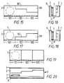
- FIG. 14a A further embodiment of the invention is shown in Figure 14a where a capacitor is formed by two plates 69, the bottom edges of which slope over the distance travelled by a coin 1 between the plates 69 along coin path P.
- This embodiment operates in substantially the same manner as the embodiment of Figure 12a, except that the difference values increase steadily with position along the plates 69 as shown in Figure 14b, instead of changing in a step fashion between two levels as shown in Figure 12b.
- optical sensor pairs 57, 59 are shown which enable the microprocessor 35 to determine when a coin 1 reaches predetermined positions between the conductive plates.
- Figure 15 is a side view of one of the side walls 2 of a coin guide 3 according to another embodiment
- Figure 16 is an end view of the coin guide 3 for the same embodiment.
- the length of the coin guide 3 can be divided into three sections 101,103,105.
- the side wall 2 has a uniform thickness.
- the side wall has the same thickness as in the first section 101 over most of its height, but an upper part 107 of the side wall has a reduced thickness.
- the width D2 of the side wall is reduced, and the width D1 of the air gap is increased.
- the effect of the coin 1 on the overall capacitance C of the conductive plates 7,9 will be different when the coin is in the second section 103 of the coin guide 3 from when it is in the first section 101.
- the effect of the reduced-thickness part 107 of the side wall 2 in the second section 103 of the coin guide 3 will tend to enable the coins to be distinguished from one another, provided that at least one the coins has sufficient diameter to overlap the reduced-thickness part 107.
- a lower part of the side wall 2 retains the original thickness and upper part 109 of the side wall 2 has the same reduced thickness as the upper part 107 of the side wall 2 in the second section 103.
- the reduced-thickness part 109 of the side wall 2 extends down lower than the reduced-thickness part 107 of the side wall 2 in the second section 103.
- the effect of a coin on the overall capacitance C between the conductive plates 7,9 will be different when the coin is in the third section 105 of the coin guide than when the coin 1 is in the first section 101 or the second section 103 of the coin guide, provided that the coin has a diameter sufficient for it to overlap the reduced-thickness part 109 of the side wall 2.
- a coin has a different effect on the overall capacitance C when it is in the third section 105 from when it is in the second section 103, although the two thicknesses for the side wall 2 are the same as in the second section 103. It is not necessary for the reduced-thickness part 109 of the side wall 2 in the third section 105 of the coin guide to have a different thickness from the reduced-thickness part 107 of the side wall 2 in the second section of the coin guide 103.
- the illustrated difference in the way in which the full thickness part of the side wall 2 and the reduced-thickness part of the side wall 2 are distributed, with the reduced-thickness part of the side wall 2 being greater in the third section 105 than in the second section 103, is sufficient to provide a difference in the way in which a coin 1 will affect the overall capacitance C between the conductive plates 7,9 when the coin 1 is in the respective section of the coin guide 3.
- Figure 17 is a side view of a side wall 2 of the coin guide 3 in a further embodiment of the present invention
- Figure 18 is an end view of the coin guide 3 of Figure 17.
- a side wall 2 of the coin guide 3 has reduced-thickness portions 107,109 in the second and third sections 103,105 of the coin guide 3, so as to change the effect that a coin 1 has on the overall capacitance C between the conductive plates 7,9, in a similar manner to the arrangement of Figures 15 and 16.
- the reduced thickness parts of the side wall 2 are provided below the full thickness portions, rather than above them as in the arrangement of Figures 15 and 16.
- the reduced-thickness sections 107,109 of the side wall 2 are present at the bottom of the side wall 2, and extend upwardly by different amounts in the second and third sections 103,105 of the coin guide 3. In this way, even a small diameter coin will have a different effect on the capacitance C between the conductive plates 7,9 in each of the three sections 101,103,105 of the coin guide 3.
- Figure 19 is a side view of a side wall 2 of another embodiment of the present invention
- Figure 20 is a top view of the coin guide 3 in the embodiment of Figure 19.
- the thickness of the side wall 2 is reduced in the second section 103 of the coin guide relative to its thickness in the first section 101 of the coin guide, over the entire height of the side wall 2.
- the thickness of the side wall 2 is reduced further, again over the entire height of the side wall 2. Accordingly, the values of the thickness D2 of the side wall and the width D1 of the air gap are different for each of the three sections 101,103,105 of the coin guide 3.
- Figure 21 is a side view of a side wall 2 in a further embodiment of the present invention
- Figure 22 is a top view of the coin guide 3 in the embodiment of Figure 21
- Figure 23 is an end view of the coin guide 3 in the embodiment of Figure 21.
- the side wall 2 of the coin guide 3 has a different thickness over its entire height in the second section 103 of the coin guide as compared with the first section 101 of the coin guide.
- this embodiment resembles the embodiment of Figures 19 and 20.
- this embodiment resembles the embodiment of Figures 15 and 16 in that the thickness of a lower part of the side wall 2 of the coin guide 3 in the third section 105 of the coin guide 3 is the same as the thickness of the side wall 2 in the second section 103 of the coin guide 3.
- the side wall 2 is absent completely rather than being present with a reduced thickness.
- the conductive plate 7 is also absent completely in the upper part of the third section 105 of the coin guide 3 in this embodiment.
- the conductive plates 7,9 are provided by printing a conductive ink on the side walls 2 of the coin guide 3, it is not practical to provide a part of the conductive plate 7 where there is no side wall 2. However, it would be possible to provide the conductive plate 7 even where there is no side wall 2 in arrangements where the conductive plate 7 is provided by a separate conductive plate bonded to the side wall 2.
- Figure 24 is a side view of a side wall 2 in a another embodiment of the present invention
- Figure 25 is an end view of the coin guide 3 in the embodiment of Figure 24.
- the physical dimensions of the side wall 2 are not altered between the sections 101,103,105 of the coin guide 3. Instead, the side wall 2 is made of a different dielectric material in each of the three sections.
- the values of the relative permittivity of plastics materials suitable for use in the coin guide 3 will typically be between 2 and 6.
- the different materials are chosen to have different relative permittivities, so that the value Er will be different in each of the three sections 101,103,105 of the coin guide 3. In this way, the effect of the coin 1 on the overall capacitance C between the conductive plates 7,9 will be different for each of the sections 101,103,105.
- Figures 12 to 25 provide some examples of the ways in which changes can be made in the effective values of D1,D2,Er and Ac, so that coins which cannot be distinguished on their effect while they are in one section of the coin guide 3 can be distinguished by their effect when they are in another section of the coin guide 3.
- a coin validator will normally be set up for use with a particular predetermined coin set. Substantially the same coin validator can be manufactured for use with a variety of coin sets, and the particular coin set for which it is to be used is determined by the difference values stored in the look up table, by which the effect of a coin on the capacitance between the conductive plates 7,9 is translated into a coin recognition or rejection.
- the width of the air gap D1 in a coin guide 3 must be sufficient to permit the thickest coin of the coin set to pass along the guide 3 without obstruction. Where a validator is made for use with a variety of possible sets of coins, the width of the thickest coin in one coin set may be different from the width of the thickest coin in another coin set. Therefore, the coin guide may have a width D1 of the air gap which is larger than is necessary for use with some of the coin sets.
- the width D1 of the air gap is reduced, the effect of the presence of a coin 1 on the capacitance between the conductive plates 7,9 will tend to be increased, making it easier for the validator to detect the presence of a coin.
- the increased values in the change of the capacitance C also tends to make it easier to distinguish between the different coins of the coin set.
- the effect of reducing the width of the air gap D1 remains even if the thickness D2 of the side walls are increased by a corresponding amount, because the relative permittivity Er of the material of the side walls 2 is greater than 1 so that the overall capacitance C is increased by filling part of the air gap with the material of the side wall 2.
- Figure 26 is a side view of an insert 111 of dielectric material, which may be attached to the inner side of a side wall 2 of the coin guide 3, as shown in Figure 27. In this way, part of the width of the air gap D1 is filled with dielectric material.
- the width of the air gap D1 can then be adapted at low cost by attaching an appropriate insert 111 to take into account the thickness of the thickest coin in the coin set with which the validator is to be used.
- an insert 111 can be used as a means of providing the difference between the first section 101, second section 103 and third section 105 of the coin guide 3 as discussed with reference to Figures 15 to 25.
- Figure 28 shows a side view of an insert 111 having a stepped height, so that when it is attached to one of the side walls 2 an arrangement is obtained which is equivalent to the embodiment of Figures 15 and 16.
- Figure 29 shows a top view of an insert 111 having a stepped thickness, so that when such an insert is attached to a side wall 2 an arrangement is provided corresponding to the embodiment of Figures 19 and 20.
- Figure 30 shows an insert 111 in which different sections are made of materials having different relative permittivities, so that when such an insert is attached to a side wall 2, an arrangement is provided corresponding to the embodiment of Figures 24 and 25. This allows the manufacturing convenience of making standard uniform coin guides 3, and separately manufacturing a range of inserts to define the different sections 101,103,105 of the coin guide 3.
- the coin guide 3 will normally be set at a sideways tilt so that the coin always rests against one of the side walls 2 and does not contact the other, as shown in Figure 2.
- the different sections of the coin guide are defined by differences in the physical dimensions of a side wall 2, and particularly in cases where the thickness of a side wall 2 changes, it is normally preferable for the side wall having the physical variations to be the side wall against which the coin 1 does not rest, so that the variations in the physical dimension of the side wall 2 do not interefere with the smooth rolling of the coin 1 along the coin guide 3.
- Figure 31 shows an alternative circuit to that in Figure 3 where the output of the oscillator 77 is fed into a frequency divider 79 via a buffer 81, similarly to the circuit of Figure 3, but the output of the frequency divider 79 is fed via a co-axial cable 83 to a mixer 85 instead of to the pulse shaper 29 of Figure 3.
- the mixer 85 the signal is mixed with a reference signal of known frequency produced by a reference oscillator 87.
- the resulting signal has a lowest frequency component which represents the difference between the reference frequency and the detection signal frequency from the frequency divider 79.
- This mixed frequency signal is passed to a low-pass filter 89 to obtain the frequency difference signal which is passed to a pulse shaper 91, then to a frequency divider 93 and then to a microprocessor 95 where the frequency difference is compared to the range of frequency differences for known valid coins which are stored in memory 97. If the frequency difference matches that of a known valid coin, the microprocessor 95 indicates to the control circuit 99 that the coin is valid and of a particular denomination and if the frequency difference is not matched against that of known valid coin, the microprocessor 95 sends a signal to the control circuit 99 to indicate that the coin 1 is invalid and should be rejected.
- the microprocessor 95 determines the difference frequency by counting pulses received from the frequency divider 93 in a preset period.
- the frequency divider 93 is used to scale the difference frequency so that the number of pulses counted by the microprocessor does not overflow its internal registers.
- This circuit may be compensated for drift in the rest frequency of the oscillator 77 by making a corresponding change to the frequency of the reference oscillator 87. This is the equivalent in this arrangement to varying the reference value in Store A 41 in the arrangement of Figures 3 and 4.
- the frequency divider 79 is not necessary if the oscillator circuit 77 operates at a sufficiently low frequency, such as the 6MHz proposed for the circuit of Figure 7. Additionally, the co-axial cable 83 is not needed if the components are housed in a common protective box 13.
- the illustrated embodiments provide a coin validator of simple construction, and in which the structure of the validator does not wholly determine which coins can be detected and accepted. Modification of the validator to alter which coins are acceptable can be carried out easily since it will often only be necessary to change the contents of the look-up table.
Landscapes
- Physics & Mathematics (AREA)
- General Physics & Mathematics (AREA)
- Testing Of Coins (AREA)
- Prostheses (AREA)
- Heat Treatment Of Steel (AREA)
- Noodles (AREA)
- Acyclic And Carbocyclic Compounds In Medicinal Compositions (AREA)
- Control Of Metal Rolling (AREA)
Claims (27)
- Appareil pour déterminer si une pièce de monnaie introduite est acceptable et pour faire la distinction entre une pluralité de pièces acceptables, comprenant:des moyens formant condensateur (7, 9)des moyens de guidage (3) pour guider une pièce de monnaie introduite (1) le long d'un trajet de circulation de pièces dans les moyens formant condensateur, de manière à affecter sa capacité quand la pièce de monnaie est dans une première position du trajet de circulation des pièces,des moyens formant oscillateur (23) pour émettre un signal de sortie oscillant dont la fréquence est affectée par la capacité des moyens formant condensateur, etdes moyens de décision (31, 33, 35, 37) pour recevoir le signal de sortie oscillant et prendre une décision, sur la base de la fréquence du signal de sortie oscillant quand une pièce de monnaie introduite se trouve dans la première partie du trajet de circulation des pièces, si la pièce introduite est acceptable, et dans ce cas, de décider de quelle pièce il s'agit parmi une pluralité de pièces acceptables, les moyens de décision étant agencés pour interpréter différentes fréquences du signal de sortie oscillant comme représentant la présence de pièces de monnaie différentes.caractérisé en ce que les moyens de décision utilisent la fréquence du signal de sortie oscillant pendant que la pièce de monnaie introduite se trouve dans une deuxième partie du trajet de circulation des pièces, pour faire la distinction entre des pièces introduites différentes qui émettent la même fréquence lorsqu'elles se trouvent dans la première partie du trajet de circulation de pièces, et en ce que les moyens formant condensateur (7. 9) et les moyens de guidage (3) sont agencés de manière qu'une pièce introduite (1) affecte la capacité des moyens formant condensateur (7, 9) pendant que la pièce est dans la deuxième partie du trajet de circulation de pièces, mais que un ou plusieurs des paramètres physiques des moyens formant condensateur, qui déterminent l'importance de l'effet d'une pièce de monnaie sur la capacité des moyens formant condensateur sont différents de la première, dans la deuxième partie de trajet de circulation de pièces.
- Appareil selon la revendication 1, dans lequel un ou plusieurs desdits paramètres physiques varient progressivement, de la première partie vers la deuxième partie du trajet de circulation des pièces.
- Appareil selon la revendication 1, dans lequel un ou plusieurs desdits paramètres physiques varient sensiblement selon une fonction pas à pas à partir de la première partie jusqu'à la deuxième partie du trajet de circulation des pièces.
- Appareil selon l'une quelconque des revendications 1 à 3. dans lequel un ou plusieurs desdits paramètres physiques comprennent la hauteur d'un bord d'une plaque de condensateur (7,9; 51; 69) des moyens formant condensateur au dessus d'un fond (4) des moyens de guidage (3) qui affecte l'importance du recouvrement entre la surface de la pièce de monnaie introduite (1) et la plaque de condensateur (7, 9).
- Appareil selon l'une quelconque des revendications 1 à 4, dans lequel un ou plusieurs desdits paramètres physiques comprennent l'écartement entre les plaques de condensateur (61, 63) des moyens formant condensateur.
- Appareil selon l'une quelconque des revendications 1 à 5, dans lequel un ou plusieurs desdits paramètres physiques comprennent l'épaisseur effective (D2) d'une pièce en matériau diélectrique entre les plaques de condensateur des moyens formant condensateur.
- Appareil selon l'une quelconque des revendications 1 à 6, dans lequel un ou plusieurs desdits paramètres physiques comprennent la constante diélectrique effective (permittivité) d'une pièce en matériau diélectrique entre les plaques de condensateur dcs moyens formant condensateur.
- Appareil selon l'une quelconque des revendications 1 à 7, dans lequel un ou plusieurs desdits paramètres physiques comprennent la largeur effective (D1) d'un intervalle d'air que traverse la pièce de monnaie introduite entre les plaques de condensateur des moyens formant condensateur.
- Appareil selon l'une quelconque des revendications 5 à 8, dans lequel la valeur de l'un desdits paramètres physiques varie en fonction de la hauteur au dessus d'un fond de la goulotte de guidage des pièces de monnaie dans l'une desdites parties du trajet de circulations des pièces.
- Appareil selon la revendication 9. dans lequel la valeur de l'un desdits paramètres physiques est la même pour lesdites deux parties de la goulotte de guidage des pièces de monnaie sur une première gamme de hauteurs au dessus du fond de la goulotte de guidage des pièces de monnaie, mais est différente pour les première et deuxième parties sur une seconde gamme de hauteurs au dessus du fond de la goulotte de guidage des pièces de monnaie, de manière que les valeurs effectives du paramètre physique concerné soient différentes dans les première et deuxième parties.
- Appareil selon l'une quelconque des revendications 1 à 10, dans lequel un élément (111) fixé sur une paroi (2) des moyens de guidage (3) crée une différence dans un ou plusieurs desdits paramètres physiques entre la première partie et la deuxième partie du trajet de circulation des pièces de monnaie.
- Appareil selon la revendication 11, dans lequel l'élément (111) n'est pas uniforme dans au moins l'une de ses données: de hauteur; d'épaisseur: et de SA composition, dans la direction le long du trajet de circulation des pièces de monnaie.
- Appareil selon l'une quelconque des précédentes revendications, dans lequel lesdits moyens de décision comprennent des moyens de comptage (31) pour compter les oscillations de la fréquence de sortie oscillante, de manière à obtenir une mesure de ladite fréquence utilisable pour prendre ladite décision.
- Appareil selon la revendication 12, dans lequel les moyens de décision comprennent des moyens (35) pour comparer la valeur de comptage atteinte par les moyens de comptage au cours d'une période de durée prédéterminée avec une valeur mise en mémoire préalablement et prendre ladite décision sur la base du résultat de la comparaison.
- Appareil selon l'une quelconque des revendications 1 à 14, dans lequel les moyens formant oscillateur comprennent un circuit oscillant suivi par un diviseur de fréquence (27).
- Appareil selon l'une quelconque des revendications 1 à 14, dans lequel les moyens formant oscillateur comprennent : un circuit oscillant (77) dont la fréquence d'oscillation est affectée par la capacité des moyens formant condensateur (7, 9); un oscillateur de référence (87); un mélangeur (85) pour mélanger le signal de sortie du circuit oscillant à la sortie de l'oscillateur de référence; et des moyens de filtrage (89) pour filtrer le signal de sortie du mélangeur de manière que la fréquence de signal de sortie oscillant en aval des moyens de filtrage soit fonction de la différence entre la fréquence de signal de sortie du circuit oscillant et la fréquence du signal de sortie de l'oscillateur de référence.
- Appareil selon l'une quelconque des précédentes revendications comprenant des moyens de compensation pour surveiller la fréquence de repos du signal de sortie oscillant en l'absence d'une pièce de monnaie et compenser les moyens de décision en cas de modification de la fréquence de repos en fonction du temps.
- Appareil selon la revendication 17, dans lequel les moyens de décision dérivent une valeur de différence représentant la différence entre la fréquence du signal de sortie oscillant en présence d'une pièce de monnaie introduite et une fréquence de référence, et prend ladite décision sur la base de la valeur de différence et d'une corrélation mise en mémoire préalablement de valeurs de différences possibles et de données d'identification de la pièce introduite.
- Appareil selon la revendication 18, dans lequel la fréquence de référence est sensiblement égale à la fréquence de repos du signal de sortie oscillant quand aucune pièce de monnaie n'est introduite.
- Appareil selon la revendication 18 ou 19, dans lequel les moyens de compensation mettent à jour la fréquence de référence pour tenir compte des variations dans le temps de la fréquence de repos du signal de sortie oscillant.
- Appareil selon l'une quelconque des revendications 18 à 20, dans lequel les moyens de décision dérivent la valeur de différence en comparant une valeur représentant la fréquence du signal de sortie oscillant à une valeur mise en mémoire au préalable. représentant la fréquence de référence.
- Appareil selon la revendication 21 dépendant de la revendication 20, dans lequel les moyens de compensation mettent à jour la fréquence de référence en mettant à jour la valeur mise en mémoire préalablement.
- Appareil selon la revendication 22, dans lequel les moyens de compensation mettent à jour la fréquence de référence en comparant la valeur mise en mémoire préalablement à une valeur représentant la fréquence de repos du signal de sortie oscillant et mettent à jour la valeur mise en mémoire préalablement en réponse au résultat de la comparaison.
- Appareil selon l'une quelconque des précédentes revendications, dans lequel le trajet de circulation des pièces passe entre les plaques conductrices (7, 9) des moyens formant condensateur.
- Appareil selon l'une quelconque des précédentes revendications, dans lequel les moyens formant oscillateur comprennent un oscillateur accordé self/capacité.
- Un procédé pour déterminer si une pièce de monnaie introduite est acceptable et pour faire la distinction entre une pluralité de pièces acceptables, dans lequel une pièce de monnaie introduite est guidée pour passer dans des moyens formant condensateur de manière à affecter leur capacité quand la pièce est dans une première position le long du trajet de circulation des pièces, des moyens formant oscillateur émettant un signal de sortie oscillant dont la fréquence est affectée par la capacité des moyens formant condensateur, et soit la pièce introduite est rejetée soit il est décidé de quelle pièce il s'agit parmi une pluralité de pièces acceptables, en se basant sur la fréquence du signal de sortie oscillant pendant que la pièce introduite est dans une première position le long du trajet de circulation des pièces, les fréquences différentes du signal de sortie oscillant étant interprétées comme représentant la présence de pièces différentes,
caractérisé en ce que la pièce de monnaie introduite est rejetée ou qu'il est décidé de quelle pièce il s'agit, parmi la pluralité de pièces acceptables, sur la base, à la fois, de la fréquence du signal de sortie oscillant quand la pièce introduite est dans la première position le long du trajet des pièces, et de la fréquence du signal de sortie oscillant lorsque la pièce est dans une deuxième position le long du trajet de circulation des pièces, et en ce que la pièce affecte également la capacité des moyens formant condensateur lorsque la pièce est dans la deuxième position le long du trajet de circulation des pièces. mais que un ou plusieurs paramètres physiques des moyens formant condensateur qui déterminent l'importance avec laquelle la pièce de monnaie affecte la capacité des moyens formant condensateur. sont différents dans la deuxième position comparativement à la première position. - Un procédé selon la revendication 26, dans lequel la fréquence de repos du signal de sortie oscillant en l'absence d'une pièce de monnaie est surveillée de manière à compenser l'étape de rejet ou de décision en cas de modifications de la fréquence de repos au fil du temps.
Applications Claiming Priority (5)
| Application Number | Priority Date | Filing Date | Title |
|---|---|---|---|
| GB9221591 | 1992-10-14 | ||
| GB9221591A GB2271875A (en) | 1992-10-14 | 1992-10-14 | Coin validator |
| GB939314508A GB9314508D0 (en) | 1993-07-13 | 1993-07-13 | Coin validators |
| GB9314508 | 1993-07-13 | ||
| PCT/GB1993/002119 WO1994009452A1 (fr) | 1992-10-14 | 1993-10-13 | Appareil de validation de pieces de monnaie |
Publications (2)
| Publication Number | Publication Date |
|---|---|
| EP0664914A1 EP0664914A1 (fr) | 1995-08-02 |
| EP0664914B1 true EP0664914B1 (fr) | 1997-06-25 |
Family
ID=26301796
Family Applications (1)
| Application Number | Title | Priority Date | Filing Date |
|---|---|---|---|
| EP93922993A Expired - Lifetime EP0664914B1 (fr) | 1992-10-14 | 1993-10-13 | Appareil de validation de pieces de monnaie |
Country Status (9)
| Country | Link |
|---|---|
| US (1) | US5687829A (fr) |
| EP (1) | EP0664914B1 (fr) |
| JP (1) | JPH08502608A (fr) |
| AT (1) | ATE154852T1 (fr) |
| DE (1) | DE69311812T2 (fr) |
| ES (1) | ES2104180T3 (fr) |
| GB (1) | GB2271659B (fr) |
| MX (1) | MX9306404A (fr) |
| WO (1) | WO1994009452A1 (fr) |
Families Citing this family (18)
| Publication number | Priority date | Publication date | Assignee | Title |
|---|---|---|---|---|
| US5485908A (en) * | 1994-07-12 | 1996-01-23 | Coin Acceptors, Inc. | Pattern recognition using artificial neural network for coin validation |
| GB2292473A (en) * | 1994-08-12 | 1996-02-21 | Tetrel Ltd | Coin validators |
| US6026946A (en) * | 1997-03-10 | 2000-02-22 | Pom, Inc. | Enhanced coin discrimination systems and methods |
| GB2331614A (en) * | 1997-11-19 | 1999-05-26 | Tetrel Ltd | Inductive coin validation system |
| GB9823970D0 (en) * | 1998-11-02 | 1998-12-30 | Coin Controls | Improved sensor for coin acceptor |
| US6267662B1 (en) * | 1999-04-13 | 2001-07-31 | Mars Incorporated | Measuring a stack of coins in a coin handling device |
| AU2000222731A1 (en) * | 2000-01-28 | 2001-08-07 | Cashcode Company Inc. | Capacitance sensor for coin evaluation |
| US6907977B1 (en) | 2000-01-28 | 2005-06-21 | Cashcode Company Inc. | Capacitance sensor for coin evaluation |
| SE521207C2 (sv) * | 2001-03-22 | 2003-10-14 | Scan Coin Ind Ab | Anordning och metod för särskiljning av mynt där en variation i kapacitans sker mellan en sensorelektrod och en yta hos myntet då myntet är under transport |
| SE522752C2 (sv) * | 2001-11-05 | 2004-03-02 | Scan Coin Ind Ab | Metod att driva en myntdiskriminator och en myntdiskriminator där påverkan på spolorgan mäts när mynt utsätts för magnetfält alstrade av spolorgan utanför myntet |
| US6920972B2 (en) * | 2002-02-01 | 2005-07-26 | Pom, Incorporated | Coin fraud detection sensing system and method |
| US7073683B1 (en) * | 2003-01-03 | 2006-07-11 | Lawrence Quinnell | Apparatus and method for determining completion of a requested transaction in a vending machine |
| ES2343730T3 (es) * | 2003-09-24 | 2010-08-09 | Scan Coin Ab | Discriminador de monedas. |
| US20080033596A1 (en) * | 2006-07-06 | 2008-02-07 | Fausak Andrew T | Vision Feedback Detection for Vending Machines and the Like |
| JP5130773B2 (ja) * | 2006-07-18 | 2013-01-30 | パナソニック株式会社 | 硬貨識別装置 |
| JP4353970B2 (ja) * | 2006-08-08 | 2009-10-28 | 日立オムロンターミナルソリューションズ株式会社 | 異物検出装置 |
| US20140084947A1 (en) * | 2012-09-27 | 2014-03-27 | Meadwestvaco Corporation | System and Method for Measuring Product Quantity in a Container |
| KR102558431B1 (ko) * | 2021-11-09 | 2023-07-24 | 사이텍 주식회사 | 주화식별방법 |
Family Cites Families (11)
| Publication number | Priority date | Publication date | Assignee | Title |
|---|---|---|---|---|
| GB994736A (fr) * | 1962-11-27 | 1965-06-10 | Tateisi Denki Kabushikikaisha | |
| CH486078A (de) * | 1968-02-15 | 1970-02-15 | Rega Gmbh & Co Kg | Vorrichtung zur elektrischen Prüfung der Echtheit von Münzen |
| GB1464371A (en) * | 1973-01-29 | 1977-02-09 | Verril R | Coin operated apparatus |
| US4089400A (en) * | 1976-01-23 | 1978-05-16 | Gregory Jr Lester | Coin testing device |
| FR2353911A1 (fr) * | 1976-06-02 | 1977-12-30 | Affranchissement Timbrage Auto | Capteur de pieces de monnaie sensible au diametre et a l'epaisseur |
| GB2045498B (en) * | 1979-03-30 | 1983-03-30 | Mars Inc | Coin testing apparatus |
| DK148010C (da) * | 1979-10-18 | 1985-12-30 | Gnt Automatic As | Kapacitiv moentdetektor |
| CH655810A5 (de) * | 1982-03-04 | 1986-05-15 | Autelca Ag | Muenzpruefer fuer die pruefung unterschiedlicher muenzdicken und/oder muenzdurchmesser und/oder muenzlegierungen. |
| JPS60262292A (ja) * | 1984-06-08 | 1985-12-25 | 株式会社田村電機製作所 | 硬貨検査装置 |
| JPH06101052B2 (ja) * | 1988-06-30 | 1994-12-12 | 株式会社日本コンラックス | 硬貨識別装置 |
| IT1232018B (it) * | 1989-02-23 | 1992-01-23 | Urmet Spa | Selezionatore di monete perfezionato |
-
1993
- 1993-10-13 ES ES93922993T patent/ES2104180T3/es not_active Expired - Lifetime
- 1993-10-13 WO PCT/GB1993/002119 patent/WO1994009452A1/fr not_active Ceased
- 1993-10-13 DE DE69311812T patent/DE69311812T2/de not_active Expired - Fee Related
- 1993-10-13 JP JP6509765A patent/JPH08502608A/ja active Pending
- 1993-10-13 AT AT93922993T patent/ATE154852T1/de not_active IP Right Cessation
- 1993-10-13 EP EP93922993A patent/EP0664914B1/fr not_active Expired - Lifetime
- 1993-10-14 GB GB9321256A patent/GB2271659B/en not_active Expired - Fee Related
- 1993-10-14 MX MX9306404A patent/MX9306404A/es not_active IP Right Cessation
-
1997
- 1997-01-08 US US08/780,217 patent/US5687829A/en not_active Expired - Fee Related
Also Published As
| Publication number | Publication date |
|---|---|
| EP0664914A1 (fr) | 1995-08-02 |
| WO1994009452A1 (fr) | 1994-04-28 |
| JPH08502608A (ja) | 1996-03-19 |
| US5687829A (en) | 1997-11-18 |
| DE69311812T2 (de) | 1997-10-02 |
| GB2271659B (en) | 1996-08-21 |
| MX9306404A (es) | 1994-08-31 |
| GB2271659A (en) | 1994-04-20 |
| GB9321256D0 (en) | 1993-12-01 |
| DE69311812D1 (de) | 1997-07-31 |
| ATE154852T1 (de) | 1997-07-15 |
| ES2104180T3 (es) | 1997-10-01 |
Similar Documents
| Publication | Publication Date | Title |
|---|---|---|
| EP0664914B1 (fr) | Appareil de validation de pieces de monnaie | |
| EP0058094B1 (fr) | Dispositif pour la vérification des pièces de monnaie | |
| US6227343B1 (en) | Dual coil coin identifier | |
| US4334604A (en) | Coin detecting apparatus for distinguishing genuine coins from slugs, spurious coins and the like | |
| EP0086225B1 (fr) | Appareil de verification de pieces de monnaie utilisant un oscillateur de relaxation rl | |
| GB2143663A (en) | Checking coins | |
| WO1983000762A1 (fr) | Dispositif de detection de presence de pieces de monnaie | |
| US6539083B1 (en) | Inductive coin validation system and payphone using such system | |
| GB2301925A (en) | Coin validator | |
| GB2298511A (en) | Coin validator | |
| GB2271875A (en) | Coin validator | |
| CA2407095C (fr) | Detecteur de pieces a induction dote d'une correction de position | |
| GB2174227A (en) | Apparatus for discriminating between different metallic articles | |
| WO1996005575A1 (fr) | Appareils de validation de pieces | |
| GB2340681A (en) | A dual frequency oscillator for a currency validator | |
| HK42892A (en) | Coin examination apparatus employing an rl relaxation oscillator | |
| HK1021909A (en) | Inductive coin validation system and payphone using it |
Legal Events
| Date | Code | Title | Description |
|---|---|---|---|
| PUAI | Public reference made under article 153(3) epc to a published international application that has entered the european phase |
Free format text: ORIGINAL CODE: 0009012 |
|
| 17P | Request for examination filed |
Effective date: 19950512 |
|
| AK | Designated contracting states |
Kind code of ref document: A1 Designated state(s): AT BE CH DE DK ES FR GB GR IE IT LI LU NL PT SE |
|
| 17Q | First examination report despatched |
Effective date: 19950727 |
|
| GRAG | Despatch of communication of intention to grant |
Free format text: ORIGINAL CODE: EPIDOS AGRA |
|
| GRAH | Despatch of communication of intention to grant a patent |
Free format text: ORIGINAL CODE: EPIDOS IGRA |
|
| GRAH | Despatch of communication of intention to grant a patent |
Free format text: ORIGINAL CODE: EPIDOS IGRA |
|
| GRAA | (expected) grant |
Free format text: ORIGINAL CODE: 0009210 |
|
| AK | Designated contracting states |
Kind code of ref document: B1 Designated state(s): AT BE CH DE DK ES FR GB GR IE IT LI LU NL PT SE |
|
| PG25 | Lapsed in a contracting state [announced via postgrant information from national office to epo] |
Ref country code: NL Free format text: LAPSE BECAUSE OF FAILURE TO SUBMIT A TRANSLATION OF THE DESCRIPTION OR TO PAY THE FEE WITHIN THE PRESCRIBED TIME-LIMIT Effective date: 19970625 Ref country code: IT Free format text: LAPSE BECAUSE OF FAILURE TO SUBMIT A TRANSLATION OF THE DESCRIPTION OR TO PAY THE FEE WITHIN THE PRESCRIBED TIME-LIMIT;WARNING: LAPSES OF ITALIAN PATENTS WITH EFFECTIVE DATE BEFORE 2007 MAY HAVE OCCURRED AT ANY TIME BEFORE 2007. THE CORRECT EFFECTIVE DATE MAY BE DIFFERENT FROM THE ONE RECORDED. Effective date: 19970625 Ref country code: GR Free format text: LAPSE BECAUSE OF FAILURE TO SUBMIT A TRANSLATION OF THE DESCRIPTION OR TO PAY THE FEE WITHIN THE PRESCRIBED TIME-LIMIT Effective date: 19970625 Ref country code: DK Effective date: 19970625 Ref country code: AT Effective date: 19970625 |
|
| REF | Corresponds to: |
Ref document number: 154852 Country of ref document: AT Date of ref document: 19970715 Kind code of ref document: T |
|
| REG | Reference to a national code |
Ref country code: CH Ref legal event code: NV Representative=s name: E. BLUM & CO. PATENTANWAELTE Ref country code: CH Ref legal event code: EP |
|
| ET | Fr: translation filed | ||
| REF | Corresponds to: |
Ref document number: 69311812 Country of ref document: DE Date of ref document: 19970731 |
|
| PG25 | Lapsed in a contracting state [announced via postgrant information from national office to epo] |
Ref country code: SE Effective date: 19970925 Ref country code: PT Effective date: 19970925 |
|
| REG | Reference to a national code |
Ref country code: ES Ref legal event code: FG2A Ref document number: 2104180 Country of ref document: ES Kind code of ref document: T3 |
|
| PG25 | Lapsed in a contracting state [announced via postgrant information from national office to epo] |
Ref country code: LU Free format text: LAPSE BECAUSE OF NON-PAYMENT OF DUE FEES Effective date: 19971031 |
|
| NLV1 | Nl: lapsed or annulled due to failure to fulfill the requirements of art. 29p and 29m of the patents act | ||
| PLBE | No opposition filed within time limit |
Free format text: ORIGINAL CODE: 0009261 |
|
| STAA | Information on the status of an ep patent application or granted ep patent |
Free format text: STATUS: NO OPPOSITION FILED WITHIN TIME LIMIT |
|
| 26N | No opposition filed | ||
| PGFP | Annual fee paid to national office [announced via postgrant information from national office to epo] |
Ref country code: FR Payment date: 20011010 Year of fee payment: 9 |
|
| PGFP | Annual fee paid to national office [announced via postgrant information from national office to epo] |
Ref country code: IE Payment date: 20011026 Year of fee payment: 9 |
|
| PGFP | Annual fee paid to national office [announced via postgrant information from national office to epo] |
Ref country code: DE Payment date: 20011029 Year of fee payment: 9 Ref country code: CH Payment date: 20011029 Year of fee payment: 9 |
|
| REG | Reference to a national code |
Ref country code: GB Ref legal event code: IF02 |
|
| PGFP | Annual fee paid to national office [announced via postgrant information from national office to epo] |
Ref country code: GB Payment date: 20020918 Year of fee payment: 10 |
|
| PG25 | Lapsed in a contracting state [announced via postgrant information from national office to epo] |
Ref country code: IE Free format text: LAPSE BECAUSE OF NON-PAYMENT OF DUE FEES Effective date: 20021014 |
|
| PG25 | Lapsed in a contracting state [announced via postgrant information from national office to epo] |
Ref country code: LI Free format text: LAPSE BECAUSE OF NON-PAYMENT OF DUE FEES Effective date: 20021031 Ref country code: CH Free format text: LAPSE BECAUSE OF NON-PAYMENT OF DUE FEES Effective date: 20021031 |
|
| PGFP | Annual fee paid to national office [announced via postgrant information from national office to epo] |
Ref country code: ES Payment date: 20021031 Year of fee payment: 10 |
|
| REG | Reference to a national code |
Ref country code: GB Ref legal event code: 732E |
|
| PGFP | Annual fee paid to national office [announced via postgrant information from national office to epo] |
Ref country code: BE Payment date: 20021219 Year of fee payment: 10 |
|
| PG25 | Lapsed in a contracting state [announced via postgrant information from national office to epo] |
Ref country code: DE Free format text: LAPSE BECAUSE OF NON-PAYMENT OF DUE FEES Effective date: 20030501 |
|
| REG | Reference to a national code |
Ref country code: CH Ref legal event code: PL |
|
| PG25 | Lapsed in a contracting state [announced via postgrant information from national office to epo] |
Ref country code: FR Free format text: LAPSE BECAUSE OF NON-PAYMENT OF DUE FEES Effective date: 20030630 |
|
| REG | Reference to a national code |
Ref country code: IE Ref legal event code: MM4A |
|
| REG | Reference to a national code |
Ref country code: FR Ref legal event code: ST |
|
| PG25 | Lapsed in a contracting state [announced via postgrant information from national office to epo] |
Ref country code: GB Free format text: LAPSE BECAUSE OF NON-PAYMENT OF DUE FEES Effective date: 20031013 |
|
| PG25 | Lapsed in a contracting state [announced via postgrant information from national office to epo] |
Ref country code: ES Free format text: LAPSE BECAUSE OF NON-PAYMENT OF DUE FEES Effective date: 20031014 |
|
| PG25 | Lapsed in a contracting state [announced via postgrant information from national office to epo] |
Ref country code: BE Free format text: LAPSE BECAUSE OF NON-PAYMENT OF DUE FEES Effective date: 20031031 |
|
| BERE | Be: lapsed |
Owner name: *TETREL LTD Effective date: 20031031 |
|
| GBPC | Gb: european patent ceased through non-payment of renewal fee |
Effective date: 20031013 |
|
| REG | Reference to a national code |
Ref country code: ES Ref legal event code: FD2A Effective date: 20031014 |