EP0665580A2 - Méthode et dispositif pour la planarisation globale de la surface d'un substrat semi-conducteur - Google Patents
Méthode et dispositif pour la planarisation globale de la surface d'un substrat semi-conducteur Download PDFInfo
- Publication number
- EP0665580A2 EP0665580A2 EP95100971A EP95100971A EP0665580A2 EP 0665580 A2 EP0665580 A2 EP 0665580A2 EP 95100971 A EP95100971 A EP 95100971A EP 95100971 A EP95100971 A EP 95100971A EP 0665580 A2 EP0665580 A2 EP 0665580A2
- Authority
- EP
- European Patent Office
- Prior art keywords
- wafer
- film
- temperature
- deformable film
- pressure
- Prior art date
- Legal status (The legal status is an assumption and is not a legal conclusion. Google has not performed a legal analysis and makes no representation as to the accuracy of the status listed.)
- Withdrawn
Links
Images


Classifications
-
- H—ELECTRICITY
- H10—SEMICONDUCTOR DEVICES; ELECTRIC SOLID-STATE DEVICES NOT OTHERWISE PROVIDED FOR
- H10P—GENERIC PROCESSES OR APPARATUS FOR THE MANUFACTURE OR TREATMENT OF DEVICES COVERED BY CLASS H10
- H10P95/00—Generic processes or apparatus for manufacture or treatments not covered by the other groups of this subclass
- H10P95/06—Planarisation of inorganic insulating materials
- H10P95/062—Planarisation of inorganic insulating materials involving a dielectric removal step
-
- B—PERFORMING OPERATIONS; TRANSPORTING
- B29—WORKING OF PLASTICS; WORKING OF SUBSTANCES IN A PLASTIC STATE IN GENERAL
- B29C—SHAPING OR JOINING OF PLASTICS; SHAPING OF MATERIAL IN A PLASTIC STATE, NOT OTHERWISE PROVIDED FOR; AFTER-TREATMENT OF THE SHAPED PRODUCTS, e.g. REPAIRING
- B29C43/00—Compression moulding, i.e. applying external pressure to flow the moulding material; Apparatus therefor
- B29C43/003—Compression moulding, i.e. applying external pressure to flow the moulding material; Apparatus therefor characterised by the choice of material
-
- B—PERFORMING OPERATIONS; TRANSPORTING
- B24—GRINDING; POLISHING
- B24B—MACHINES, DEVICES, OR PROCESSES FOR GRINDING OR POLISHING; DRESSING OR CONDITIONING OF ABRADING SURFACES; FEEDING OF GRINDING, POLISHING, OR LAPPING AGENTS
- B24B49/00—Measuring or gauging equipment for controlling the feed movement of the grinding tool or work; Arrangements of indicating or measuring equipment, e.g. for indicating the start of the grinding operation
- B24B49/14—Measuring or gauging equipment for controlling the feed movement of the grinding tool or work; Arrangements of indicating or measuring equipment, e.g. for indicating the start of the grinding operation taking regard of the temperature during grinding
-
- H—ELECTRICITY
- H10—SEMICONDUCTOR DEVICES; ELECTRIC SOLID-STATE DEVICES NOT OTHERWISE PROVIDED FOR
- H10P—GENERIC PROCESSES OR APPARATUS FOR THE MANUFACTURE OR TREATMENT OF DEVICES COVERED BY CLASS H10
- H10P95/00—Generic processes or apparatus for manufacture or treatments not covered by the other groups of this subclass
- H10P95/06—Planarisation of inorganic insulating materials
-
- B—PERFORMING OPERATIONS; TRANSPORTING
- B29—WORKING OF PLASTICS; WORKING OF SUBSTANCES IN A PLASTIC STATE IN GENERAL
- B29C—SHAPING OR JOINING OF PLASTICS; SHAPING OF MATERIAL IN A PLASTIC STATE, NOT OTHERWISE PROVIDED FOR; AFTER-TREATMENT OF THE SHAPED PRODUCTS, e.g. REPAIRING
- B29C43/00—Compression moulding, i.e. applying external pressure to flow the moulding material; Apparatus therefor
- B29C43/02—Compression moulding, i.e. applying external pressure to flow the moulding material; Apparatus therefor of articles of definite length, i.e. discrete articles
- B29C43/021—Compression moulding, i.e. applying external pressure to flow the moulding material; Apparatus therefor of articles of definite length, i.e. discrete articles characterised by the shape of the surface
- B29C2043/023—Compression moulding, i.e. applying external pressure to flow the moulding material; Apparatus therefor of articles of definite length, i.e. discrete articles characterised by the shape of the surface having a plurality of grooves
- B29C2043/025—Compression moulding, i.e. applying external pressure to flow the moulding material; Apparatus therefor of articles of definite length, i.e. discrete articles characterised by the shape of the surface having a plurality of grooves forming a microstructure, i.e. fine patterning
Definitions
- This invention relates generally to the field of planarizing semiconductor wafers and specifically to the field of global planarizing the surface of a wafer to produce a flat surface on which interconnect wiring can be formed.
- planarization there are two types of planarization which must be achieved; local and global.
- local planarization spaces between closely packed features are filled with an interlevel dielectric.
- the dielectric provides void free filling and a locally planarized surface. In reality, however, the surface of the filled areas still reflect some of the underlying topography.
- global planarization is achieved. Because the requirements of these two types of planarization are so different, separate processes are employed. Usually, local planarization is performed first followed by global planarization.
- a number of local planarization processes are known and have proved successful.
- One such process involves atmospheric pressure chemical vapor deposition (APCVD) and sub-atmospheric chemical vapor deposition (SACVD) of TEOS and O3.
- APCVD atmospheric pressure chemical vapor deposition
- SACVD sub-atmospheric chemical vapor deposition
- These processes provide void-free filling of submicron spaces, with a relatively planar TEOS oxide film but global planarization cannot be achieved.
- the films provide good electrical characteristics in that the film has a high breakdown strength, is free of pin holes and has a low dielectric constant. The film also becomes a part of the device structure.
- ECR electron cyclotron resonance
- a third approach for local planarization involves low pressure chemical vapor deposition (LPCVD) or plasma enhanced chemical vapor deposition (PECVD) TEOS oxide followed by deposition and reflow of boro phospho silicate glass (BPSG). This process is suitable for local planarization but it has not proved to be suitable for complete global planarization.
- LPCVD low pressure chemical vapor deposition
- PECVD plasma enhanced chemical vapor deposition
- TEOS oxide followed by deposition and reflow of boro phospho silicate glass (BPSG).
- BPSG boro phospho silicate glass
- a fourth approach involves conventional sputter deposition of aluminum which produces planar films that form the interconnect. Step coverage of the film in contacts/vias, however, is poor thereby leading to incomplete filling. For this reason, CVD tungsten, which has good gap filling properties due to its highly conformal nature, is used fill the contacts/vias, while aluminum is used to form the interconnect. However, this process sequence is complicated, and a single aluminum deposition to form the contact/via plugs and the interconnect is preferred. Recently, aluminum reflow that employs high temperature aluminum deposition to improve the step coverage has been demonstrated for void-free contact/via filling. However, this method is sensitive to the surface state of the wafer and does not reliably fill contacts/vias.
- Local planarization is often followed by one of the global planarization techniques.
- One of the most common approaches involves coating the surface with a sacrificial dielectric followed by an etchback. This includes schemes such as SOG etchback and resist etchback, in which the wafer is coated with the dielectric. Because of the low surface tension of the dielectric during the coating process, the dielectric tends to flow into lower areas which, on curing, forms a film that reduces the severity of the underlying topography. This reduced severity of topography is then transferred into the underlying dielectric (usually an oxide) via an etchback in which the sacrificial dielectric is removed. By repeating this cycle several times, a planarized surface is obtained. The biggest disadvantage of this process is the multiple coating and etchback cycles required to obtain acceptable planarization. Often more than four cycles are required for adequate planarization.
- blocking masks can be used, in which the sacrificial dielectric is coated and then patterned so that it fills up the dips in the topography. Another coat of the sacrificial dielectric is then applied to produce a planarized surface. This planar topography is transferred to the underlying interlevel dielectric via an etchback.
- polishing pad is used with a reactive slurry to polish the wafer surface until the surface is planarized.
- This technique suffers from several limitations.
- the polishing rates are a function of many variables including feature size, aspect ratio, feature density and material type. Polishing rates also vary across the wafer and depend on the quality of the polishing pad. When carefully applied, however, this technique has proved successful.
- the present invention seeks to overcome the above outlined problems related to global planarization of a wafer.
- the first step of the method involves using well developed techniques to achieve high quality filling of submicron spaces with an interlevel dielectric which results in producing a locally planarized surface.
- a second film of interlevel dielectric may be deposited on the wafer to produce the desired interlevel thickness and improve global planarity.
- the wafer is coated with a deformable (and sacrificial) dielectric. This film is mechanically deformed during a controlled cure by squeezing the wafer between two temperature controlled, ultra-flat and ultra-parallel plates. After curing, the dielectric film has a flat surface on which a layer of metalization or any other structure can be formed.
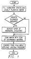
- FIG. 1 A brief flow chart of the method of the present invention is shown in Fig. 1.
- the process begins with the filling of submicron spaces with an interlevel dielectric typically comprising an oxide such as TEOS / O3 although other dielectric materials useful for filling submicron spaces can be used as well.
- the oxide is deposited using any suitable depositing method such as atmospheric or sub-atmospheric chemical vapor deposition(CVD). This will result in filling the submicron spaces in the structure resulting in an upper surface which is locally planarized.
- CVD chemical vapor deposition
- a second dielectric deposition process may be required to produce the desired dielectric thickness and to improve the global planarity.
- an etch back step may also be utilized to minimize the mirroring of underlying structure.
- the etch back and coating process may be repeated.
- the desired surface after these steps is preferably one with an aspect ratio of features of up to about 1.5/1.
- the dielectric used for local planarization should have good properties, such as having high breakdown strength, low dielectric constant, freedom from pinholes, etc, as the dielectric will become part of the final device structure.
- the global planarization is started.
- the wafer is first coated with a film of a deformable (and sacrificial) dielectric such as spun on glass(SOG), a suitable resin or even a glass.
- a deformable (and sacrificial) dielectric such as spun on glass(SOG), a suitable resin or even a glass.
- SOG spun on glass
- All of the mentioned and other useful materials for the deformable film have a characteristic, usually occurring at elevated temperatures, wherein the material is deformable under pressure.
- the uncured deformable film is applied to the wafer, it is maintained at a temperature, usually above typical room temperature, at which deformation is possible.
- the deformable film is then deformed by squeezing the film coated wafer between two ultra-parallel, ultra-flat and temperature controlled bodies.
- an ultra-flat surface is one where the maximum height variation about a mean height is in the order of about 250 A.
- Ultra-parallel implies that the two bodies between which the wafer is squeezed have surfaces which are separated by a distance which varies no more than about 250 A about the mean separation distance.
- the stress in the deformable film exceeds its yield stress, the film will deform to the shape of the plates in contact therewith.
- a pressure of up to about 2 MPa is applied during the squeezing operation, although higher pressure may be required to deform some materials.
- the temperature of the plates may be controlled to achieve a controlled curing of the deformable film.
- the temperature of the plates will be quickly raised at the beginning of the squeezing operation.
- the curing can usually be accelerated by raising the temperature. This will speed the cycle time for the manufacturing process.
- materials such as glass, they becomes deformable at elevated temperature under the applied pressure.
- the pressure may be reduced because if the rate of deformation is too great, the deformable film may crack. Also, reduced pressure may be needed to prevent squeezing most of the deformable film out from contact with one of the plates.
- the temperature of the plates can be lowered so that the wafer can be removed and a new wafer can be loaded into the squeezing apparatus.
- multiple squeeze and release cycles may be required to produce the desired conformity of the film coated surface of the wafer to the surface of the body squeezed against the film.
- an etch may be desired to reduce the thickness of the film to a desired thickness.
- Fig. 2 illustrates an apparatus for squeezing a wafer during the curing of a deformable film.
- the squeezing apparatus is located in a closed chamber 59 and includes an ultra-flat temperature controlled chuck 30 having an upper surface on which a wafer 32 rests.
- the chuck 30 has three vertical holes positioned to permit three load/unload fingers 34 to pass therethrough when desired.
- the fingers 34 are attached to a plate 36 which may be raised or lowered by any suitable mechanism in the direction of the double headed arrow 38. When the fingers 34 are in their lowered position as illustrated in Fig. 2, the wafer 32 will rest on the upper surface of the chuck 30.
- a wafer moving arm (not shown) can project through the opening 39 in the chamber 59, which is normally covered by the door 40 illustrated in its closed position, and lift the wafer 32 off the fingers 34.
- a wafer can be loaded into the assembly of Fig. 2.
- the apparatus of Fig. 2 includes a temperature controlled ultra-flat plate 42 having a lower surface preferable coated with a non-stick material 43 such as a fluro-polymer, e.g. TeflonTM, which prevents the deformable film formed on the upper surface of the wafer 32 from being separated from the wafer when pressure from the plate 42 is withdrawn.
- the plate 42 has three gimbal mounts 44 attached to the upper surface thereof.
- the gimbal mounts 44 are coupled to piezoelectric actuators 51 which are mounted on the lower surface of a plate 46 which may be rotated around the axis 47 or raised and lowered in the direction of double headed arrow 48.
- the gap between the plate 42 and the chuck 30 is monitored by three position sensors 50 (two of which are shown).
- the plate 42 in operation is lowered toward the chuck 30.
- the sensors 50 actuate the piezoelectric actuators 51 coupled thereto to adjust the squeezing pressure applied to the wafer 32 to a desired pressure.
- the above described apparatus may be utilized to produce a surface which is not flat. This is accomplished by having a desired surface topography formed on the lower surface of the plate 42.
- the plate 42 is then rotationally positioned by rotation about the axis 47 and lowered into pressure engagement with the film coated wafer. When this plate is pressed into the uncured deformable film on top of the wafer, the upper surface of the film will conform to the topography of the lower surface of the plate 42.
- Both the chuck 30 and the plate 42 are temperature controlled using conventional temperature control techniques. Both the chuck 30 and plate 42 may have resistive heating elements imbedded therein with external connections to a temperature control circuit for applying controlled electrical power to the heating elements so that chuck 30 and the plate 42 can be heated to a selected elevated temperature. In the alternative, both the chuck 30 and the plate 42 can be heated by a heated fluid which is pumped through fluid passages therein. Indeed, the chuck 30 and the plate 42 can be temperature controlled by both resistive heating elements and by heated fluid being pumped through passages therein. Other controlled heating methods and apparatus can be employed so long as a selectable temperature sufficiently high to cause the dielectric to deform under pressure can be maintained.
- the apparatus described above consists of an assembly disposed inside a closed chamber 59 largely defined by exterior walls 60.
- the door 40 illustrated in its closed position, provides access, when opened, to the closed chamber 59 through opening 39.
- a throttle valve 62 which controls the air pressure inside the chamber 59, is disposed between the chamber 59 defined by the walls 60 and a vacuum pump (not shown) which draws air out of the chamber 59 in the direction of arrow 64.
- a pressure source could be coupled to the throttle valve 62 to admit a gas into the chamber 59 at a desired pressure.
- a film of a deformable dielectric such as spun on glass (SOG) is deposited on the wafer .
- the film material can be deposited on a wafer by various methods, for example, by dripping the film material onto the wafer in a liquid state while the wafer is being spun. The material will quickly flow over the surface of the wafer.
- deformable metal films they may be deposited via sputtering or CVD and typically are selected from the group comprising aluminum, tin or other low melting point metals. At this point, the wafer is ready for the curing process during which the film is flattened.
- the wafer is placed in an apparatus of the type illustrated in Fig. 2.
- the dielectric film is deformed so as to conform to the shape of the plate 42 which is flat.
- the pressure maintained during curing is in the order of 1-10 MPa.
- the pressure maintained during curing will most likely different from that used for spun on glass and the best pressure must be determined by experimentation.
- the curing of the dielectric film is affected by temperature.
- the chuck 30 and the plate 42 in the preferred embodiment of the apparatus, are temperature controlled.
- the temperature of the chuck 30 and the plate 42 will be elevated to about 700 degrees Celsius and will be maintained at that temperature for about two (2) minutes. This elevated temperature is most easily achieved by passing a controlled current through a resistive heating element buried in the chuck 30 and the plate 42 although other approaches for heating the chuck 30 and plate 42 may also be utilized.
- the temperature is thereafter lowered using a liquid coolant which is forced through cooling passages in both the chuck 30 and the plate 42.
- the liquid coolant is utilized to rapidly cool the chuck 30 and plate 42, however, if a slower or different cooling rate is desired, other cooling methods can be used such as radiant cooling, controlled reduction of current through the resistive heating element, or any other method for achieving the desired cooling rate.
- FIG. 3 an alternative embodiment of the apparatus of Fig. 2 is shown.
- the elements of Fig. 2 which are the same as in Fig. 2 have the same lead line designations in Fig. 3 as in Fig. 2.
- the principal difference between the apparatus of Fig.2 and that of Fig. 3 is that in Fig. 2, uniform pressure on the film is provided by the plate 42 being forced into contact with the film on the wafer surface while in Fig. 3, a fluid 70 under high pressure is disposed between plate 72 and the wafer 32 to apply uniform pressure on the film on the wafer 32.
- the apparatus of Fig. 3 includes a pressure plate 72 which is movable up and down in the direction indicated by double headed arrow 74.
- the plate 72 is illustrated schematically in Fig. 3 and comprises a disc shaped body as viewed from above. Plate 72 acts like a piston and is forced downwardly by a motor or other suitable force generating apparatus (not shown) coupled to shaft 73. Downward movement of the plate 72 pressurizes the fluid 70 disposed between the plate 72 and the wafer 32. This will planarize the deformable film and also fill gaps and voids.
- the wafer 32 is maintained at suitable curing temperature by maintaining the plate 30, plate 72 and the fluid 70 at a suitable curing temperature.
- the pressure of the fluid 70 on the upper surface of the coated wafer 32 is maintained during curing in the range described with respect to the apparatus of Fig. 2.
- the fluid 70 may be either a liquid, a gas or a super critical fluid.
- a super critical fluid has properties like a gas at low pressure and properties somewhat between a gas and a liquid at high pressure.
- the fluid 70 is introduced and withdrawn from the cavity between the plate 30 and plate 72 by schematically illustrated conduits 76 and 78.
- the valve 62 and the attached pump 64 serves to evacuate any of the fluid 70 from the apparatus at times when a wafer is being either loaded or unloaded or in the event removal by the conduits 76 and 78 is not as complete as desired.
- the apparatus of Fig. 3 includes a door 80 which seals the opening 82 in the vertical wall 84 which encircles the plates 72 and 30 thereby forming the closed chamber in which the wafer 32 can be subjected to the pressurized fluid 70.
- Suitable pressure sealing rings 86 are disposed between the plate 72 and the wall 84 to prevent the fluid 70, when under pressure, from escaping from the chamber formed between the wall 84 and plates 30 and 72.
- Suitable additional sealing rings may be required between the plate 30 and the wall 84 if it is desired not to fill the chamber 88 located below the plate 30 and the exterior wall 90 of the apparatus. In this alternative, seals may also be required between the posts 34 and the plate 30.
- the wafer 32 is loaded and unloaded from the apparatus of Fig. 3 in a manner similar to that of Fig. 2.
- the atmosphere within the apparatus is first adjusted to that of the environment outside door 40.
- both door 40 and door 80 are opened.
- the posts 34 are raised to lift the wafer 32 above the plate 30 and an external arm (not shown) enters the chamber and lifts the wafer 32 off the posts 34.
- the wafer 32 is withdrawn and another introduced for planarization.
Landscapes
- Engineering & Computer Science (AREA)
- Mechanical Engineering (AREA)
- Internal Circuitry In Semiconductor Integrated Circuit Devices (AREA)
- Formation Of Insulating Films (AREA)
Applications Claiming Priority (2)
| Application Number | Priority Date | Filing Date | Title |
|---|---|---|---|
| US188498 | 1994-01-28 | ||
| US08/188,498 US5434107A (en) | 1994-01-28 | 1994-01-28 | Method for planarization |
Publications (2)
| Publication Number | Publication Date |
|---|---|
| EP0665580A2 true EP0665580A2 (fr) | 1995-08-02 |
| EP0665580A3 EP0665580A3 (fr) | 1997-03-05 |
Family
ID=22693403
Family Applications (1)
| Application Number | Title | Priority Date | Filing Date |
|---|---|---|---|
| EP95100971A Withdrawn EP0665580A3 (fr) | 1994-01-28 | 1995-01-25 | Méthode et dispositif pour la planarisation globale de la surface d'un substrat semi-conducteur. |
Country Status (5)
| Country | Link |
|---|---|
| US (1) | US5434107A (fr) |
| EP (1) | EP0665580A3 (fr) |
| JP (1) | JPH0817812A (fr) |
| KR (1) | KR950034586A (fr) |
| TW (1) | TW299483B (fr) |
Cited By (3)
| Publication number | Priority date | Publication date | Assignee | Title |
|---|---|---|---|---|
| EP1440465A4 (fr) * | 2001-10-31 | 2010-08-25 | Brewer Science Inc | Des materiaux de planarisation par contact qui ne generent pas de sous-produits ou de residus volatiles pendant le durcissement |
| EP3637456A3 (fr) * | 2018-10-11 | 2020-12-16 | Canon Kabushiki Kaisha | Appareil de formation de film, procédé de formation de film et procédé de fabrication d'article |
| KR20210148328A (ko) * | 2019-05-07 | 2021-12-07 | 에이에스엠엘 홀딩 엔.브이. | 리소그래피 장치, 기판 테이블, 및 불균일 코팅 방법 |
Families Citing this family (78)
| Publication number | Priority date | Publication date | Assignee | Title |
|---|---|---|---|---|
| US5736424A (en) * | 1987-02-27 | 1998-04-07 | Lucent Technologies Inc. | Device fabrication involving planarization |
| US5679610A (en) * | 1994-12-15 | 1997-10-21 | Kabushiki Kaisha Toshiba | Method of planarizing a semiconductor workpiece surface |
| TW291589B (fr) * | 1995-03-30 | 1996-11-21 | Ftl Co Ltd | |
| US5679211A (en) * | 1995-09-18 | 1997-10-21 | Taiwan Semiconductor Manufacturing Company, Ltd. | Spin-on-glass etchback planarization process using an oxygen plasma to remove an etchback polymer residue |
| US7758794B2 (en) * | 2001-10-29 | 2010-07-20 | Princeton University | Method of making an article comprising nanoscale patterns with reduced edge roughness |
| US20040137734A1 (en) * | 1995-11-15 | 2004-07-15 | Princeton University | Compositions and processes for nanoimprinting |
| US6518189B1 (en) * | 1995-11-15 | 2003-02-11 | Regents Of The University Of Minnesota | Method and apparatus for high density nanostructures |
| US20040036201A1 (en) * | 2000-07-18 | 2004-02-26 | Princeton University | Methods and apparatus of field-induced pressure imprint lithography |
| US6309580B1 (en) * | 1995-11-15 | 2001-10-30 | Regents Of The University Of Minnesota | Release surfaces, particularly for use in nanoimprint lithography |
| US5967030A (en) | 1995-11-17 | 1999-10-19 | Micron Technology, Inc. | Global planarization method and apparatus |
| US6413870B1 (en) | 1996-09-30 | 2002-07-02 | International Business Machines Corporation | Process of removing CMP scratches by BPSG reflow and integrated circuit chip formed thereby |
| US5848615A (en) * | 1996-12-04 | 1998-12-15 | Ingersoll-Rand Company | Check valve cartridge for fluid pump |
| US6316363B1 (en) | 1999-09-02 | 2001-11-13 | Micron Technology, Inc. | Deadhesion method and mechanism for wafer processing |
| US6331488B1 (en) * | 1997-05-23 | 2001-12-18 | Micron Technology, Inc. | Planarization process for semiconductor substrates |
| GB9714531D0 (en) * | 1997-07-11 | 1997-09-17 | Trikon Equip Ltd | Forming a layer |
| US6060386A (en) * | 1997-08-21 | 2000-05-09 | Micron Technology, Inc. | Method and apparatus for forming features in holes, trenches and other voids in the manufacturing of microelectronic devices |
| US6103638A (en) | 1997-11-07 | 2000-08-15 | Micron Technology, Inc. | Formation of planar dielectric layers using liquid interfaces |
| EP0948035A1 (fr) * | 1998-03-19 | 1999-10-06 | Applied Materials, Inc. | Méthode d'application d'un film diélectrique de recouvrement sur un empilement diélectrique |
| US6036586A (en) * | 1998-07-29 | 2000-03-14 | Micron Technology, Inc. | Apparatus and method for reducing removal forces for CMP pads |
| CA2342332A1 (fr) * | 1998-08-31 | 2000-03-09 | Hiroki Terazaki | Liquide abrasif pour le polissage de metaux et procede correspondant |
| US6333264B1 (en) | 1998-09-02 | 2001-12-25 | Micron Technology, Inc. | Semiconductor processing method using high pressure liquid media treatment |
| US6642140B1 (en) | 1998-09-03 | 2003-11-04 | Micron Technology, Inc. | System for filling openings in semiconductor products |
| US6218316B1 (en) | 1998-10-22 | 2001-04-17 | Micron Technology, Inc. | Planarization of non-planar surfaces in device fabrication |
| JP3832142B2 (ja) | 1999-06-24 | 2006-10-11 | 株式会社日立製作所 | 配管系の減肉管理システム |
| US6589889B2 (en) * | 1999-09-09 | 2003-07-08 | Alliedsignal Inc. | Contact planarization using nanoporous silica materials |
| AU7367400A (en) * | 1999-09-09 | 2001-04-10 | Allied-Signal Inc. | Improved apparatus and methods for integrated circuit planarization |
| US6165911A (en) * | 1999-12-29 | 2000-12-26 | Calveley; Peter Braden | Method of patterning a metal layer |
| DE10022656B4 (de) * | 2000-04-28 | 2006-07-06 | Infineon Technologies Ag | Verfahren zum Entfernen von Strukturen |
| US7211214B2 (en) * | 2000-07-18 | 2007-05-01 | Princeton University | Laser assisted direct imprint lithography |
| AU2001290171A1 (en) * | 2000-07-26 | 2002-02-05 | Tokyo Electron Limited | High pressure processing chamber for semiconductor substrate |
| US6518172B1 (en) | 2000-08-29 | 2003-02-11 | Micron Technology, Inc. | Method for applying uniform pressurized film across wafer |
| JP3927768B2 (ja) * | 2000-11-17 | 2007-06-13 | 松下電器産業株式会社 | 半導体装置の製造方法 |
| US20020164875A1 (en) * | 2001-05-04 | 2002-11-07 | Leong Lup San | Thermal mechanical planarization in integrated circuits |
| US20030080472A1 (en) * | 2001-10-29 | 2003-05-01 | Chou Stephen Y. | Lithographic method with bonded release layer for molding small patterns |
| US7455955B2 (en) * | 2002-02-27 | 2008-11-25 | Brewer Science Inc. | Planarization method for multi-layer lithography processing |
| US7387868B2 (en) * | 2002-03-04 | 2008-06-17 | Tokyo Electron Limited | Treatment of a dielectric layer using supercritical CO2 |
| US7077992B2 (en) | 2002-07-11 | 2006-07-18 | Molecular Imprints, Inc. | Step and repeat imprint lithography processes |
| US6932934B2 (en) | 2002-07-11 | 2005-08-23 | Molecular Imprints, Inc. | Formation of discontinuous films during an imprint lithography process |
| US8349241B2 (en) | 2002-10-04 | 2013-01-08 | Molecular Imprints, Inc. | Method to arrange features on a substrate to replicate features having minimal dimensional variability |
| US7225820B2 (en) * | 2003-02-10 | 2007-06-05 | Tokyo Electron Limited | High-pressure processing chamber for a semiconductor wafer |
| US7186656B2 (en) * | 2004-05-21 | 2007-03-06 | Molecular Imprints, Inc. | Method of forming a recessed structure employing a reverse tone process |
| US7179396B2 (en) | 2003-03-25 | 2007-02-20 | Molecular Imprints, Inc. | Positive tone bi-layer imprint lithography method |
| US7323417B2 (en) * | 2004-09-21 | 2008-01-29 | Molecular Imprints, Inc. | Method of forming a recessed structure employing a reverse tone process |
| US7396475B2 (en) | 2003-04-25 | 2008-07-08 | Molecular Imprints, Inc. | Method of forming stepped structures employing imprint lithography |
| US7270137B2 (en) | 2003-04-28 | 2007-09-18 | Tokyo Electron Limited | Apparatus and method of securing a workpiece during high-pressure processing |
| US7790231B2 (en) * | 2003-07-10 | 2010-09-07 | Brewer Science Inc. | Automated process and apparatus for planarization of topographical surfaces |
| US7163380B2 (en) * | 2003-07-29 | 2007-01-16 | Tokyo Electron Limited | Control of fluid flow in the processing of an object with a fluid |
| US20050067002A1 (en) * | 2003-09-25 | 2005-03-31 | Supercritical Systems, Inc. | Processing chamber including a circulation loop integrally formed in a chamber housing |
| US7041604B2 (en) * | 2004-09-21 | 2006-05-09 | Molecular Imprints, Inc. | Method of patterning surfaces while providing greater control of recess anisotropy |
| US7252777B2 (en) * | 2004-09-21 | 2007-08-07 | Molecular Imprints, Inc. | Method of forming an in-situ recessed structure |
| US7205244B2 (en) * | 2004-09-21 | 2007-04-17 | Molecular Imprints | Patterning substrates employing multi-film layers defining etch-differential interfaces |
| US7547504B2 (en) | 2004-09-21 | 2009-06-16 | Molecular Imprints, Inc. | Pattern reversal employing thick residual layers |
| US7241395B2 (en) * | 2004-09-21 | 2007-07-10 | Molecular Imprints, Inc. | Reverse tone patterning on surfaces having planarity perturbations |
| US20060102282A1 (en) * | 2004-11-15 | 2006-05-18 | Supercritical Systems, Inc. | Method and apparatus for selectively filtering residue from a processing chamber |
| WO2006060757A2 (fr) * | 2004-12-01 | 2006-06-08 | Molecular Imprints, Inc. | Elimination de l'imprimabilite de defauts de sous-resolution dans la lithographie par impression |
| US7767145B2 (en) * | 2005-03-28 | 2010-08-03 | Toyko Electron Limited | High pressure fourier transform infrared cell |
| US20060225772A1 (en) * | 2005-03-29 | 2006-10-12 | Jones William D | Controlled pressure differential in a high-pressure processing chamber |
| US20060226117A1 (en) * | 2005-03-29 | 2006-10-12 | Bertram Ronald T | Phase change based heating element system and method |
| US7494107B2 (en) * | 2005-03-30 | 2009-02-24 | Supercritical Systems, Inc. | Gate valve for plus-atmospheric pressure semiconductor process vessels |
| US20060225769A1 (en) * | 2005-03-30 | 2006-10-12 | Gentaro Goshi | Isothermal control of a process chamber |
| US7256131B2 (en) * | 2005-07-19 | 2007-08-14 | Molecular Imprints, Inc. | Method of controlling the critical dimension of structures formed on a substrate |
| US20070077763A1 (en) * | 2005-09-30 | 2007-04-05 | Molecular Imprints, Inc. | Deposition technique to planarize a multi-layer structure |
| US7803308B2 (en) | 2005-12-01 | 2010-09-28 | Molecular Imprints, Inc. | Technique for separating a mold from solidified imprinting material |
| US7906058B2 (en) * | 2005-12-01 | 2011-03-15 | Molecular Imprints, Inc. | Bifurcated contact printing technique |
| US7670530B2 (en) | 2006-01-20 | 2010-03-02 | Molecular Imprints, Inc. | Patterning substrates employing multiple chucks |
| MY144847A (en) | 2005-12-08 | 2011-11-30 | Molecular Imprints Inc | Method and system for double-sided patterning of substrates |
| US7802978B2 (en) | 2006-04-03 | 2010-09-28 | Molecular Imprints, Inc. | Imprinting of partial fields at the edge of the wafer |
| US8850980B2 (en) | 2006-04-03 | 2014-10-07 | Canon Nanotechnologies, Inc. | Tessellated patterns in imprint lithography |
| US8142850B2 (en) | 2006-04-03 | 2012-03-27 | Molecular Imprints, Inc. | Patterning a plurality of fields on a substrate to compensate for differing evaporation times |
| US7780893B2 (en) * | 2006-04-03 | 2010-08-24 | Molecular Imprints, Inc. | Method of concurrently patterning a substrate having a plurality of fields and a plurality of alignment marks |
| US7547398B2 (en) | 2006-04-18 | 2009-06-16 | Molecular Imprints, Inc. | Self-aligned process for fabricating imprint templates containing variously etched features |
| US8012395B2 (en) | 2006-04-18 | 2011-09-06 | Molecular Imprints, Inc. | Template having alignment marks formed of contrast material |
| US7775785B2 (en) * | 2006-12-20 | 2010-08-17 | Brewer Science Inc. | Contact planarization apparatus |
| JP4754595B2 (ja) * | 2008-03-05 | 2011-08-24 | 大日本スクリーン製造株式会社 | 薄膜形成装置および方法 |
| US8865599B2 (en) * | 2011-11-08 | 2014-10-21 | Brewer Science Inc. | Self-leveling planarization materials for microelectronic topography |
| JP2013163846A (ja) * | 2012-02-10 | 2013-08-22 | Denso Corp | 成膜装置及び成膜方法 |
| TWM473078U (zh) | 2013-10-07 | 2014-03-01 | Lin Chen Ind Co Ltd | 以相同布材縫製的褲子 |
| JP7129315B2 (ja) * | 2018-11-05 | 2022-09-01 | キヤノン株式会社 | 平坦化層形成装置、平坦化方法、および、物品製造方法 |
Family Cites Families (12)
| Publication number | Priority date | Publication date | Assignee | Title |
|---|---|---|---|---|
| WO1993013557A1 (fr) * | 1985-02-14 | 1993-07-08 | Yoshiyuki Sato | Structure de montage tridimensionnel de puces a semi-conducteurs |
| JPS6245045A (ja) * | 1985-08-22 | 1987-02-27 | Nec Corp | 半導体装置の製造方法 |
| JPS6245032A (ja) * | 1985-08-22 | 1987-02-27 | Nec Corp | 半導体装置の製造方法 |
| GB2212332A (en) * | 1987-11-11 | 1989-07-19 | Gen Electric Co Plc | Fabrication of electrical circuits |
| EP0430040A3 (en) * | 1989-11-27 | 1992-05-20 | Micron Technology, Inc. | Method of forming a conductive via plug or an interconnect line of ductile metal within an integrated circuit using mechanical smearing |
| US5073518A (en) * | 1989-11-27 | 1991-12-17 | Micron Technology, Inc. | Process to mechanically and plastically deform solid ductile metal to fill contacts of conductive channels with ductile metal and process for dry polishing excess metal from a semiconductor wafer |
| EP0526889B1 (fr) * | 1991-08-06 | 1997-05-07 | Nec Corporation | Procédé de dépÔt d'un film métallique ou de passivation à haute adhérence sur un substrat semi-conducteur isolé |
| JP3233664B2 (ja) * | 1991-09-13 | 2001-11-26 | 土肥 俊郎 | デバイス付きウェーハのプラナリゼーションポリッシング方法及びその装置 |
| US5326243A (en) * | 1992-06-25 | 1994-07-05 | Fierkens Richard H J | Compression-cavity mold for plastic encapsulation of thin-package integrated circuit device |
| US5348615A (en) * | 1992-10-21 | 1994-09-20 | Advanced Micro Devices, Inc. | Selective planarization method using regelation |
| US5302233A (en) * | 1993-03-19 | 1994-04-12 | Micron Semiconductor, Inc. | Method for shaping features of a semiconductor structure using chemical mechanical planarization (CMP) |
| GB9321900D0 (en) * | 1993-10-23 | 1993-12-15 | Dobson Christopher D | Method and apparatus for the treatment of semiconductor substrates |
-
1994
- 1994-01-28 US US08/188,498 patent/US5434107A/en not_active Expired - Lifetime
-
1995
- 1995-01-25 EP EP95100971A patent/EP0665580A3/fr not_active Withdrawn
- 1995-01-27 KR KR1019950001501A patent/KR950034586A/ko not_active Ceased
- 1995-01-30 JP JP7013038A patent/JPH0817812A/ja active Pending
- 1995-03-09 TW TW084102223A patent/TW299483B/zh not_active IP Right Cessation
Cited By (4)
| Publication number | Priority date | Publication date | Assignee | Title |
|---|---|---|---|---|
| EP1440465A4 (fr) * | 2001-10-31 | 2010-08-25 | Brewer Science Inc | Des materiaux de planarisation par contact qui ne generent pas de sous-produits ou de residus volatiles pendant le durcissement |
| EP3637456A3 (fr) * | 2018-10-11 | 2020-12-16 | Canon Kabushiki Kaisha | Appareil de formation de film, procédé de formation de film et procédé de fabrication d'article |
| US11275309B2 (en) | 2018-10-11 | 2022-03-15 | Canon Kabushiki Kaisha | Film forming apparatus, film forming method, and method of manufacturing article |
| KR20210148328A (ko) * | 2019-05-07 | 2021-12-07 | 에이에스엠엘 홀딩 엔.브이. | 리소그래피 장치, 기판 테이블, 및 불균일 코팅 방법 |
Also Published As
| Publication number | Publication date |
|---|---|
| TW299483B (fr) | 1997-03-01 |
| EP0665580A3 (fr) | 1997-03-05 |
| US5434107A (en) | 1995-07-18 |
| JPH0817812A (ja) | 1996-01-19 |
| KR950034586A (ko) | 1995-12-28 |
Similar Documents
| Publication | Publication Date | Title |
|---|---|---|
| US5434107A (en) | Method for planarization | |
| US5516729A (en) | Method for planarizing a semiconductor topography using a spin-on glass material with a variable chemical-mechanical polish rate | |
| US6653722B2 (en) | Method for applying uniform pressurized film across wafer | |
| US6683003B2 (en) | Global planarization method and apparatus | |
| US6407009B1 (en) | Methods of manufacture of uniform spin-on films | |
| US6331488B1 (en) | Planarization process for semiconductor substrates | |
| US4806504A (en) | Planarization method | |
| US7947603B2 (en) | Chemical-mechanical polishing method | |
| KR100434929B1 (ko) | 공극이없는연속평탄화기판표면형성방법 | |
| US5106787A (en) | Method for high vacuum controlled ramping curing furnace for SOG planarization | |
| EP0386337A2 (fr) | Procédé de dépôt en phase vapeur planarisé à plusieurs étapes | |
| US6530340B2 (en) | Apparatus for manufacturing planar spin-on films | |
| US6103638A (en) | Formation of planar dielectric layers using liquid interfaces | |
| US6225240B1 (en) | Rapid acceleration methods for global planarization of spin-on films | |
| US6317642B1 (en) | Apparatus and methods for uniform scan dispensing of spin-on materials | |
| US6387825B2 (en) | Solution flow-in for uniform deposition of spin-on films | |
| US6693034B2 (en) | Deadhesion method and mechanism for wafer processing | |
| EP0498521B1 (fr) | Procédé pour planariser une surface de dispositif à circuit intégré | |
| US5174043A (en) | Machine and method for high vacuum controlled ramping curing furnace for sog planarization | |
| US20150206794A1 (en) | Method for Removing Micro Scratches In Chemical Mechanical Polishing Processes | |
| Sato et al. | Advanced transfer system for spin coating film transfer and hot-pressing in planarization technology | |
| EP1254742A2 (fr) | Planarisation mécano-thermique de circuits intégrés | |
| US20020146896A1 (en) | Metallizaton methods using foils | |
| JP2005101036A (ja) | 半導体素子の製造方法 | |
| JPH09260377A (ja) | 半導体装置の製造方法 |
Legal Events
| Date | Code | Title | Description |
|---|---|---|---|
| PUAI | Public reference made under article 153(3) epc to a published international application that has entered the european phase |
Free format text: ORIGINAL CODE: 0009012 |
|
| AK | Designated contracting states |
Kind code of ref document: A2 Designated state(s): DE FR GB IT NL |
|
| PUAL | Search report despatched |
Free format text: ORIGINAL CODE: 0009013 |
|
| RHK1 | Main classification (correction) |
Ipc: H01L 21/3105 |
|
| AK | Designated contracting states |
Kind code of ref document: A3 Designated state(s): DE FR GB IT NL |
|
| 17P | Request for examination filed |
Effective date: 19970904 |
|
| STAA | Information on the status of an ep patent application or granted ep patent |
Free format text: STATUS: THE APPLICATION IS DEEMED TO BE WITHDRAWN |
|
| 18D | Application deemed to be withdrawn |
Effective date: 20060624 |