EP0665633A2 - Conversion de puissance - Google Patents
Conversion de puissance Download PDFInfo
- Publication number
- EP0665633A2 EP0665633A2 EP95300412A EP95300412A EP0665633A2 EP 0665633 A2 EP0665633 A2 EP 0665633A2 EP 95300412 A EP95300412 A EP 95300412A EP 95300412 A EP95300412 A EP 95300412A EP 0665633 A2 EP0665633 A2 EP 0665633A2
- Authority
- EP
- European Patent Office
- Prior art keywords
- switching device
- capacitance
- circuit
- converter
- current
- Prior art date
- Legal status (The legal status is an assumption and is not a legal conclusion. Google has not performed a legal analysis and makes no representation as to the accuracy of the status listed.)
- Granted
Links
Images















Classifications
-
- H—ELECTRICITY
- H02—GENERATION; CONVERSION OR DISTRIBUTION OF ELECTRIC POWER
- H02M—APPARATUS FOR CONVERSION BETWEEN AC AND AC, BETWEEN AC AND DC, OR BETWEEN DC AND DC, AND FOR USE WITH MAINS OR SIMILAR POWER SUPPLY SYSTEMS; CONVERSION OF DC OR AC INPUT POWER INTO SURGE OUTPUT POWER; CONTROL OR REGULATION THEREOF
- H02M3/00—Conversion of DC power input into DC power output
- H02M3/22—Conversion of DC power input into DC power output with intermediate conversion into AC
- H02M3/24—Conversion of DC power input into DC power output with intermediate conversion into AC by static converters
- H02M3/28—Conversion of DC power input into DC power output with intermediate conversion into AC by static converters using discharge tubes with control electrode or semiconductor devices with control electrode to produce the intermediate AC
- H02M3/325—Conversion of DC power input into DC power output with intermediate conversion into AC by static converters using discharge tubes with control electrode or semiconductor devices with control electrode to produce the intermediate AC using devices of a triode or a transistor type requiring continuous application of a control signal
- H02M3/335—Conversion of DC power input into DC power output with intermediate conversion into AC by static converters using discharge tubes with control electrode or semiconductor devices with control electrode to produce the intermediate AC using devices of a triode or a transistor type requiring continuous application of a control signal using semiconductor devices only
- H02M3/33569—Conversion of DC power input into DC power output with intermediate conversion into AC by static converters using discharge tubes with control electrode or semiconductor devices with control electrode to produce the intermediate AC using devices of a triode or a transistor type requiring continuous application of a control signal using semiconductor devices only having several active switching elements
- H02M3/33576—Conversion of DC power input into DC power output with intermediate conversion into AC by static converters using discharge tubes with control electrode or semiconductor devices with control electrode to produce the intermediate AC using devices of a triode or a transistor type requiring continuous application of a control signal using semiconductor devices only having several active switching elements having at least one active switching element at the secondary side of an isolation transformer
Definitions
- This invention relates to power conversion circuits.
- Figure 1 shows a zero-current switching forward converter 10 of the kind described in Vinciarelli, "Forward Converter Switching at Zero-Current," U.S. Patent 4,415,959 (incorporated by reference).
- a finite and bounded amount (quantum) of energy is transferred from the input source 12 to the load 200 during each converter operating cycle.
- the amount of power delivered to the load is a function of converter operating frequency (i.e., the number of operating cycles per second).
- control circuits 22 are used both to turn the main switch 26 on and off at times of zero current and to vary the converter operating frequency as the power drawn by the external load 200 varies.
- a zero-current switching converter it is beneficial to reduce the operating frequency range of a zero-current switching converter by raising its minimum operating frequency. For example, increasing the minimum operating frequency allows use of smaller valued converter output filter elements. This allows reducing the physical size and losses in these elements and also provides for wider closed-loop converter operating bandwidths and improved converter response times. Similarly, an increased minimum operating frequency allows use of smaller input filtering elements, for reducing the levels of the frequency components reflected back toward the input source, with similar benefits.
- One way of raising the minimum operating frequency in a zero-current switching converter is to provide means for reducing the amount of energy transferred to the load during each energy transfer cycle.
- One way of accomplishing this is described in Vinciarelli, "Zero Current Switching Forward Power Conversion Apparatus and Method With Controllable Energy Transfer," U.S. Patent 5,235,502, incorporated by reference.
- the converter described therein, and shown as converter 50 in Figure 2 incorporates a bidirectional switching element 28 which is turned on and off in synchronism with the main switch in an operating mode called the reverse boost operating mode.
- a reverse boost controller 32 turns the bidirectional switch 28 off when the main switch 26 is turned on (thereby enabling forward energy transfer to take place from the input source to the capacitor 20 and thence to the load 200) and turns the bidirectional switch on later in the operating cycle when the capacitor 20 voltage returns to zero.
- the operation of the converter of Figure 2 is substantially identical to the operation of the converter of Figure 1.
- the closed bidirectional switch will conduct the reverse current around the capacitor, thereby preventing uncontrolled charging.
- bidirectional switch and output filter capacitors e.g., capacitor 201 in Figure 2
- ripple voltage due both to integrating effect of the output capacitance and to the effect of current flow in the equivalent series impedances of the nonideal output filter capacitors
- a reverse boost controller 32 synchronizes the opening and closing of the bidirectional switch with the opening and closing of the main switch using the same protocol described above for the converter of Figure 2 operating in reverse boost mode.
- the dissipative element acts to limit the peak (and hence the initial) value of reverse current and, in doing so, also acts to dissipate some power.
- the combined effect is a reduction in forward energy transfer at light or zero loads and an increase in minimum operating frequency owing to both the reduction in forward energy transfer and the losses in the resistive element.
- the converter of Figure 3 When operated in this "damped reverse boost" mode of operation, the converter of Figure 3 avoids the higher initial values of reverse current associated with the reverse boost operating mode in the converter of Figure 2 and eliminates the discontinuous operating mode, but does so at the expense of increased dissipation, and wasted power, in the dissipative element 210.
- Both the reverse boost and the damped reverse boost operating modes exploit current reversal in the output inductor at light loads as a means of supplying a portion of the total energy delivered to the capacitor 20.
- This "reverse" energy transfer acts in natural opposition to "forward” transfer of energy to the capacitor from the input source.
- the "reverse” energy transfer process is initiated concurrently with initiation of forward energy transfer (i.e., the bidirectional switches 28, 252 are opened by the reverse boost controller at essentially the same time that the main switches 26 are closed). With this switching protocol, reverse current flow can decrease forward energy transfer but it cannot reduce it to zero, as this would require an infinite initial value of reverse current.
- the minimum operating frequency for each of the converters of Figures 2 and 3 is higher than the average minimum operating frequency for the converter of Figure 1 because of the reduction in forward energy transfer at low values of load brought about by the aforementioned reverse boost operating modes.
- the minimum operating frequency is primarily dependent upon losses in nonideal or dissipative components within the converter.
- the invention features a power conversion circuit having a port for connection to a power source; a transformer having a primary winding, a secondary winding, and an effective secondary leakage inductance L2e; and a capacitance C connected on a secondary side of the transformer.
- a first switching device is connected to be opened and closed to transfer energy from the power source via the effective leakage inductance to charge the capacitance during a forward energy transfer cycle having a characteristic time scale of pi*sqrt(L2e*C).
- There is control circuitry connected to control precharging of the capacitance at selected times other than during the forward energy transfer cycle.
- Embodiments of the invention may include one or more of the following features.
- the control circuitry is configured to govern the times of precharging relative to the onset of the forward energy transfer cycle.
- the control circuitry includes a second switching device. Precharging is begun by opening the second switching device.
- a load is connected to receive energy from the capacitance.
- An inductor is connected to carry current between the capacitance and the load.
- the second switching device is connected in parallel with the capacitance and in series with the inductor.
- a unidirectional conducting device is connected in series with the secondary winding and oriented to conduct during conduction by the first switching device.
- the control circuitry includes a port for receiving a signal indicative of a rate of change of voltage across the capacitance, and a port for receiving a signal indicative of a frequency of operation of the circuit, and those signals are used in controlling the precharging.
- the second switching device is an essentially lossless switch. In some embodiments the second switching device has finite resistance.
- the second switching device may include a switch and a finite resistance external to the switch.
- the second switching device may be a MOSFET.
- a unidirectional conducting device may be connected across the second switching device and poled to conduct current in the direction of the load (e.g., in a direction opposite to the direction of conduction of the MOSFET).
- the circuit may be operated in a mode having a conversion operating cycle of which the forward energy transfer cycle is a portion, and where the conversion operating cycle includes another portion in which reverse current flowing from the load is available to charge the capacitance, the reverse current being routed to the capacitor to achieve precharging.
- the first switching device is turned on and turned off at times when current through the first switching device is essentially zero.
- the frequency of switching of the first switching device is controlled to maintain an output voltage of the circuit at a predetermined value.
- a condition for turning on the second switching device is approximately an occurrence of a time when a voltage across the capacitor is essentially zero.
- the second switching device is turned off approximately at a time such that the subsequent forward energy transfer cycle will tend to begin when a voltage across the capacitor is at a maximum.
- the time occurs briefly prior to when the voltage across the capacitor is maximum.
- the maximum comprises the first maximum to occur following the time when the second switching device is turned off.
- the precharging is disabled in periods when the reverse current does not flow during the conversion operating cycle.
- Fig. 1 shows a schematic diagram of a zero-current switching converter.
- Fig. 2 shows a schematic diagram of a zero-current switching DC-DC converter which includes circuit and control elements for operating the converter in a reverse boost mode of operation.
- Fig. 3 shows a schematic diagram of a zero-current switching DC-DC converter which includes circuit and control elements for operating the converter in a damped reverse boost mode of operation.
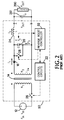
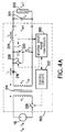
- Figs. 4A and 4B show schematic diagrams for isolated and non-isolated embodiments of a zero-current switching DC-DC converter which includes a controller for operating the converter in an anticipatory reverse boost mode of operation.
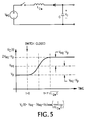
- Fig. 5 illustrates a circuit and the effect of the presence of a precharge voltage on the peak voltage to which a capacitor will be charged in the circuit.
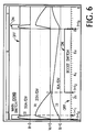
- Fig. 6 shows waveforms for a converter of the kind shown in Figs. 4A and 4B when the converter is delivering a sufficient amount of power to a load such that current reversal in the converter output inductor does not occur.
- Figs. 7 - 10 shows waveforms for a converter of the kind shown in Figs. 4A and 4B when the converter is delivering relatively low values of load power for which current reversal occurs in the converter output inductor.
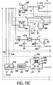
- Fig. 11 shows a schematic diagram of an embodiment of an anticipatory reverse boost DC-DC converter which includes a schematic diagram of a reverse boost phase controller.
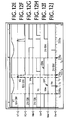
- Figs. 12A - 12N show operating waveforms for the converter of Fig. 11 operating at essentially zero load conditions.
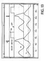
- Fig. 13 shows an alternate operating mode which is avoided by means of circuitry included in the converter of Fig. 11.
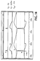
- Figs. 14 - 16 show operating waveforms for the converter of Figure 11 under various load conditions.
- Figs. 17A and 17B show schematic diagrams for isolated and non-isolated embodiments of a zero-current switching DC-DC converter which includes a controller for operating the converter in a damped anticipatory reverse boost mode of operation.
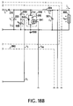
- Fig. 18 shows a schematic diagram of an embodiment of a damped anticipatory reverse boost DC-DC converter which includes a schematic diagram of a reverse boost phase controller.
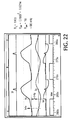
- Fig. 19 - 22 show operating waveforms for the converter of Figure 18 under various load conditions.
- Fig. 23 shows a table comparing the performance of four kinds of converters.
- FIG. 4A An improved zero-current switching converter, which can be operated in a mode which improves upon the performance of the reverse boost and damped reverse boost operating modes, is illustrated in Figures 4A and 4B.
- the converter accepts power from an input voltage source 112, of value Vin, and delivers power to an external load 300 in a series of forward energy transfer cycles.
- An output filter capacitor 301 is shown connected across the external load.
- the converter of Figure 4A differs from the converter of Figure 2 in that the reverse boost controller 32 of Figure 2 has been replaced with a new controller called a reverse boost phase controller 360.
- Figure 4B is also representative of a non-isolated version of the converter of Figure 4A, where the inductor 114 and the input source 312 are not equivalent circuit values but are actual circuit components. The discussion which follows applies to both the converter of Figure 4A and the converter of Figure 4B.
- the operation of the converter of Figure 4A is based in the principle that if the capacitor 220 is precharged to a voltage, Vp, at the time that a forward energy transfer cycle is initiated (e.g., when the main switch 226 is closed), then the energy transferred forward from the input source to the capacitor will be reduced relative to the amount of energy which would otherwise be transferred forward if Vp were zero.
- the principle is illustrated in Figure 5, which shows a circuit model consisting of an input source, of value Veq, an inductance, of value L2e, a capacitor, of value C, a switch and a diode (which are representative of the circuit elements within the zero-current switching converters of Figures 1, 2, 3, or 4 associated with forward energy transfer).
- Vp the voltage
- Vp the precharge voltage
- Veq the secondary-reflected input voltage
- a reverse boost phase controller 360 which can control the timing of the opening of the boost switch 228 to occur in anticipation of the closing of the main switch 226 during each converter operating cycle.
- opening the boost switch prior to closing the main switch will cause energy stored in the output inductor to precharge the capacitor 220. This precharge will then reduce the energy transferred forward when the main switch is subsequently closed.
- the reverse boost phase controller 360 of Fig. 4 differs from the reverse boost controllers 32 of Figs.
- the converter of Figure 4A includes two controllers: control circuits 222 and the reverse boost phase controller 360.
- Control circuits 222 are of the kind which turn the main switch 226 on and off (at times of zero current) at a converter operating frequency which is consistent with maintaining the converter output voltage Vout at some predetermined value.
- Feedback controllers of this type are well known in the art (see, for example, Vinciarelli, U.S. Patent 4,415,959 and EP-A-0 564 289 of VLT Corporation).
- the reverse boost phase controller 360 (which will be referred to as the "phase controller") controls the timing of the opening of the boost switch 228 during an operating cycle relative to the closing of the main switch 226.
- the phase controller 360 opens and closes the boost switch using the same switching protocol used by the reverse boost controllers 32 of Figures 2 and 3.
- operation of the converter of Figure 4A is substantially identical to the converters of Figures 1, 2 and 3.
- the phase controller 360 of Figure 4A adjusts the timing of the opening the boost switch to occur in anticipation of the closing of the main switch.
- the control objective chosen for the reverse boost phase controller 360 is one which seeks to optimally exploit reverse current flow at low values of load so as to maximize the operating frequency of the converter under conditions of zero load.
- the control strategy involves using the "phase controller” 360 to control the time at which the boost switch is opened such that subsequent closure of the main switch (by the "frequency controller” 222) occurs when the "precharge" voltage induced on the capacitor by current reversal in the output inductor is at a maximum.
- Figure 6 shows waveforms for the converter under a light load condition (22 Watts) for which current in the output inductor closely approaches zero but for which current reversal does not occur.
- phase controller 360 asserts no direct control over the phase of the opening of the boost switch relative to the main switch; rather it always opens it at "zero phase” (e.g., at essentially the same time that the main switch is closed). Only “frequency control” is asserted under these conditions (by control circuits 222) as a means of maintaining the output voltage at the desired, predetermined, value.
- Figures 8, 9 and 10 show additional sets of operating waveforms which, when compared with Figure 7, indicate how the converter responds to further reductions in converter load.
- the converter loading is 6.3 Watts, 5.3 Watts, 2.84 Watts and 0.053 Watts, respectively.
- the peak current in the output inductor at zero load is a relatively modest 3 Amperes. This is substantially less than the values of peak currents which are exhibited in a converter of the kind shown in Figure 2 operating in reverse boost mode.
- Figure 11 shows a schematic diagram of a DC-DC converter 650 which includes both reverse boost phase controller circuitry 360, suitable for implementing the reverse boost control strategy described above, and control circuits 222 of the kind which turn the main switch 226 on and off (at times of zero current) at a converter operating frequency which is consistent with maintaining the converter output voltage at some predetermined value.
- the converter includes primary-to-secondary isolation (i.e., power conversion circuitry includes an isolation transformer, as in Figure 4A, and any circuitry which is electrically connected to the input voltage source 112 is galvanically isolated from circuitry connected to the load, as indicated by the two different return reference symbols 697, 699 used in Figure 11) but it should be apparent that the same operating principles would apply to a non-isolated converter (e.g., of the kind shown in Figure 4B).
- power conversion circuitry includes an isolation transformer, as in Figure 4A, and any circuitry which is electrically connected to the input voltage source 112 is galvanically isolated from circuitry connected to the load, as indicated by the two different return reference symbols 697, 699 used in Figure 11
- main switch 226 a forward diode 216
- the converter accepts power from an input voltage source 112, of value Vin, and delivers power to an external load 300 at an output voltage Vout.
- An output filter capacitor 301 is shown included within the converter 650 and connected across the converter output, but this capacitor may be considered representative of filter capacitance which is either included within the converter 650; which is external to the converter (e.g., part of the load 300); or both.
- the frequency controller circuitry 222 includes a voltage divider, comprised of resistors 601, 602, connected across the converter output.
- the voltage divider delivers a signal 604, indicative of the converter output voltage, to one input of error amplifier 605.
- the error amplifier compares the signal 604 to a reference voltage 603 having a value Vref1 (where Vref1 is indicative of some desired value of converter output voltage). If the signal 604 is greater than Vref1, the error amplifier output current, Ie1, will decrease; if the signal 604 is less than Vref1, the error amplifier output current, Ie1, will increase.
- the current Ie1 is passed through an isolation barrier 608 (which, as indicated in the Figure, might include magnetic isolation elements 610 or optically-coupled isolation elements 608) and the current output signal from the isolation circuitry 613 is delivered to a current-to-frequency converter 614.
- An increase in the signal 613 will cause the frequency of the output signal 615 of the current-to-frequency converter to increase and vice versa.
- the signal 613 is delivered to the ZCS ("zero-current switching") controller 616, which, in turn, delivers two signals: a first signal 617 which is delivered to gate-driver circuitry 623 via gate-driver-transformer 621, and a second signal 619 which is delivered to reset circuitry 625.
- First signal 617 turns the main switch 226 (which, in the Figure, is embodied as a MOSFET device) on initiating a forward energy transfer cycle.
- Current in the main switch 226 is sensed by current transformer 627 and the primary current-sense signal, Isense, 629 is delivered back to the ZCS controller 616.
- the frequency output signal 615 of the current-to-frequency converter sets the rate at which the main switch is turned on and off.
- the reset signal 619 turns the reset switch 631 off when the main switch is turned on and turns the reset switch on when the main switch is turned off.
- gate driver circuitry 623 and reset circuitry 631 Details of the operation of gate driver circuitry 623 and reset circuitry 631 are described in our PCT Application US92/10642 (WO 93/12581), and in Vinciarelli, "Optimal Resetting of the Transformer's Core in Single Ended Forward Converters," U.S. Patent 4,441,146, respectively.
- Reverse boost phase controller 360 receives three inputs and delivers one output.
- the inputs to the phase controller are a current sense signal, Vs; a main switch closure signal Vsc; and an operating frequency signal Ie2.
- the current sense signal, Vs is a voltage which is directly proportional to the rate-of-change of the voltage Vc.
- the values of Cs and Rs are 530 picoFarads and 10 ohms, respectively.
- the operating frequency signal Ie2 is a current which is indicative of the operating frequency of the converter. Since the current Ie1 delivered by the error amplifier 605 is indicative of converter operating frequency, the current sense signal Vs is generated by using the error amplifier to deliver another current, Ie2, which is proportional to Ie1. In the converter 650 of Figure 11, the approximate proportionality constant between Ie2 and the converter operating frequency is 1.4 milliAmpere/Megahertz.
- the main switch closure signal Vsc is derived via a winding 691 on gate-driver-transformer 621.
- winding 691 reflects this signal into the set input of Set-Reset flip-flop 693 causing the "Q" output of the flip-flop to go high.
- the sampling pulse output, Vw, of sampling one-shot 695 will go high for approximately 100 nanoseconds.
- the flip-flop 693 is reset by a signal VQ which is generated prior to generation of the next first signal 617, as explained below.
- the output of the reverse boost phase controller 360 is the reverse boost control signal Vsw.
- the bidirectional reverse boost switch 228 is embodied as a MOSFET 641 in parallel with a diode 642.
- MOSFET 641 When the reverse boost control signal is high, MOSFET 641 is turned on and the MOSFET can conduct current Isw which flows in the direction indicated by the arrow.
- the diode 642 can conduct current Isw which flows in a direction opposite to that indicated by the arrow (provided that the capacitor 220 is discharged).
- the diode 642 will smoothly begin to bypass this current around the capacitor 220 (whether or not the MOSFET is turned on).
- the MOSFET will conduct the reverse current around the capacitor 220 and prevent the capacitor from charging. If the MOSFET is turned off however (by reverse boost control signal Vsw going low) and reverse current is flowing in the output inductor, the reverse current will flow into, and begin to precharge, the capacitor 220.
- the circuitry consists of three major subcircuits: boost switch turn-on circuitry 700; phase control and boost switch turn-off circuitry 701; and coarse phase control circuitry 702.
- boost switch turn-on circuitry 700 boost switch turn-on circuitry 700
- phase control and boost switch turn-off circuitry 701 phase control and boost switch turn-off circuitry 701
- the frequency controller 222 will set the period of the converter operating cycle (i.e., the time between forward energy transfer cycles) whereas the phase controller circuitry 360 will seek to adjust the time during the cycle at which the boost switch is turned off such that, at low values of load, the voltage, Vc(t), induced across the capacitor 220 by reverse current flow in the output inductor 224, is at a maximum value at the time that the next operating cycle begins (i.e., the time at which a forward energy transfer cycle begins in response to closure of the main switch 226 by the frequency controller 222).
- determining when the capacitor voltage has reached a maximum value can be inferred by measuring the value of dVc(t)/dt; when the sinusoidal variation in Vc(t) reaches its maximum value, the value of dVc(t)/dt will be zero.
- the reverse flow of output inductor current, Io ( Figure 12C) induces a precharge on the capacitor 220, as shown in the waveform of Vc in Figure 12B.
- the frequency controller 222 initiates a forward energy transfer cycle by closing the main switch 226, resulting in a flow of forward current If ( Figure 12A). Shortly thereafter, the forward energy transfer cycle ends when the current If returns to zero and the frequency controller 222 turns off the main switch 226.
- One of these events the decline of Vc to a value near zero, is derived from the output of a clamped integrating amplifier circuit comprised of operational amplifier 660, integrating capacitor 661, resistor 662, voltage source 663, diode 664, and bias voltage source 666.
- the input to the clamped integrating amplifier is the signal Vs. Since Vs is an accurate reconstruction of dVc/dt, integration of Vs will produce a waveform which closely reconstructs Vc.
- the 5 mV bias source at the positive input of the operational amplifier 660 causes the output of the integrator, Vt, to be biased up to a positive voltage value which, due to the clamping action of the voltage source 663 and the diode 664, will assume a value which results in a 5 mV signal being present at the negative input of the operational amplifier (the approximate value of Vt will be around 8.6 Volts).
- the presence of this voltage across the 9.9K resistor 662 and the 100 ohm resistor 635 will result in a current, Ix, flowing in the input of transconductance amplifier 665 of approximately 0.5 microAmpere.
- the transconductance amplifier will amplify this by a factor of 2,000,000 Volts/Ampere resulting in a voltage, VQ, at the transconductance amplifier output, of 1 Volt.
- VQ voltage
- the voltage Vs appears at the input of the clamped integrating amplifier.
- the output of the gate 670 will go high at time t4, when both the signal VQ and the signal Vm are logically high. This sets the Set-Reset flip-flop 671, resulting in the signal Vsw going high and turn-on of switch 641.
- Fine control of the point in time at which the switch 641 is turned off is performed by phase control and boost switch turn-off circuitry 701.
- This circuitry seeks to adjust the phasing of the switch turn-off within each operating cycle so that, at light loads (for which current reversal occurs) the next forward energy transfer cycle will occur when the voltage Vc (resulting from reverse current precharging of capacitor 220) has reached a maximum.
- Vc voltage across the capacitor resulting from reverse current precharging of capacitor 220
- the value of dVc/dt will be zero when Vc is at a maximum value.
- the signal Vs is used; in this case because it accurately represents the value of dVc/dt.
- the signal Vs is brought into the input of an analog switch 678.
- the output of the analog switch is a series of 100 nanosecond pulses having a peak value equal to the value of dVc/dt at the time that a forward energy transfer cycle occurs.
- the signal Vx is fed to a voltage-to-current converter 681 (having a gain equal to 1 milliAmpere/Volt) which generates a series of 100 nanosecond wide current pulses which are also proportional to the value of dVc/dt and which are delivered to reference capacitor 682 (of value 50 picoFarads). Therefore, if the value of dVc/dt at the time that a forward energy transfer cycle occurs is negative (e.g., past the peak of Vc), then the voltage-to-current converter 681 will deliver a quanta of charge (in an amount proportional to dVc/dt) to the reference capacitor and the voltage, VB, across reference capacitor 682, will increase.
- the voltage-to-current converter will withdraw a quanta of charge (in an amount proportional to dVc/dt) from the reference capacitor and the voltage, VB, across reference capacitor 682, will decrease.
- the voltage VB is delivered to one input of comparator 674.
- the other input of the comparator 674 receives a voltage Vp developed across ramp capacitor 697 (of value 200 picoFarads).
- the voltage Vp ( Figure 12L) results from the flow of the current Ie2 into the capacitor 697.
- the current Ie2 is approximately proportional to the converter operating frequency so that the variation in Vp throughout an operating cycle is approximately constant and independent of operating frequency.
- the ramp capacitor is discharged each time the main switch closes, via one-shot 695 and controlled switch 673, and, as shown in Figure 12L, this results in initiation of a new ramp capacitor charge cycle during each converter operating cycle.
- the timing of the opening of the switch 641 is controlled to occur at a point in time during the cycle, prior to the initiation of a forward energy transfer cycle, such that the initiation of the forward energy transfer cycle occurs when Vc is at a maximum (at low values of load for which current reversal occurs).
- the remainder of the reverse boost phase controller 360 provides for predictable and proper converter operation under various load conditions and also prevents undesirable operating modes.
- the signal Vw generated by one-shot 695 each time that a forward energy transfer cycle is initiated, is delivered to an input of OR gate 672. This ensures that there can be no circumstance under which switch 641 will remain on if main switch 226 is closed.
- Coarse phase control circuitry 702 ensures that opening of switch 641 occurs at a point in time in the operating cycle (at low values of load for which current reversal in the output inductor occurs) such that the subsequent initiation of a forward energy transfer cycle will occur at the first incidence of a maximum in the value of Vc following the opening of switch 641.
- FIG. 13 shows waveforms for the converter of Figure 11 operating in just such an operating mode at a load of 3 Watts.
- the boost switch 641 is turned off so much in advance of the closure of the main switch 226 that the initiation of forward energy transfer cycles occur at the second peak of the resonating Vc waveform.
- Similar stable operating modes can occur on the third, or later, peaks of the Vc waveform. Although these operating modes are stable in the steady state, it is undesirable to allow for their possibility since converter operating frequency at light loads would become unpredictable.
- Coarse phase control circuitry 702 prevents the converter from stabilizing in one of these alternate modes by sensing whether dVc/dt (measured using the signal Vs) goes negative during the time period between the opening of the boost switch and subsequent initiation of a forward energy transfer cycle. The presence of this condition implies that Vc has passed its first maximum without a forward energy transfer cycle having occurred.
- AND gate 675 is used to sense whether this has occurred: the output of the gate 675 will go high if the signal Vr is logically high and the signal Vm is logically low.
- Vr being high indicates that the boost switch has been opened and that the main switch has not yet been closed (since closure of the main switch causes controlled switch 673 to close, discharging ramp capacitor 697, and causing Vr to go low);
- Vm being low indicates that Vs (i.e., dVc/dt) is negative.
- the waveforms of Figure 12 are for a converter operating at essentially zero load. As converter loading is increased above zero load, the negative excursion of Io will decrease and the phase controller 360 will adjust the phase of the opening of switch 641 to occur (in advance of the closure of main switch 226) at times which correspond to decreasing values of reverse current Io. This, in turn, reduces the peak value of the voltage to which the capacitor 220 is precharged at the time that a forward energy transfer cycle is initiated and allows increased energy transfer during each operating cycle. This can be seen in Figures 10, 9, 8 and 7, which show operating waveforms for power levels of .053, 2.84, 5.3 and 6.3 Watts, respectively.
- the phase controller will try to advance the phasing of the opening of the switch 641 still further, but this will cause the switch to open at times of forward current flow of Io (i.e., Io is flowing in a direction toward the load 300).
- the diode 642 ( Figure 11), however, sets an upper limit on the control range of the phase controller 360.
- the phase controller asserts control over the amount of energy transferred forward only so long as the opening of the switch 641 occurs when there is reverse flow of the current Io.
- This operating mode of the converter during which the phase controller asserts active control over the amount of energy transferred forward during each operating cycle, is called the anticipatory reverse boost mode of operation.
- the converter has two other distinct operating modes.
- the load is at or above some value, Pnmax, such that current reversal never occurs in the output inductor (e.g., as shown in Figure 6, for a load of 22 Watts).
- Pnmax some value
- this mode there is no reverse boost action whatsoever, there is no precharge on the capacitor 220 to impede forward energy transfer, and converter operating frequency varies approximately linearly with converter load.
- anticipatory reverse boost is inactive but current reversal still occurs during a portion of the operating cycle.
- the switch 852 is not lossless, but has a finite value of on-resistance 810.
- the resistance 810 may comprise the inherent on-resistance of the switch 852, it may be a discrete resistor in series with a switch 852, or it may be a combination of both.
- Operating waveforms for the converter of Figure 18 are shown in Figures 19, 20, 21 and 22 at load 300 values of 8.33, 2.5, 1.25 and 0.025 Watts, respectively.
- the phase controller 360 is actively controlling the turn-on and turn-off of switch 841. Initiation of forward energy transfer cycles occurs when the precharge voltage is at a maximum (as indicated by the waveform Vs -- initiation of forward energy transfer cycles occurs at a value of Vs essentially equal to zero).
- the phase controller 360 adjusts the turn-off time of the switch 841 to occur sufficiently in anticipation of the initiation of forward energy transfer cycles so that energy transfer cycles occur when the precharge voltage is at a maximum.
- This operating mode in which the phase controller 360 actively controls the opening and closing of a boost switch 841 having a non-negligible amount of on-resistance, will be referred to as the damped anticipatory reverse boost mode of operation.
- the load has been raised to a level such that the converter is operating in the transition mode, also described earlier.
- the switch is inactive (as indicated by the voltage Vsw being at zero volts) and forward energy transfer cycles are initiated prior to Vc reaching a maximum value (in response to reverse flow of current Io). Operation of the converters of Figures 11 and 18 will be essentially identical in the transition mode of operation.
- the table in Figure 23 compares the performance of four converters operating in different modes at essentially no-load conditions. In all cases, the component and other operating parameters for the converters are as described above. In all cases the converter load is 25 milliWatts (5 VDC output at 5 milliampere load).
- the table compares three operating characteristics: converter operating frequency; peak to peak variation in the converter output current, Io, which will directly affect converter output ripple (because the AC components of this current flow in the converter output filter capacitors); and dissipation in the boost switching element (e.g., switch 28, Figure 2; switch 252, Figure 3; switch 641, Figure 11; switch 841, Figure 18).
- the boost switches (28, 252, Figures 2 and 3) are turned on when the capacitor 20 voltage declines to zero and are turned off at essentially the same time that the main switch 26 is turned on.
- both of the converters according to the invention operate at substantially higher frequencies than their prior-art counterparts. Both also exhibit essentially equal values of peak-to-peak output current, and these values are lower than those for the prior art converters. For comparable values of switch resistance, the converters according to the invention exhibit markedly lower values of switch dissipation.
- the small penalty paid in switch power dissipation in the converters of Figures 17A, 17B, and 18 (i.e., the damped anticipatory reverse boost converters) relative to the converters of Figures 4A, 4B and 11 (i.e., the anticipatory reverse boost converters), will typically be offset by other factors.
- Achieving the very low values of on-resistance needed to approach anticipatory reverse boost operation requires the use of costly MOSFET switches having large die areas.
- MOSFET switches having on-resistance values in the neighborhood of 1 Ohm, and capable of handling several amperes of current, are readily available from many vendors, whereas switches having an on-resistance value in the neighborhood of 10 milliOhms are considered state-of-the-art, are substantially larger in die area and are much more costly. Smaller die also allow design and manufacture of smaller converters, especially where non-standard packaging of the die is utilized (see, for example, our PCT Application US93/06685 (WO 94/03038), incorporated by reference).
- the waveforms for the damped anticipatory reverse boost converter (having a 1 Ohm switch operating in the damped anticipatory reverse boost mode), show a smooth decline in operating frequency from 103 KiloHertz to 98 KiloHertz as load drops from 2.5 Watts to 0.025 Watts.
- Introduction of finite on-resistance (810, Figure 18) produces a combination of circuit damping (on the circuit formed by the capacitor 220, the on-resistance 810 and the output inductor 224) and loss sufficient to maintain a monotonic decrease in frequency as load decreases.
- damped anticipatory reverse boost is useful because converter embodiments in which it is employed may be made smaller and lower in cost than prior art converters; will exhibit lower output ripple voltage at light loads for a given amount of output filter capacitance; will exhibit minimum operating frequency performance comparable to that found in converters without a resistive boost switching element; and can be designed to exhibit predictable, monotonic, behavior in operating frequency as a function of load. Furthermore, since the inherent on-resistance of low cost MOSFET switches may be exploited to embody the on-resistance 810 itself, there is typically no penalty associated with increased converter parts count and complexity in such a converter.
Landscapes
- Engineering & Computer Science (AREA)
- Power Engineering (AREA)
- Dc-Dc Converters (AREA)
- Rectifiers (AREA)
- Power Conversion In General (AREA)
Applications Claiming Priority (2)
| Application Number | Priority Date | Filing Date | Title |
|---|---|---|---|
| US187296 | 1994-01-27 | ||
| US08/187,296 US5623397A (en) | 1994-01-27 | 1994-01-27 | Power conversion in anticipatory reverse boost mode |
Publications (3)
| Publication Number | Publication Date |
|---|---|
| EP0665633A2 true EP0665633A2 (fr) | 1995-08-02 |
| EP0665633A3 EP0665633A3 (fr) | 1996-11-06 |
| EP0665633B1 EP0665633B1 (fr) | 1999-09-08 |
Family
ID=22688400
Family Applications (1)
| Application Number | Title | Priority Date | Filing Date |
|---|---|---|---|
| EP95300412A Expired - Lifetime EP0665633B1 (fr) | 1994-01-27 | 1995-01-24 | Conversion de puissance |
Country Status (4)
| Country | Link |
|---|---|
| US (1) | US5623397A (fr) |
| EP (1) | EP0665633B1 (fr) |
| JP (1) | JP2721315B2 (fr) |
| DE (1) | DE69511913T2 (fr) |
Cited By (3)
| Publication number | Priority date | Publication date | Assignee | Title |
|---|---|---|---|---|
| GB2482924A (en) * | 2010-07-01 | 2012-02-22 | Alistair Allan Macfarlane | Power factor control system employing zero voltage switching |
| CN109067160A (zh) * | 2018-08-07 | 2018-12-21 | 浙江大学 | 一种网侧预充电的软开关变流器的启动方法 |
| CN114268213A (zh) * | 2022-03-01 | 2022-04-01 | 常州索维尔电子科技有限公司 | 基于llc电路的软开关电路、控制方法、控制装置 |
Families Citing this family (13)
| Publication number | Priority date | Publication date | Assignee | Title |
|---|---|---|---|---|
| DE19611401C2 (de) * | 1996-03-22 | 2000-05-31 | Danfoss As | Frequenzumrichter für einen Elektromotor |
| US5946210A (en) * | 1996-04-19 | 1999-08-31 | Vlt Corporation | Configuring power converters |
| US5838557A (en) * | 1997-07-28 | 1998-11-17 | Altor, Inc. | Circuit for use in a DC-DC converter having a booster module |
| US6110213A (en) | 1997-11-06 | 2000-08-29 | Vlt Coporation | Fabrication rules based automated design and manufacturing system and method |
| US6038147A (en) * | 1998-11-12 | 2000-03-14 | Lucent Technologies Inc. | Power supply employing circulating capacitor and method of operation thereof |
| US7541751B2 (en) * | 2007-03-05 | 2009-06-02 | Mdl Corporation | Soft start control circuit for lighting |
| US9257225B2 (en) * | 2008-07-02 | 2016-02-09 | Chun Li | Methods and configurations of LC combined transformers and effective utilizations of cores therein |
| RU2652787C2 (ru) * | 2012-10-25 | 2018-05-03 | Филипс Лайтинг Холдинг Б.В. | Каскад преобразователя мощности, контроллер и способ подачи мощности на контроллер |
| US9219369B2 (en) * | 2013-03-15 | 2015-12-22 | Qualcomm Incorporated | Multiphase charger |
| US9859803B2 (en) * | 2013-04-23 | 2018-01-02 | Analog Devices Global | Transformer-based isolated bi-directional DC-DC power converter, and method and controller for using same |
| CN110855137B (zh) * | 2014-10-11 | 2022-03-15 | 德克萨斯仪器股份有限公司 | 具有预偏置输出电压的转换器 |
| JP7615666B2 (ja) * | 2020-12-24 | 2025-01-17 | オムロン株式会社 | 電力変換装置、電力変換装置の制御装置及び制御方法 |
| CN114204800B (zh) * | 2021-11-30 | 2025-02-18 | 成都芯源系统有限公司 | 一种隔离式开关电路及其噪声控制电路 |
Family Cites Families (7)
| Publication number | Priority date | Publication date | Assignee | Title |
|---|---|---|---|---|
| US4415959A (en) * | 1981-03-20 | 1983-11-15 | Vicor Corporation | Forward converter switching at zero current |
| US4441146A (en) * | 1982-02-04 | 1984-04-03 | Vicor Corporation | Optimal resetting of the transformer's core in single ended forward converters |
| US4931716A (en) * | 1989-05-05 | 1990-06-05 | Milan Jovanovic | Constant frequency zero-voltage-switching multi-resonant converter |
| US5235502A (en) * | 1989-11-22 | 1993-08-10 | Vlt Corporation | Zero current switching forward power conversion apparatus and method with controllable energy transfer |
| JP2776086B2 (ja) * | 1991-02-07 | 1998-07-16 | 三菱電機株式会社 | 活線交換用電源装置 |
| US6107860A (en) * | 1991-12-11 | 2000-08-22 | Vlt Corporation | High efficiency floating gate driver circuit using leakage-inductance transformer |
| US5291385A (en) * | 1992-04-02 | 1994-03-01 | Vlt Corporation | Zero-current switching forward power converter operating in damped reverse boost mode |
-
1994
- 1994-01-27 US US08/187,296 patent/US5623397A/en not_active Expired - Lifetime
-
1995
- 1995-01-24 EP EP95300412A patent/EP0665633B1/fr not_active Expired - Lifetime
- 1995-01-24 DE DE69511913T patent/DE69511913T2/de not_active Expired - Fee Related
- 1995-01-25 JP JP7009670A patent/JP2721315B2/ja not_active Expired - Fee Related
Cited By (8)
| Publication number | Priority date | Publication date | Assignee | Title |
|---|---|---|---|---|
| GB2482924A (en) * | 2010-07-01 | 2012-02-22 | Alistair Allan Macfarlane | Power factor control system employing zero voltage switching |
| US8830702B2 (en) | 2010-07-01 | 2014-09-09 | Alistair Allan Macfarlane | Semi resonant switching regulator, power factor control and LED lighting |
| GB2514483A (en) * | 2010-07-01 | 2014-11-26 | Alistair Allan Macfarlane | Improved semi resonant switching regulator, power factor control and LED lighting |
| GB2482924B (en) * | 2010-07-01 | 2015-01-07 | Alistair Allan Macfarlane | Improved semi resonant switching regulator, power factor control and LED lighting |
| GB2514483B (en) * | 2010-07-01 | 2015-03-04 | Alistair Allan Macfarlane | Improved semi resonant switching regulator, power factor control and LED lighting |
| CN109067160A (zh) * | 2018-08-07 | 2018-12-21 | 浙江大学 | 一种网侧预充电的软开关变流器的启动方法 |
| CN114268213A (zh) * | 2022-03-01 | 2022-04-01 | 常州索维尔电子科技有限公司 | 基于llc电路的软开关电路、控制方法、控制装置 |
| CN114268213B (zh) * | 2022-03-01 | 2022-05-10 | 常州索维尔电子科技有限公司 | 基于llc电路的软开关电路、控制方法、控制装置 |
Also Published As
| Publication number | Publication date |
|---|---|
| EP0665633A3 (fr) | 1996-11-06 |
| DE69511913T2 (de) | 2000-01-27 |
| JPH08214544A (ja) | 1996-08-20 |
| JP2721315B2 (ja) | 1998-03-04 |
| DE69511913D1 (de) | 1999-10-14 |
| EP0665633B1 (fr) | 1999-09-08 |
| US5623397A (en) | 1997-04-22 |
Similar Documents
| Publication | Publication Date | Title |
|---|---|---|
| EP0665633B1 (fr) | Conversion de puissance | |
| EP0723331B1 (fr) | Contrôle de l'énergie magnétique stockée dans les transformateurs des convertisseurs de puissance | |
| TWI493843B (zh) | 用於電源轉換器控制器之多階取樣電路 | |
| US10581328B2 (en) | Synchronous rectifier for buck converter without the need for a comparator | |
| EP0744817B1 (fr) | Transfert inverse d'énergie dans un convertisseur de puissance à commutation par courant nul | |
| US5680034A (en) | PWM controller for resonant converters | |
| US6728117B2 (en) | Frequency modulated self-oscillating switching power supply | |
| US12375002B2 (en) | Switching power converter and controller for a switching power converter | |
| US20090174379A1 (en) | Dc-dc converter | |
| US20080211473A1 (en) | Synchronous rectifier having precise on/off switching time | |
| US20040239299A1 (en) | Buck-boost DC-DC switching power conversion | |
| US12062989B2 (en) | Power converter and controller for a power converter and manners of operation thereof | |
| EP1714377A1 (fr) | Circuit de filtre de bruit commute pour convertisseur cc-cc | |
| US5235502A (en) | Zero current switching forward power conversion apparatus and method with controllable energy transfer | |
| EP0564289B1 (fr) | Convertisseur direct à commutation par courant nul | |
| JPH09121536A (ja) | デュアルモードdc−dc変換器及び変換方法 | |
| EP0651498B1 (fr) | Détection de courant pour conversion de puissance | |
| EP0883230B1 (fr) | Commande d'interrupteur pour convertisseurs de puissance quantisés | |
| EP0429310B1 (fr) | Conversion directe de puissance à commutation par courant nul | |
| US11736016B2 (en) | Switching converter with improved load transient response and method of operating the same | |
| Martin et al. | A very simple analog control for QSW-ZVS source/sink buck converter with seamless mode transition |
Legal Events
| Date | Code | Title | Description |
|---|---|---|---|
| PUAI | Public reference made under article 153(3) epc to a published international application that has entered the european phase |
Free format text: ORIGINAL CODE: 0009012 |
|
| AK | Designated contracting states |
Kind code of ref document: A2 Designated state(s): DE FR GB |
|
| PUAL | Search report despatched |
Free format text: ORIGINAL CODE: 0009013 |
|
| AK | Designated contracting states |
Kind code of ref document: A3 Designated state(s): DE FR GB |
|
| 17P | Request for examination filed |
Effective date: 19961125 |
|
| GRAG | Despatch of communication of intention to grant |
Free format text: ORIGINAL CODE: EPIDOS AGRA |
|
| 17Q | First examination report despatched |
Effective date: 19980619 |
|
| GRAG | Despatch of communication of intention to grant |
Free format text: ORIGINAL CODE: EPIDOS AGRA |
|
| GRAH | Despatch of communication of intention to grant a patent |
Free format text: ORIGINAL CODE: EPIDOS IGRA |
|
| GRAH | Despatch of communication of intention to grant a patent |
Free format text: ORIGINAL CODE: EPIDOS IGRA |
|
| GRAH | Despatch of communication of intention to grant a patent |
Free format text: ORIGINAL CODE: EPIDOS IGRA |
|
| GRAA | (expected) grant |
Free format text: ORIGINAL CODE: 0009210 |
|
| RAP1 | Party data changed (applicant data changed or rights of an application transferred) |
Owner name: VLT CORPORATION |
|
| AK | Designated contracting states |
Kind code of ref document: B1 Designated state(s): DE FR GB |
|
| PG25 | Lapsed in a contracting state [announced via postgrant information from national office to epo] |
Ref country code: FR Free format text: LAPSE BECAUSE OF FAILURE TO SUBMIT A TRANSLATION OF THE DESCRIPTION OR TO PAY THE FEE WITHIN THE PRESCRIBED TIME-LIMIT Effective date: 19990908 |
|
| REF | Corresponds to: |
Ref document number: 69511913 Country of ref document: DE Date of ref document: 19991014 |
|
| EN | Fr: translation not filed | ||
| PLBE | No opposition filed within time limit |
Free format text: ORIGINAL CODE: 0009261 |
|
| STAA | Information on the status of an ep patent application or granted ep patent |
Free format text: STATUS: NO OPPOSITION FILED WITHIN TIME LIMIT |
|
| 26N | No opposition filed | ||
| REG | Reference to a national code |
Ref country code: GB Ref legal event code: IF02 |
|
| PGFP | Annual fee paid to national office [announced via postgrant information from national office to epo] |
Ref country code: GB Payment date: 20050119 Year of fee payment: 11 |
|
| PGFP | Annual fee paid to national office [announced via postgrant information from national office to epo] |
Ref country code: DE Payment date: 20050228 Year of fee payment: 11 |
|
| PG25 | Lapsed in a contracting state [announced via postgrant information from national office to epo] |
Ref country code: GB Free format text: LAPSE BECAUSE OF NON-PAYMENT OF DUE FEES Effective date: 20060124 |
|
| PG25 | Lapsed in a contracting state [announced via postgrant information from national office to epo] |
Ref country code: DE Free format text: LAPSE BECAUSE OF NON-PAYMENT OF DUE FEES Effective date: 20060801 |
|
| GBPC | Gb: european patent ceased through non-payment of renewal fee |
Effective date: 20060124 |