EP0666199B1 - Système électronique de véhicule automobile avec circuit d'interface entre deux bus différents - Google Patents
Système électronique de véhicule automobile avec circuit d'interface entre deux bus différents Download PDFInfo
- Publication number
- EP0666199B1 EP0666199B1 EP95200197A EP95200197A EP0666199B1 EP 0666199 B1 EP0666199 B1 EP 0666199B1 EP 95200197 A EP95200197 A EP 95200197A EP 95200197 A EP95200197 A EP 95200197A EP 0666199 B1 EP0666199 B1 EP 0666199B1
- Authority
- EP
- European Patent Office
- Prior art keywords
- bus
- interface circuit
- microcontroller
- bam
- van
- Prior art date
- Legal status (The legal status is an assumption and is not a legal conclusion. Google has not performed a legal analysis and makes no representation as to the accuracy of the status listed.)
- Expired - Lifetime
Links
Images

Classifications
-
- B—PERFORMING OPERATIONS; TRANSPORTING
- B60—VEHICLES IN GENERAL
- B60R—VEHICLES, VEHICLE FITTINGS, OR VEHICLE PARTS, NOT OTHERWISE PROVIDED FOR
- B60R16/00—Electric or fluid circuits specially adapted for vehicles and not otherwise provided for; Arrangement of elements of electric or fluid circuits specially adapted for vehicles and not otherwise provided for
- B60R16/02—Electric or fluid circuits specially adapted for vehicles and not otherwise provided for; Arrangement of elements of electric or fluid circuits specially adapted for vehicles and not otherwise provided for electric constitutive elements
- B60R16/03—Electric or fluid circuits specially adapted for vehicles and not otherwise provided for; Arrangement of elements of electric or fluid circuits specially adapted for vehicles and not otherwise provided for electric constitutive elements for supply of electrical power to vehicle subsystems or for
- B60R16/0315—Electric or fluid circuits specially adapted for vehicles and not otherwise provided for; Arrangement of elements of electric or fluid circuits specially adapted for vehicles and not otherwise provided for electric constitutive elements for supply of electrical power to vehicle subsystems or for using multiplexing techniques
-
- G—PHYSICS
- G06—COMPUTING OR CALCULATING; COUNTING
- G06F—ELECTRIC DIGITAL DATA PROCESSING
- G06F12/00—Accessing, addressing or allocating within memory systems or architectures
- G06F12/02—Addressing or allocation; Relocation
- G06F12/06—Addressing a physical block of locations, e.g. base addressing, module addressing, memory dedication
- G06F12/0646—Configuration or reconfiguration
- G06F12/0653—Configuration or reconfiguration with centralised address assignment
- G06F12/0661—Configuration or reconfiguration with centralised address assignment and decentralised selection
Definitions
- the present invention relates to an electronic motor vehicle system comprising a plurality of devices called applications, each comprising at least one microcontroller and various other components, as well as a first type I 2 C bus ensuring communications between the components at the inside the application, a second bus of the serial type, different from the first bus, ensuring the communication of the applications between them, and at the level of each application an interface circuit provided with a random access memory for messages and intended ensuring communication between the first bus and the second bus and, the microcontroller being provided with means for, when, acting as a master, it reads from the slave interface circuit data constituting a message, send a acknowledgment of receipt after each byte received and for, when it no longer wishes to read, stop the message by not returning an acknowledgment of receipt.
- applications each comprising at least one microcontroller and various other components, as well as a first type I 2 C bus ensuring communications between the components at the inside the application, a second bus of the serial type, different from the first bus, ensuring the communication of the applications between them, and at the
- the I 2 C bus is described for example in a brochure entitled “The I 2 C bus and how to use it", January 1992, published by the company Philips Semiconductors.
- Such a system is used in motor vehicles to control and / or manage different electrical devices while avoiding the use of numerous connections assigned to each of the devices.
- a bus of the same type both inside an application and between applications.
- applications for example a display unit, a car radio, a "compact disc” player, a radiotelephone, a navigation system, etc.
- I 2 C bus inter- applications must be shielded, which is expensive.
- VAN bus by its noise immunity is better suited for "external” use between applications, while the bus is better suited to "internal” use in an application, because of its performance and its adequacy with the inputs / outputs of integrated circuits (there are more and more integrated circuit models " intelligent "controllable by a bus of the type of the I 2 C bus, that is to say comprising integrated input / output interfaces which allow them to communicate directly with each other by the I 2 C bus, for example memories of all kinds, radio tuning circuits, etc.).
- a two bus system is known from patent application EP-A-0 451 825 (Sumitomo Wiring Systems Ltd).
- the system described by this document has two buses with different speeds, one bus line slow being located near an application to give orders which are implemented in the application by means of a kind of microcontroller called "control IC", while another bus line, fast, is located in the passenger compartment of the vehicle to interconnect various controls for all applications, called “electronic control units ".
- control IC microcontroller
- fast is located in the passenger compartment of the vehicle to interconnect various controls for all applications, called “electronic control units ".
- an interface circuit Between the fast bus and each slow bus directed to a application is placed an interface circuit.
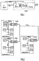
- FIG. 1 A known interface circuit, in a context of this type, is represented by FIG. 1. It comprises a PCC1008T circuit (described in the specification "Stand-Alone VAN-Controller PCC1008T", published by the company Philips-Semiconductors) which is intended to provide the interface between a microprocessor ( ⁇ P BAM) and an automotive type bus of VAN type (the acronym VAN corresponding to "Vehicle Area Network” which means "network within the framework of a vehicle”).
- ⁇ P BAM microprocessor
- VAN vehicle Area Network
- the PCC1008T circuit is connected to the VAN bus by a transmission circuit (TRANS) and, by means of a parallel connection, to a parallel port of the microprocessor in question ( ⁇ P BAM), which is intended for use as interface, and is in turn connected to the microcontroller ( ⁇ P applic) of an application by an I 2 C bus.
- the PCC1008T appears to the microprocessor as a peripheral organ organized like a memory, with four registers as an interface directly accessible for reading and four registers directly accessible for writing. It also has two VAN frame reception registers, used in turn. The structure of this interface circuit is relatively complex.
- An object of the invention is to provide an interface circuit which ensures a high degree of intelligence in communications between the bus specific to the automobile and the internal microcontroller (s) of a application, and directly ensures the connection between the external bus and the internal serial bus of the application, itself connected to the microcontroller of the application.
- the system according to the invention is remarkable in that it is furthermore provided with means for sending after complete reception of a message an I 2 C frame signifying that it has acquired all the data, and the circuit d the slave interface is further provided with means for, when it is a transmitter, to interpret the reception of such an I 2 C frame.
- the invention is notably based on the idea of combining in the same interface circuit an EEPROM type protocol with requirements for communication circuits.
- the interface circuit is advantageously provided with means for defining in its RAM for reception of the zones to be used by means of two address pointers updated at all times based on the carrying out of the tasks which are assigned to this reception memory, pointers that delimit, considering memory as circular, the areas available for reading and writing respectively. This allows the interface circuit to work with less memory memory, a memory of this type being expensive on the silicon surface.
- the interface circuit advantageously includes means for, if the request has been made by the microcontroller, activate the request line each time no frame has been received from outside for a while predetermined possibly programmable.
- the system represented by FIG. 2 comprises several devices called “application 1", “application 2", “application 3”.
- application 1 Inside an application, there is a type I 2 C interconnection bus to interconnect the internal elements of the application, in particular one or more microcontrollers “ ⁇ C1", “ ⁇ C2” and various integrated circuits specialized "IC1", “IC2”, ... “ICn”.
- the applications 1, 2, 3 are interconnected with one another by means of a so-called "VAN” bus, distinct from the bus I 2 C above.
- BAM interface circuits for "Bus Adapter Module" placed between the VAN bus and the I 2 C bus.
- MRQ cronym corresponding to "Master Request” which means: request from the master
- the invention relates to the BAM interface circuit. This allows communication between, on the one hand the microcontroller (s) ⁇ C1, ⁇ C2 contained in an application and communicating by the I 2 C bus, and on the other hand the VAN bus.
- the VAN bus is a serial type differential bus which transmits blocks information called "frames". All the frames of a VAN bus have the same constitution, which is predefined by an ISO standard (ISO / TC 22 / WG 1). This bus has two conductors that carry respectively a digital signal and the complementary signal of this digital signal, which provides better resistance to noise.
- a VAN signal frame includes several successive fields, with at the beginning a characteristic code at the start of the frame, then a field identification specifying the destination address of the frame, a command field indicating in particular the communication mode (writing or reading, acknowledgment of receipt message requested or not, nature of message), a data field proper, a control field of redundancy used to detect an error in the frame and containing a word calculated from the content of the entire message, a code of end of data, a possible period provided for an accused of reception, and an end of frame code.
- a coding called "Manchester” is used; it's coding in which a usual bit is coded on two time units (one unit of time being that of a Manchester unencoded bit) with a transition between the first and second time units; this transition is from 0 to 1 or from 1 to 0 depending on the logical value of the bit.
- one bit in four is encoded in Manchester, thus providing periodically transitions that can be used as clock pulses.
- the I 2 C bus is also a standard bus, which is particularly suitable for interconnecting integrated circuits with one another. It comprises two bi-directional lines of serial type with eight-bit words, one line being devoted to data, and the other to a clock. Each entity connected to the bus is addressable by means of a unique address and simple master / slave relationships exist between them.
- the VAN and I 2 C buses are both two-state buses, a dominant state and a recessive state.
- the recessive state is that which the bus takes when it is left "in the air", while the dominant state is imposed by a module linked to the bus.
- They are also both multi-masters, providing a collision detection protocol to prevent data degradation if two masters start a data transfer together. Bit-by-bit arbitration on a specific field of a frame is provided for this purpose, according to which the one of the masters who first provides a recessive state and sees this state contradicted by a dominant state imposed by the other master loses priority.
- the interface circuit BAM consists of a transmission element TR and a management element IC.
- the transmission element TR transmits / receives VAN frames and in particular detects certain errors on the basis of the redundancy provided by the two complementary conductors.
- the management element IC is provided with means for understanding the I 2 C frames which reach it and for carrying out the actions possibly requested by them, for example translating them into VAN frames and having them transmitted by the element TR. It is also provided with means for transforming the VAN frames coming from the TR element and transmitting them to the I 2 C bus, and with means for reporting errors on the VAN bus to the application microcontroller.
- the means in question here are essentially implemented in the form of software.
- an I 2 C bus it is possible to connect elements which are either masters or slaves.
- the microcontroller is the master of the I 2 C bus which it synchronizes, starts and stops the transmission.
- the other elements are slaves.
- some masters can also be slaves in a configuration with several masters. This can be the case for example in a radio reception application, comprising two microcontrollers ⁇ C1 and ⁇ C2 which can both be masters, as in "application 1" in the figure.
- the BAM interface circuit is always a slave.
- the microcontroller is addressed to the BAM interface circuit in the same way as it would be addressed to a memory called EEPROM, compatible with I 2 C.
- EEPROM a memory
- PCF8581 sold by the company Philips-Semiconductors
- the same types of addressing and the same I 2 C frame format are used to read the information from the BAM interface circuit and to send information to the BAM interface circuit.
- the basic interaction mode of the BAM interface device partly recalls the specification of the integrated circuit PCC1008T, mentioned above.
- a reception memory is provided in the element IC of the BAM interface circuit. It is necessary to have in this has enough memory to receive messages from each device connected to the application, messages whose length depends on the sending application.
- the buffer for receiving VAN frames from other applications is managed dynamically, i.e. its size is variable depending on the length of the recorded messages, by opposition to the integrated circuit PCC1008T, mentioned above, in which management is static. It includes a so-called reading area where VAN frames are ready to be read by the master microcontroller, and a so-called writing area where new frames can be received from outside.
- the flow of trade determines the size of the portion of reading and that of the writing part: as soon as a new frame is deposited in the writing area, the part of this area that contains the said frame becomes a reading area, which therefore increases correspondingly, and the writing area decreases accordingly.
- two pointers AD1 and AD2 are provided, which delimit the zones available for reading and writing respectively, considering memory as circular (which implies in particular that the value of the maximum address plus one is equal to the value of the minimum address).
- the reading address is defined between AD1 inclusive and AD2 excluded, in the sense of increasing addresses.
- the ⁇ C microcontroller can then read from reliably in the memory of the slave interface circuit.
- the area of reading is defined by the slave element (the interface circuit) of so that the information in this area is relevant and that the first bytes read by the master element define at its intention the number of bytes to read. If nevertheless the master element try to continue reading the memory of the slave element beyond AD2, the slave element no longer increments its own address pointer, the data line is released (recessive state), and therefore the master reads the decimal value 255 each time.
- the information in the reading zone is not being read by the master element, the information of length of zone to be read and address AD2 are updated to indicate to the master reader that there is a new frame to read. If on the other hand a certain length of information has already been read by the master element, only the address AD2 is updated, to indicate the new border between the zones available respectively for reading and writing.
- a service can also represent a service internal to the interface circuit BAM, for example the state of the VAN line.
- a "transmission” service which has as argument an NPV frame, containing among others an identifier field. An application will receive a frame VAN if and only if the identifier of this frame is contained in the reception configuration of the application.
- the I 2 C frames have the general structure represented by FIGS. 3 and 4.
- FIG. 3 represents for example a data transfer message from the microcontroller to the BAM interface circuit.
- This message includes a message start code (St) according to the I 2 C standard (i.e., the data line has a transition down while the clock line is high), a destination address byte ( Write adr), which is the address of the BAM interface circuit, one bit for an acknowledgment (A) from the BAM interface circuit, one byte for the number of the requested service (Serv n °), again a bit for an acknowledgment (A), a first data byte (DATA1), a bit for an acknowledgment (A), a second data byte (DATA2), and so on , the message being terminated by an end code (Sp) according to the I 2 C standard (the data line has an upward transition while the clock line is high).
- Each of the data bytes (DATA1, DATA2, etc.) corresponds to a parameter of the requested service.
- FIG. 4 represents a message like the previous one, but followed by a message read in the BAM interface circuit by the microcontroller.
- This message includes a message start code (St) as in the message in FIG. 2, a byte of destination address, that is to say that of the microcontroller in which the BAM interface circuit wants to write (Write adr ), a bit for an acknowledgment (A) from the microcontroller, a byte of the number of the requested service (Serv n °), and again a bit for an acknowledgment (A).
- the "stop" code is replaced by a "restart” code.
- Such a "restart” procedure allows a change of direction of communication between the master and the slave: after writing to the slave, the master reads the slave using the "read address” which follows the "restart” condition.
- a “stop” condition followed by “start” could also be appropriate, however by leaving the line in the inactive state after the stop, we could possibly allow another master to take control of the I 2 C bus, but do not that another master could speak to the slave while it was left hanging after the writing.
- the "restart” code is followed by a new address, which also indicates that a read is now requested, a bit for an acknowledgment (A) from the microcontroller, a first byte of data (DATA1), a bit for an acknowledgment (A), and so on.
- Any byte for which an acknowledgment (A) has been issued is considered by the transmitter as acquired by the receiver, and the element IC of the interface circuit increments the address pointer in its memory. Any byte for which no acknowledgment has been issued is considered not acquired by the receiver. Then the address pointer is not incremented.
- the reading memory of the slave element can be updated.
- the address AD1 is moved to the position of the last byte read by the master element, plus one.
- AD2 AD1 .
- the microcontroller can also ask for the service number again.
- One service among others is the service by which the I 2 C bus transfers general configuration data from the ⁇ C microcontroller to the BAM interface. Before transferring the configuration, the interface circuit must be reset to zero. Otherwise this service request is not admissible (no acknowledgment of receipt).
- the variables of the configuration the bits of the word which defines it
- there is a bit which will be called "StateSite” defining whether or not the MRQ line must be activated by the interface circuit each time that no frame n 'has been received from outside for a predetermined time, programmable or not. This procedure is different from that of observing VAN frames using a diagnostic logic circuit that does not differentiate between transmitted frames and received frames.
- the activation of the MRQ line triggers the reading of the state of the interface circuit by the master and the emission of a corresponding acknowledgment of receipt. As soon as the latter has been received, the MRQ line is released by the interface circuit and the "SiteSite" bit reset to zero in the status register.
- VAN bus a so-called VAN bus
- CAN bus developed by R. BOSCH GmbH and INTEL
- I-Bus type bus developed by the automobile manufacturer BMW
Landscapes
- Engineering & Computer Science (AREA)
- Theoretical Computer Science (AREA)
- Physics & Mathematics (AREA)
- General Engineering & Computer Science (AREA)
- General Physics & Mathematics (AREA)
- Mechanical Engineering (AREA)
- Small-Scale Networks (AREA)
- Information Transfer Systems (AREA)
Description
Claims (3)
- Système électronique de véhicule automobile comportant :une pluralité de dispositifs appelés applications comprenant chacun au moins un micro-contrôleur (µC1) et divers autres constituants (IC1-ICn), ainsi qu'un premier bus (I2C) de type I2C assurant les communications entre les constituants à l'intérieur de l'application,un second bus (VAN) de type série, différent du premier bus (I2C), assurant la communication des applications entre elles,et au niveau de chaque application un circuit d'interface (BAM) muni d'une mémoire vive de réception pour des messages et destiné à assurer une communication entre le premier bus (I2C) et le second bus (VAN), le micro-contrôleur (µC1) étant muni de moyens pour, lorsque, agissant en tant que maitre, il lit à partir du circuit d'interface esclave des données constituant un message, renvoyer un accusé de réception (A) après chaque octet reçu et pour, lorsqu'il ne désire plus lire, arrêter le message en ne renvoyant pas d'accusé de réception (A), caractérisé en ce que le micro-contrôleur (µC1) est en outre muni de moyens pour envoyer après réception complète d'un message une trame I2C (NA) signifiant qu'il a acquis toutes les données, et le circuit d'interface esclave (BAM) est en outre muni de moyens pour, lorsqu'il est émetteur, interpréter la réception d'une telle trame I2C.
- Système électronique pour véhicule automobile selon la revendication précédente, caractérisé en ce que le circuit d'interface (BAM) est muni de moyens pour définir dans sa mémoire de réception des zones à utiliser au moyen de deux pointeurs d'adresse mis à jour à chaque instant en fonction de la réalisation des tâches qui sont dévolues à cette mémoire de réception, pointeurs qui délimitent, en considérant la mémoire comme circulaire, les zones disponibles respectivement pour la lecture et l'écriture.
- Système électronique pour véhicule automobile selon l'une des revendications 1 ou 2, dans lequel est prévue une ligne dite de requête (MRQ) entre le circuit d'interface (BAM) et le micro-contrôleur (µC1), pour informer ce dernier lorsque de l'information nouvelle doit être acquise par lui, caractérisé en ce que le circuit d'interface (BAM) comporte des moyens pour, si la demande en a été faite par le micro-contrôleur (µC1), activer la ligne de requête à chaque fois qu'aucune trame n'a été reçue de l'extérieur depuis un temps prédéterminé éventuellement programmable.
Applications Claiming Priority (2)
| Application Number | Priority Date | Filing Date | Title |
|---|---|---|---|
| FR9401130 | 1994-02-02 | ||
| FR9401130 | 1994-02-02 |
Publications (2)
| Publication Number | Publication Date |
|---|---|
| EP0666199A1 EP0666199A1 (fr) | 1995-08-09 |
| EP0666199B1 true EP0666199B1 (fr) | 1999-09-29 |
Family
ID=9459665
Family Applications (1)
| Application Number | Title | Priority Date | Filing Date |
|---|---|---|---|
| EP95200197A Expired - Lifetime EP0666199B1 (fr) | 1994-02-02 | 1995-01-27 | Système électronique de véhicule automobile avec circuit d'interface entre deux bus différents |
Country Status (3)
| Country | Link |
|---|---|
| EP (1) | EP0666199B1 (fr) |
| JP (1) | JPH07253946A (fr) |
| DE (1) | DE69512443T2 (fr) |
Families Citing this family (7)
| Publication number | Priority date | Publication date | Assignee | Title |
|---|---|---|---|---|
| DE19600644C1 (de) * | 1996-01-10 | 1997-04-24 | Bosch Gmbh Robert | Schaltungsanordnung für in einem Kraftfahrzeug anordbare Funktionsmodule |
| DE19757335A1 (de) * | 1997-12-22 | 1999-07-01 | Siemens Ag | Schaltungsanordnung und Verfahren zum Übertragen von Daten über Datenleitungen |
| KR100291036B1 (ko) * | 1999-03-03 | 2001-05-15 | 윤종용 | 마이크로 콘트롤러와 표준 아이스퀘어씨 버스 프로토콜을 이용한시스템 하드웨어 관리 장치 및 방법 |
| DE10105858A1 (de) * | 2001-02-08 | 2002-08-14 | Deere & Co | Kommunikationssystem eines Fahrzeugs |
| JP3842144B2 (ja) * | 2002-02-20 | 2006-11-08 | 三菱電機株式会社 | 車載電子制御装置 |
| DE10212329B4 (de) * | 2002-03-20 | 2007-04-05 | Man Nutzfahrzeuge Ag | Elektroniksystem für ein Fahrzeug, insbesondere Nutzfahrzeug |
| FR2901211B1 (fr) * | 2006-05-17 | 2008-08-22 | Valeo Systemes Thermiques | Systeme d'adressage automatique d'actionneurs dans un vehicule automobile. |
Citations (1)
| Publication number | Priority date | Publication date | Assignee | Title |
|---|---|---|---|---|
| EP0451825A1 (fr) * | 1990-04-12 | 1991-10-16 | Sumitomo Wiring Systems, Ltd. | Système et méthode de multi-transmission pour un véhicule |
Family Cites Families (3)
| Publication number | Priority date | Publication date | Assignee | Title |
|---|---|---|---|---|
| DE3546683C3 (de) * | 1985-02-22 | 2003-10-09 | Bosch Gmbh Robert | Verfahren zum Betreiben einer Datenverarbeitungsanlage |
| DE4005087C1 (en) * | 1990-02-17 | 1991-08-01 | Gebr. Merten Gmbh & Co Kg, 5270 Gummersbach, De | Connector unit for domestic power installation - has adaptor for specific function allowing data transmission via bus and data lines |
| DE4392671C2 (de) * | 1992-06-10 | 2000-06-21 | Ford Werke Ag | Kommunikationssystem für Kraftfahrzeuge |
-
1995
- 1995-01-27 DE DE1995612443 patent/DE69512443T2/de not_active Expired - Fee Related
- 1995-01-27 EP EP95200197A patent/EP0666199B1/fr not_active Expired - Lifetime
- 1995-01-31 JP JP1402695A patent/JPH07253946A/ja active Pending
Patent Citations (1)
| Publication number | Priority date | Publication date | Assignee | Title |
|---|---|---|---|---|
| EP0451825A1 (fr) * | 1990-04-12 | 1991-10-16 | Sumitomo Wiring Systems, Ltd. | Système et méthode de multi-transmission pour un véhicule |
Non-Patent Citations (2)
| Title |
|---|
| Philips Semiconductors: "Stand-alone VAN-Controller PCC1008T"; Décembre 1992 * |
| Philips Semiconductors: "The I2C-bus and how to use it"; Janvier 1992 * |
Also Published As
| Publication number | Publication date |
|---|---|
| JPH07253946A (ja) | 1995-10-03 |
| DE69512443T2 (de) | 2000-05-04 |
| DE69512443D1 (de) | 1999-11-04 |
| EP0666199A1 (fr) | 1995-08-09 |
Similar Documents
| Publication | Publication Date | Title |
|---|---|---|
| BE1005695A3 (fr) | Procede de transmission commune de donnees audio et de donnees de commande numeriques sur un bus commun, systeme bus de mise en oeuvre du procede et interface pour une utilisation dans le procede. | |
| FR2896368A1 (fr) | Appareil pour ameliorer l'efficacite du microprogramme pour une interface serie multitrame | |
| EP0666199B1 (fr) | Système électronique de véhicule automobile avec circuit d'interface entre deux bus différents | |
| CA2006831C (fr) | Systeme d'emission de trames hdlc sur canal de type mic, a circuit hdlc unique et memoire tampon de transposition | |
| FR2988949A1 (fr) | Dispositif de communication et procede de programmation ou de correction d'erreur d'un ou plusieurs participants du dispositif de communication | |
| FR3009633A1 (fr) | Communication sur bus i2c | |
| EP3217290A1 (fr) | Systeme sur puce et procede d'echange de donnees entre noeuds de calculs d'un tel systeme sur puce | |
| EP0752669B1 (fr) | Dispositif de communication entre une pluralité de modules fonctionnels installés dans une unité locale et un bus externe de type ARINC 629 | |
| FR2676131A1 (fr) | Systeme de communication. | |
| FR2812437A1 (fr) | Procede et dispositif de communication entre un equipement exterieur a un vehicule automobile et des calculateurs embarques | |
| EP1304836B1 (fr) | Bus de terrain déterministe et procédé de gestion d'un tel bus | |
| FR2988934A1 (fr) | Dispositif de communication et procede de programmation ou de correction d'erreur d'un ou plusieurs participants du dispositif de communication | |
| FR2948785A1 (fr) | Terminateur de transaction | |
| FR2825812A1 (fr) | Procede de programmation/reprogrammation parallele de memoire flash embarquee par bus can | |
| FR2858076A1 (fr) | Procede et dispositif de synchronisation d'unites de trainement de donnees reliees par un reseau | |
| FR2680294A1 (fr) | Dispositif de transmission d'informations en differentiel entre au moins deux organes d'un vehicule automobile. | |
| FR3120267A1 (fr) | Communication sur bus I2C | |
| EP1011051A1 (fr) | Protocole et système de liaison par BUS entre éléments d'un microcontrôleur | |
| FR2642244A1 (fr) | Procede et dispositif d'acces hierarchise a un reseau de transmission d'informations | |
| FR2859853A1 (fr) | Procede de detection automatique du debit d'un reseau, notamment de type bus can, et de configuration au debit detecte, dispositif correspondant | |
| EP0484212B1 (fr) | Dispositif de reconnaissance d'adresses pour module électronique de traitement de données | |
| EP1426843B1 (fr) | Réseau local industriel ou domestique | |
| EP0709787A1 (fr) | Système de traitement d'informations comportant au moins deux processeurs | |
| FR2855925A1 (fr) | Procede de telecommunication entre un terminal local et un terminal central et systeme mettant en oeuvre le procede | |
| FR2538140A1 (fr) | Dispositif de couplage de bus pour systeme de traitement de donnees a bus multiples |
Legal Events
| Date | Code | Title | Description |
|---|---|---|---|
| PUAI | Public reference made under article 153(3) epc to a published international application that has entered the european phase |
Free format text: ORIGINAL CODE: 0009012 |
|
| AK | Designated contracting states |
Kind code of ref document: A1 Designated state(s): DE FR GB |
|
| 17P | Request for examination filed |
Effective date: 19960209 |
|
| 17Q | First examination report despatched |
Effective date: 19970205 |
|
| RAP1 | Party data changed (applicant data changed or rights of an application transferred) |
Owner name: PHILIPS ELECTRONICS N.V. Owner name: PHILIPS ELECTRONIQUE GRAND PUBLIC |
|
| RAP3 | Party data changed (applicant data changed or rights of an application transferred) |
Owner name: KONINKLIJKE PHILIPS ELECTRONICS N.V. Owner name: PHILIPS ELECTRONIQUE GRAND PUBLIC |
|
| GRAG | Despatch of communication of intention to grant |
Free format text: ORIGINAL CODE: EPIDOS AGRA |
|
| RAP1 | Party data changed (applicant data changed or rights of an application transferred) |
Owner name: MANNESMANN VDO AKTIENGESELLSCHAFT |
|
| GRAG | Despatch of communication of intention to grant |
Free format text: ORIGINAL CODE: EPIDOS AGRA |
|
| GRAH | Despatch of communication of intention to grant a patent |
Free format text: ORIGINAL CODE: EPIDOS IGRA |
|
| GRAH | Despatch of communication of intention to grant a patent |
Free format text: ORIGINAL CODE: EPIDOS IGRA |
|
| GRAA | (expected) grant |
Free format text: ORIGINAL CODE: 0009210 |
|
| AK | Designated contracting states |
Kind code of ref document: B1 Designated state(s): DE FR GB |
|
| REF | Corresponds to: |
Ref document number: 69512443 Country of ref document: DE Date of ref document: 19991104 |
|
| GBT | Gb: translation of ep patent filed (gb section 77(6)(a)/1977) |
Effective date: 19991116 |
|
| PLBQ | Unpublished change to opponent data |
Free format text: ORIGINAL CODE: EPIDOS OPPO |
|
| PLBI | Opposition filed |
Free format text: ORIGINAL CODE: 0009260 |
|
| PLBF | Reply of patent proprietor to notice(s) of opposition |
Free format text: ORIGINAL CODE: EPIDOS OBSO |
|
| 26 | Opposition filed |
Opponent name: BROSE FAHRZEUGTEILE GMBH & CO. KG Effective date: 20000629 |
|
| PLBF | Reply of patent proprietor to notice(s) of opposition |
Free format text: ORIGINAL CODE: EPIDOS OBSO |
|
| PLBF | Reply of patent proprietor to notice(s) of opposition |
Free format text: ORIGINAL CODE: EPIDOS OBSO |
|
| REG | Reference to a national code |
Ref country code: GB Ref legal event code: IF02 |
|
| RTI2 | Title (correction) |
Free format text: ELECTRONIC SYSTEM OF AN AUTOMOBILE WITH AN INTERFACE CIRCUIT BETWEEN TWO DIFFERENT BUSSES |
|
| PLBO | Opposition rejected |
Free format text: ORIGINAL CODE: EPIDOS REJO |
|
| RTI2 | Title (correction) |
Free format text: ELECTRONIC SYSTEM OF AN AUTOMOBILE WITH AN INTERFACE CIRCUIT BETWEEN TWO DIFFERENT BUSSES |
|
| RTI2 | Title (correction) |
Free format text: ELECTRONIC SYSTEM OF AN AUTOMOBILE WITH AN INTERFACE CIRCUIT BETWEEN TWO DIFFERENT BUSSES |
|
| PLBN | Opposition rejected |
Free format text: ORIGINAL CODE: 0009273 |
|
| STAA | Information on the status of an ep patent application or granted ep patent |
Free format text: STATUS: OPPOSITION REJECTED |
|
| 27O | Opposition rejected |
Effective date: 20020525 |
|
| PGFP | Annual fee paid to national office [announced via postgrant information from national office to epo] |
Ref country code: GB Payment date: 20030114 Year of fee payment: 9 |
|
| PGFP | Annual fee paid to national office [announced via postgrant information from national office to epo] |
Ref country code: DE Payment date: 20030317 Year of fee payment: 9 |
|
| PG25 | Lapsed in a contracting state [announced via postgrant information from national office to epo] |
Ref country code: GB Free format text: LAPSE BECAUSE OF NON-PAYMENT OF DUE FEES Effective date: 20040127 |
|
| PG25 | Lapsed in a contracting state [announced via postgrant information from national office to epo] |
Ref country code: DE Free format text: LAPSE BECAUSE OF NON-PAYMENT OF DUE FEES Effective date: 20040803 |
|
| GBPC | Gb: european patent ceased through non-payment of renewal fee |
Effective date: 20040127 |
|
| PGFP | Annual fee paid to national office [announced via postgrant information from national office to epo] |
Ref country code: FR Payment date: 20050127 Year of fee payment: 11 |
|
| PG25 | Lapsed in a contracting state [announced via postgrant information from national office to epo] |
Ref country code: FR Free format text: LAPSE BECAUSE OF NON-PAYMENT OF DUE FEES Effective date: 20060131 |
|
| REG | Reference to a national code |
Ref country code: FR Ref legal event code: ST Effective date: 20060929 |