EP0669789A1 - Circuit pour alimenter au moins une lampe à décharge basse-pression - Google Patents
Circuit pour alimenter au moins une lampe à décharge basse-pression Download PDFInfo
- Publication number
- EP0669789A1 EP0669789A1 EP95101851A EP95101851A EP0669789A1 EP 0669789 A1 EP0669789 A1 EP 0669789A1 EP 95101851 A EP95101851 A EP 95101851A EP 95101851 A EP95101851 A EP 95101851A EP 0669789 A1 EP0669789 A1 EP 0669789A1
- Authority
- EP
- European Patent Office
- Prior art keywords
- circuit arrangement
- inverter
- voltage
- lamp
- control unit
- Prior art date
- Legal status (The legal status is an assumption and is not a legal conclusion. Google has not performed a legal analysis and makes no representation as to the accuracy of the status listed.)
- Granted
Links
- 239000003990 capacitor Substances 0.000 claims abstract description 32
- 230000008878 coupling Effects 0.000 claims description 3
- 238000010168 coupling process Methods 0.000 claims description 3
- 238000005859 coupling reaction Methods 0.000 claims description 3
- 230000001105 regulatory effect Effects 0.000 claims description 3
- 230000005669 field effect Effects 0.000 description 5
- 230000007704 transition Effects 0.000 description 4
- 230000001419 dependent effect Effects 0.000 description 2
- 238000009499 grossing Methods 0.000 description 2
- 238000010438 heat treatment Methods 0.000 description 2
- 238000011144 upstream manufacturing Methods 0.000 description 2
- 230000001276 controlling effect Effects 0.000 description 1
- 238000000034 method Methods 0.000 description 1
Images


Classifications
-
- H—ELECTRICITY
- H05—ELECTRIC TECHNIQUES NOT OTHERWISE PROVIDED FOR
- H05B—ELECTRIC HEATING; ELECTRIC LIGHT SOURCES NOT OTHERWISE PROVIDED FOR; CIRCUIT ARRANGEMENTS FOR ELECTRIC LIGHT SOURCES, IN GENERAL
- H05B41/00—Circuit arrangements or apparatus for igniting or operating discharge lamps
- H05B41/14—Circuit arrangements
- H05B41/36—Controlling
- H05B41/38—Controlling the intensity of light
- H05B41/39—Controlling the intensity of light continuously
- H05B41/392—Controlling the intensity of light continuously using semiconductor devices, e.g. thyristor
- H05B41/3921—Controlling the intensity of light continuously using semiconductor devices, e.g. thyristor with possibility of light intensity variations
- H05B41/3927—Controlling the intensity of light continuously using semiconductor devices, e.g. thyristor with possibility of light intensity variations by pulse width modulation
-
- H—ELECTRICITY
- H05—ELECTRIC TECHNIQUES NOT OTHERWISE PROVIDED FOR
- H05B—ELECTRIC HEATING; ELECTRIC LIGHT SOURCES NOT OTHERWISE PROVIDED FOR; CIRCUIT ARRANGEMENTS FOR ELECTRIC LIGHT SOURCES, IN GENERAL
- H05B41/00—Circuit arrangements or apparatus for igniting or operating discharge lamps
- H05B41/14—Circuit arrangements
- H05B41/26—Circuit arrangements in which the lamp is fed by power derived from DC by means of a converter, e.g. by high-voltage DC
- H05B41/28—Circuit arrangements in which the lamp is fed by power derived from DC by means of a converter, e.g. by high-voltage DC using static converters
- H05B41/295—Circuit arrangements in which the lamp is fed by power derived from DC by means of a converter, e.g. by high-voltage DC using static converters with semiconductor devices and specially adapted for lamps with preheating electrodes, e.g. for fluorescent lamps
-
- Y—GENERAL TAGGING OF NEW TECHNOLOGICAL DEVELOPMENTS; GENERAL TAGGING OF CROSS-SECTIONAL TECHNOLOGIES SPANNING OVER SEVERAL SECTIONS OF THE IPC; TECHNICAL SUBJECTS COVERED BY FORMER USPC CROSS-REFERENCE ART COLLECTIONS [XRACs] AND DIGESTS
- Y10—TECHNICAL SUBJECTS COVERED BY FORMER USPC
- Y10S—TECHNICAL SUBJECTS COVERED BY FORMER USPC CROSS-REFERENCE ART COLLECTIONS [XRACs] AND DIGESTS
- Y10S315/00—Electric lamp and discharge devices: systems
- Y10S315/04—Dimming circuit for fluorescent lamps
Definitions
- the invention relates to a circuit arrangement for operating at least one low-pressure discharge lamp according to the preamble of patent claim 1.
- a circuit arrangement corresponding to the preamble of claim 1 is described, for example, in patent specification EP 0 059 064.
- This circuit arrangement has an externally controlled inverter which feeds a low-pressure discharge lamp with preheated electrode filaments via a series resonant circuit.
- the lamp is supplied with a current by the inverter, the frequency of which is far above the resonance frequency of the series resonance circuit.
- the switching frequency of the inverter is shifted in the direction of the resonance frequency of the series resonance circuit in order to generate the required ignition voltage by means of resonance increase.
- the lamp is then operated at a frequency which is slightly above the resonance frequency of the series resonance circuit now damped by the lamp.
- the switching frequency of the inverter and thus the frequency of the lamp current is increased again as a function of the setting on the dimming device.
- the reduced impedance of the resonance capacitance connected in parallel with the discharge lamp due to the frequency increase causes a reduction in the lamp current. In this way, a change in the inverter switching frequency brings about a brightness control of the low-pressure discharge lamp.
- German patent 33 38 464 discloses a circuit arrangement with a self-oscillating inverter for operating a dimmable fluorescent lamp, in which the brightness control of the fluorescent lamp takes place via a change in the duty cycle of the high-frequency AC voltage generated by the inverter as a function of the setting on the dimming device.
- circuits of the documents cited above require a comparatively high amount of circuitry and also have the disadvantage that the fluorescent lamps burn immediately at full power immediately after ignition, regardless of the setting on the dimming device, before the control unit matches the frequency or the duty cycle of the inverter has adjusted the setting on the dimmer.
- the circuit arrangement disclosed here also has a half-bridge inverter which feeds a fluorescent lamp via a series resonant circuit.
- the brightness control of the lamp takes place in the manner of a phase control.
- a bridging switch arranged parallel to the lamp bridges the fluorescent lamp during a controllable phase angle of the lamp current which is dependent on the setting on the dimming device.
- the current flowing over the discharge path is thereby weakened in accordance with the setting on the dimming device.
- the adjustment of the bypass switch to the switching phases of the inverter requires a lot of circuitry.
- the circuit arrangement according to the invention essentially consists of an inverter with a downstream LC output circuit for the voltage supply of the low-pressure discharge lamp or low-pressure discharge lamps, a DC voltage supply unit for the inverter, a control unit and a dimming device with which the brightness of the lamp or lamps is adjusted.
- the dimming device and the control unit are connected to the DC voltage supply unit in such a way that the control unit sets the supply voltage for the inverter to a value which depends on the selected setting on the dimming device.
- the inverter supply voltage which is reduced in accordance with the setting on the dimming device, brings about a reduced lamp current at a constant or approximately constant operating frequency of the inverter, so that the low-pressure discharge lamp burns with reduced power.
- the particularly preferred embodiments are a circuit arrangement for operating a fluorescent lamp, in particular for dimming a fluorescent lamp.
- the fluorescent lamp is supported by a half bridge inverter with a series resonance circuit, in which the lamp is integrated.
- the DC voltage supply for the half-bridge inverter is provided by a DC voltage supply unit, preferably designed as an inverse or flyback converter, the DC voltage output of which is connected to the input of the inverter.
- the switching transistor of the inverse or flyback converter receives a control signal from the control unit, which forms the control unit from the setpoint specified by the dimming device and the inverter supply voltage applied to the output capacitor of the DC voltage supply unit as a control variable.
- the output voltage of the DC voltage supply unit is set by the control unit and the dimming device during lamp operation.
- the electrode filaments of the fluorescent lamp are usually preheated.
- the duration of the electrode preheating and the level of the heating voltage must be independent of the preset lamp brightness. Therefore, the control signal of the dimming device has no influence on the control unit during the electrode preheating phase.
- the transition from the electrode preheating phase to the dimming operation is advantageously carried out by means of a timer which triggers a relay at the end of the preheating phase, which bridges the electrode filaments for igniting the lamp for a short time, and which at the same time ensures that the control unit adjusts the setting on the dimming device Takes over the value for the lamp brightness. This ensures that the lamp burns immediately after starting with the brightness set by the dimmer.
- the resonance capacitance arranged parallel to the discharge gap consists of two capacitors connected in parallel with one another. During the preheating phase and also during lamp operation (after the lamp has been ignited), both resonance capacitors are integrated in the series resonance circuit. During the ignition phase, however, one of the two capacitors is switched out of the series resonance circuit by the relay.
- the highly schematic Figure 1 illustrates the basic principle of the circuit arrangement according to the invention. It has a self-oscillating half-bridge inverter T1, T2 with a series resonance circuit connected downstream for the voltage supply of a fluorescent lamp L.
- the series resonance circuit contains a coupling capacitor CK, a resonance inductance LD, a resonance capacitance CR and the electrode filaments E1, E2 of the lamp L. All these components are connected in series, wherein the resonance capacitance CR is integrated between the two electrode filaments E1, E2 in the series resonant circuit in such a way that it is arranged parallel to the discharge path of the lamp L.
- the half-bridge inverter T1, T2 receives its supply voltage from the output capacitor C1 of a DC voltage supply unit.
- a control unit ST controls the half-bridge transistors T1, T2.
- the working frequency of this half-bridge inverter is close to the resonance frequency of the components CR, LR of its output circuit.
- a dimming device D is connected to the output C1 of the DC voltage supply unit via a control unit R.
- the supply voltage for the inverter T1, T2 provided at the output capacitor C1 is dependent on the control unit R. speed regulated by the setting on the dimmer.
- a lower supply voltage for the half-bridge T1, T2 causes a lower current through the lamp L, which therefore burns with reduced power.
- FIG. 2 shows the DC voltage supply unit for the half-bridge inverter T1, T2 operated with mains voltage according to a first exemplary embodiment. It consists of an inverse converter with an upstream rectifier G and a high-frequency filter F, which prevents high-frequency interference signals from being coupled into the power grid. A description of a commonly used high-frequency filter F can be found, for example, in European Patent Application EP 0 541 909. A smoothing capacitor C is connected in parallel with the DC voltage output of the rectifier G in order to smooth the rectified mains voltage.
- the inverse converter consists of a field effect transistor T, an inductor L, a diode D and an electrolytic capacitor C1 which is connected in parallel to the output of the inverse converter.
- a first input of the control unit R is connected in parallel to the output capacitor C1 of the inverse converter, while a second input of the control unit R is connected to the output of the dimmer D.
- the output of the control unit R is led to the gate connection of the field effect transistor T.
- the reference symbols V1, V2 and V3 define interfaces at which the circuit arrangement according to the invention has been separated for the sake of clarity.
- the circuits of FIGS. 2 and 4 must be put together again at these interfaces.
- the half-bridge inverter T1, T2 thus receives its supply voltage from the capacitor C1 via the interfaces V1, V2 and the timer ZS is connected to a third input of the control unit R via the interface V3.
- the inverter is designed as a self-oscillating, current-feedback half-bridge inverter T1, T2.
- a series resonance circuit is connected to the center tap of the half bridge T1, T2, which comprises a coupling capacitor CK, a resonance inductor LD, a resonance capacitance CR and the electrode filaments E1, E2 of the fluorescent lamp L. All of the components of the series resonant circuit mentioned are connected in series. However, the resonance capacitance CR is integrated in the series resonance circuit in such a way that it is connected in parallel to the discharge path of the lamp L.
- the circuit arrangement has two switching contacts K1, K2, which are each connected in parallel to one of the electrode filaments E1, E2 and are controlled by the relay RE.
- the relay RE is also connected to the time switch ZS.
- the inverse converter at the electrolytic capacitor C1 builds up the supply voltage for the half-bridge inverter T1, T2.
- This supply voltage is initially independent of the setting on the dimming device and its value is selected so that during the electrode preheating phase the voltage generated by the half bridge T1, T2 at the center tap ensures a sufficient current for electrode preheating through the series resonant circuit.
- the relay contacts K1, K2 are open, so that the electrode coils E1, E2 are serially integrated in the series resonance circuit and a high-frequency heating current flows through them.
- the resistance of the electrode coils E1, E2 dampens the series resonance circuit and prevents the lamp L from igniting.
- the time switch ZS triggers the relay RE, so that both relay contacts K1, K2 are briefly closed for a period of approximately 8 ms are, and simultaneously activates the control unit R.
- the electrode coils E1, E2 are bridged and the series resonance circuit is damped.
- the ignition voltage for the fluorescent lamp L builds up at the resonance capacitance CR.
- the relay contacts K1, K2 are open again during normal lamp operation, that is to say after the lamp L has been ignited.
- the control unit R activated by the time switch ZS detects the supply voltage applied to the output capacitor C1 for the inverter ter T1, T2 and compares this with the setpoint determined by the setting on the dimming device and supplied by the dimming device R and controls the pulse duty factor of this transistor T via its connection to the gate electrode of the field effect transistor T and thus regulates the output voltage of the inverse converter at the electrolytic capacitor C1 .
- a reduced output voltage of the inverse converter means a reduced supply voltage for the half-bridge inverter T1, T2.
- the voltage drop at the center tap of the half-bridge inverter T1, T2 is then also reduced accordingly, so that a reduced current flows through the series resonance circuit and over the discharge path of the lamp L. In this way, the power and the brightness of the fluorescent lamp L are controlled by regulating the inverter supply voltage as a function of the setting on the dimming device.
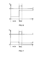
- FIGS. 6 and 7 illustrate the timing of the control signals for the relay RE (curve 1 in each case) and for the control unit R (curve 2 in each case) during the transition from the electrode preheating phase to normal lamp operation for two different dimmer settings.
- the control signal for the control unit R (FIGS. 6 and 7, curve 2) and thus also the control voltage for the gate electrode of the transistor T is independent of the setting on the dimming device D.
- the relay RE receives no control signal and the switch contacts K1, K2 are open. Only at the beginning of the ignition phase is the control unit R activated and the gate electrode of the transistor T receives different control signals in accordance with the dimmer settings.
- the ignition phase lasts approx. 8 ms.
- the relay RE receives a control signal that closes both relay contacts K1, K2. After the lamp L has been ignited, both relay contacts are open again, the relay RE receives no control signal and the control voltage for the gate electrode of the transistor T is determined by the setting on the dimming device D and by the control unit R.
- FIG. 5 shows a second embodiment of the circuit arrangement according to the invention. At the interfaces V1, V2 and V3, it is connected to the inverse converter shown in FIG. It differs from the first embodiment only in the resonance capacitance.
- the resonance capacitance is designed in two parts in the second embodiment. It consists of the resonance capacitors CR1 and CR2 connected in parallel, both of which are arranged parallel to the discharge path of the lamp. During the preheating phase and after the lamp has started, both resonance capacitors CR1, CR2 are integrated in the series resonance circuit (position of the switching contacts K1, K2 as shown in FIG. 5).
- the resonance capacitor CR2 is switched out of the series resonance circuit by briefly switching the relay contacts K1, K2, so that only the capacitance of the capacitor CR1 is effective.
- This measure allows the voltage drop across the discharge path of the lamp L to be reduced during the preheating phase and increased during the ignition phase. In this way, cold starts of the fluorescent lamp L are avoided, on the one hand, and a safe lamp start during the ignition phase, on the other hand, is made possible.
- the flyback converter shown in FIG. 3 can also be used to supply power to the half-bridge inverter T1, T2.
- the flyback converter is fed via the high-frequency filter F and the rectifier G with the rectified mains voltage smoothed by the smoothing capacitor C '. It consists of a field effect transistor T ', a transformer TR, a diode D' and the electrolytic capacitor C1 connected in parallel with its output.
- a description of the structure and operation of a flyback converter can be found, for example, in the book "Clocked Power Supply" by J. Beckmann, Franzis-Verlag GmbH, pages 19-24 and is therefore not to be explained in more detail here.
- the control unit R and the dimming device D are, as already described in the first exemplary embodiment, connected to the gate electrode of the field effect transistor T 'and the output capacitor C1 of the flyback converter.
- the control unit R uses the pulse duty factor of the transistor T 'to control the supply voltage applied to the electrolytic capacitor C1 for the half-bridge inverter T1, T2 as a function of the selected setting on the dimming device.
- the regulation of the inverter voltage supply according to the setting on the dimming device is also activated in this exemplary embodiment only at the beginning of the ignition phase by the time switch ZS.
- the reference symbols V1, V2 and V3 define interfaces via which the flyback converter shown in FIG. 3 is connected to one of the circuits shown in FIG. 4 or 5 according to the first or second exemplary embodiment.
- the dimming device D, the time switch ZS and the control unit R can be implemented in different ways.
- the dimming device D generates a voltage between approx. 1 V (lowest dimming level) and 10 V (highest dimming level) at the input of the control unit R. In the simplest case, this can be achieved, for example, using a dimming potentiometer.
- a time switch ZS For example, an RC element with a downstream comparator is suitable. The time constant of this RC element essentially determines the duration of the electrode preheating phase.
- the control unit R can be implemented, for example, as a PI or PID controller with an upstream subtractor.
- the subtractor forms a differential voltage from the dimmer signal and, for example, from a voltage signal proportional to the supply voltage of the inverter, from which a signal for controlling the gate electrode of the transistor T, T 'of the DC voltage supply unit is derived.
- the power of the lamp L can be dimmed down to 5% of its nominal value.
Landscapes
- Circuit Arrangements For Discharge Lamps (AREA)
- Discharge-Lamp Control Circuits And Pulse- Feed Circuits (AREA)
- Inverter Devices (AREA)
Applications Claiming Priority (2)
| Application Number | Priority Date | Filing Date | Title |
|---|---|---|---|
| DE4406083 | 1994-02-24 | ||
| DE4406083A DE4406083A1 (de) | 1994-02-24 | 1994-02-24 | Schaltungsanordnung zum Betrieb mindestens einer Niederdruckentladungslampe |
Publications (2)
| Publication Number | Publication Date |
|---|---|
| EP0669789A1 true EP0669789A1 (fr) | 1995-08-30 |
| EP0669789B1 EP0669789B1 (fr) | 1999-09-29 |
Family
ID=6511155
Family Applications (1)
| Application Number | Title | Priority Date | Filing Date |
|---|---|---|---|
| EP95101851A Expired - Lifetime EP0669789B1 (fr) | 1994-02-24 | 1995-02-10 | Circuit pour alimenter au moins une lampe à décharge basse-pression |
Country Status (4)
| Country | Link |
|---|---|
| US (1) | US5493182A (fr) |
| EP (1) | EP0669789B1 (fr) |
| JP (1) | JP3771291B2 (fr) |
| DE (2) | DE4406083A1 (fr) |
Cited By (1)
| Publication number | Priority date | Publication date | Assignee | Title |
|---|---|---|---|---|
| EP0771440A4 (fr) * | 1994-06-28 | 1997-07-30 | Energy Savings Inc | Protection electronique pouvant etre attenuee par un gradateur exterieur |
Families Citing this family (25)
| Publication number | Priority date | Publication date | Assignee | Title |
|---|---|---|---|---|
| EP0926928B1 (fr) * | 1997-04-17 | 2005-01-05 | Toshiba Lighting & Technology Corporation | Piece d'eclairage a lampe a decharge et dispositif de commande d'eclairage |
| US5949197A (en) * | 1997-06-30 | 1999-09-07 | Everbrite, Inc. | Apparatus and method for dimming a gas discharge lamp |
| DK1042942T3 (da) * | 1997-07-24 | 2002-12-02 | Noontek Ltd | Elektronisk ballast til en gasudladningslampe |
| JP2982804B2 (ja) * | 1998-01-16 | 1999-11-29 | サンケン電気株式会社 | 放電灯点灯装置 |
| ES2226346T3 (es) * | 1998-02-13 | 2005-03-16 | Lutron Electronics Co., Inc. | Balasto atenuador electronico. |
| US6259215B1 (en) | 1998-08-20 | 2001-07-10 | Romlight International, Inc. | Electronic high intensity discharge ballast |
| US7592753B2 (en) * | 1999-06-21 | 2009-09-22 | Access Business Group International Llc | Inductively-powered gas discharge lamp circuit |
| DE19941437A1 (de) * | 1999-08-30 | 2001-03-01 | Patent Treuhand Ges Fuer Elektrische Gluehlampen Mbh | Schaltungsanordnung zum Betrieb mindestens einer Entladungslampe |
| CN1304277A (zh) | 1999-10-25 | 2001-07-18 | 俞志龙 | 一种适合调光用荧光灯电子镇流器 |
| JP2002015892A (ja) * | 2000-06-28 | 2002-01-18 | Matsushita Electric Ind Co Ltd | 放電ランプ点灯装置 |
| TW530521B (en) * | 2000-08-28 | 2003-05-01 | Koninkl Philips Electronics Nv | Circuit device for operating a high-pressure discharge lamp with successive current phases |
| US6396220B1 (en) * | 2001-05-07 | 2002-05-28 | Koninklijke Philips Electronics N.V. | Lamp ignition with compensation for parasitic loading capacitance |
| US6498441B1 (en) * | 2001-08-10 | 2002-12-24 | Koninklijke Philips Electronics N.V. | Method for coloring mixing of hid lamps operated at VHF frequencies using duty cycle modulation |
| US6963176B2 (en) * | 2001-12-25 | 2005-11-08 | Matsushita Electric Works, Ltd. | Discharge lamp operation apparatus |
| DE10204432A1 (de) * | 2002-02-04 | 2003-09-11 | Tridonicatco Gmbh & Co Kg | Elektronisches Vorschaltgerät mit Wendelheizung |
| US6934168B2 (en) * | 2003-02-27 | 2005-08-23 | International Rectifier Corporation | Single stage PFC and power converter unit |
| TWM265641U (en) * | 2004-06-09 | 2005-05-21 | Rilite Corportation | Double shielded electroluminescent panel |
| DE102004050110A1 (de) * | 2004-10-14 | 2006-04-27 | Fab Consulting Gmbh | Verfahren und Schaltungsanordnung zum Betreiben von Entladungslampen an ein- oder mehrphasigen Netzen mittels Vorschaltgerät |
| US7336041B2 (en) * | 2004-12-06 | 2008-02-26 | Vicente Aldape Ayala | Automatic light dimmer for electronic and magnetic ballasts (fluorescent or HID) |
| DE102005022592A1 (de) * | 2005-05-17 | 2006-11-23 | Patent-Treuhand-Gesellschaft für elektrische Glühlampen mbH | Schaltungsanordnung zum Betrieb einer Entladungslampe mit schaltbarem Resonanzkondensator |
| JP2007026788A (ja) * | 2005-07-14 | 2007-02-01 | Osram-Melco Ltd | 無電極放電ランプ照明装置 |
| US7372216B2 (en) * | 2006-04-03 | 2008-05-13 | Ceelite Llc | Constant brightness control for electro-luminescent lamp |
| US7821208B2 (en) * | 2007-01-08 | 2010-10-26 | Access Business Group International Llc | Inductively-powered gas discharge lamp circuit |
| US7911153B2 (en) * | 2007-07-02 | 2011-03-22 | Empower Electronics, Inc. | Electronic ballasts for lighting systems |
| JP2011082077A (ja) * | 2009-10-09 | 2011-04-21 | Hitachi Appliances Inc | 点灯装置及びそれを用いた液晶表示装置 |
Citations (2)
| Publication number | Priority date | Publication date | Assignee | Title |
|---|---|---|---|---|
| GB2212995A (en) * | 1987-10-23 | 1989-08-02 | Rockwell International Corp | Fluorescent lamp dimmer |
| WO1993007732A1 (fr) * | 1991-10-03 | 1993-04-15 | Motorola Lighting Inc. | Circuit de commande d'une charge de lampe a decharge |
Family Cites Families (11)
| Publication number | Priority date | Publication date | Assignee | Title |
|---|---|---|---|---|
| EP0059064B1 (fr) * | 1981-02-21 | 1985-10-02 | THORN EMI plc | Circuit de démarrage et d'exploitation de lampes |
| DE3338464C2 (de) * | 1983-10-22 | 1987-03-05 | Plankenhorn Kapitalverwaltungs-KG, 7208 Spaichingen | Schaltungsanordnung zum Betrieb mindestens einer Leuchtstofflampe mit einstellbarer Helligkeit an einem selbstschwingenden Wechselrichter |
| DE3623749A1 (de) * | 1986-07-14 | 1988-01-21 | Patent Treuhand Ges Fuer Elektrische Gluehlampen Mbh | Schaltungsanordnung zum betrieb von niederdruckentladungslampen |
| US5187414A (en) * | 1988-07-15 | 1993-02-16 | North American Philips Corporation | Fluorescent lamp controllers |
| US5041763A (en) * | 1989-12-22 | 1991-08-20 | Lutron Electronics Co., Inc. | Circuit and method for improved dimming of gas discharge lamps |
| DE8915386U1 (de) * | 1989-12-29 | 1991-04-25 | Zumtobel Ag, Dornbirn | Vorschaltgerät zum Dimmen von Leuchtstoffröhren |
| DE4005850A1 (de) * | 1990-02-23 | 1991-08-29 | Patent Treuhand Ges Fuer Elektrische Gluehlampen Mbh | Schaltungsanordnung zum betrieb einer entladungslampe |
| DE9100552U1 (de) * | 1990-04-28 | 1991-04-11 | Trilux-Lenze Gmbh + Co Kg, 5760 Arnsberg | Leuchtstofflampen-Vorschaltgerät |
| US5262701A (en) * | 1991-03-15 | 1993-11-16 | U.S. Philips Corporation | Circuit arrangement for operating a high pressure sodium lamp |
| DE4137207A1 (de) * | 1991-11-12 | 1993-05-13 | Patent Treuhand Ges Fuer Elektrische Gluehlampen Mbh | Schaltungsanordnung zum betrieb von entladungslampen |
| US5394064A (en) * | 1993-10-15 | 1995-02-28 | Micro-Technology Inc.-Wisconsin | Electronic ballast circuit for fluorescent lamps |
-
1994
- 1994-02-24 DE DE4406083A patent/DE4406083A1/de not_active Withdrawn
- 1994-12-21 JP JP33566694A patent/JP3771291B2/ja not_active Expired - Fee Related
-
1995
- 1995-01-17 US US08/373,396 patent/US5493182A/en not_active Expired - Lifetime
- 1995-02-10 EP EP95101851A patent/EP0669789B1/fr not_active Expired - Lifetime
- 1995-02-10 DE DE59506923T patent/DE59506923D1/de not_active Expired - Fee Related
Patent Citations (2)
| Publication number | Priority date | Publication date | Assignee | Title |
|---|---|---|---|---|
| GB2212995A (en) * | 1987-10-23 | 1989-08-02 | Rockwell International Corp | Fluorescent lamp dimmer |
| WO1993007732A1 (fr) * | 1991-10-03 | 1993-04-15 | Motorola Lighting Inc. | Circuit de commande d'une charge de lampe a decharge |
Non-Patent Citations (1)
| Title |
|---|
| "COMBINED DIMMER AND VOLTAGE REGULATOR CIRCUIT FOR FLUORESCENT LAMP INVERTER", IBM TECHNICAL DISCLOSURE BULLETIN, vol. 35, no. 7, 1 December 1992 (1992-12-01), pages 28 - 29, XP000332933 * |
Cited By (1)
| Publication number | Priority date | Publication date | Assignee | Title |
|---|---|---|---|---|
| EP0771440A4 (fr) * | 1994-06-28 | 1997-07-30 | Energy Savings Inc | Protection electronique pouvant etre attenuee par un gradateur exterieur |
Also Published As
| Publication number | Publication date |
|---|---|
| JP3771291B2 (ja) | 2006-04-26 |
| EP0669789B1 (fr) | 1999-09-29 |
| DE59506923D1 (de) | 1999-11-04 |
| JPH07245189A (ja) | 1995-09-19 |
| US5493182A (en) | 1996-02-20 |
| DE4406083A1 (de) | 1995-08-31 |
Similar Documents
| Publication | Publication Date | Title |
|---|---|---|
| EP0669789B1 (fr) | Circuit pour alimenter au moins une lampe à décharge basse-pression | |
| DE60122727T2 (de) | Intregrierte schaltung zur lampenerwärmung und dimmersteuerung | |
| EP0701389B1 (fr) | Circuit pour commander l'intensité lumineuse et le mode de functionnement de lampes à décharge | |
| DE69919138T2 (de) | Electronischer dimmer | |
| DE69614471T2 (de) | Vorschaltgerät für eine entladungslampe | |
| EP0748146B1 (fr) | Circuit pour le chauffage des électrodes de lampes à décharge | |
| DE69818941T2 (de) | Vorschaltgerät | |
| DE60225425T2 (de) | Elektronisch dimmbare ballastschaltung für eine hochintensitätsentladungslampe | |
| DE69916251T2 (de) | Elektron9sches hochfrequenzvorschaltgerät zum unabhängigen betrieb von mehreren lampen | |
| EP0801881B1 (fr) | Procede permettant de faire fonctionner au moins une lampe a fluorescence au moyen d'un ballast electronique et ballast electronique utilise a cet effet | |
| DE3101568C2 (de) | Schaltungsanordnung zum Betrieb von Niederdruckentladungslampen mit einstellbarem Lichtstrom | |
| EP0707438A2 (fr) | Ballast pour au moins une lampe à décharge | |
| DE19923945A1 (de) | Elektronisches Vorschaltgerät für mindestens eine Niederdruck-Entladungslampe | |
| EP1465330B1 (fr) | Procédé et circuit pour varier la consommation de puissance de charges capacitives | |
| DE60106336T2 (de) | Vorschaltgerät für Entladungslampe | |
| EP0435228B2 (fr) | Circuit pour alimenter (et amorcer) une lampe à décharge | |
| EP0439240B1 (fr) | Ballast électronique | |
| EP2266374B1 (fr) | Régulation de puissance de lampes à décharge dans des circuits en demi-pont ou en pont intégral | |
| DE3910738A1 (de) | Vorschaltgeraet fuer eine direkt geheizte entladungslampe | |
| DE102004044180A1 (de) | Elektronisches Vorschaltgerät mit Pumpschaltung für Entladungslampe mit vorheizbaren Elektroden | |
| EP1860925B1 (fr) | Appareil de montage de lampe électronique à connexion à chaud | |
| EP0165893B2 (fr) | Dispositif de commande de luminosité pour une lampe fluorescente | |
| DE102011000441B4 (de) | Betriebssteuergerät und Verfahren zum Dimmen eines Leuchtmittels über die Versorgungsspannung und die Spannungsfrequenz | |
| EP1189486B1 (fr) | Ballast électronique | |
| DE4010112A1 (de) | Schaltungsanordnung und verfahren zum betreiben (und zuenden) einer gasentladungslampe |
Legal Events
| Date | Code | Title | Description |
|---|---|---|---|
| PUAI | Public reference made under article 153(3) epc to a published international application that has entered the european phase |
Free format text: ORIGINAL CODE: 0009012 |
|
| AK | Designated contracting states |
Kind code of ref document: A1 Designated state(s): BE DE FR GB IT NL |
|
| 17P | Request for examination filed |
Effective date: 19951006 |
|
| 17Q | First examination report despatched |
Effective date: 19980423 |
|
| GRAG | Despatch of communication of intention to grant |
Free format text: ORIGINAL CODE: EPIDOS AGRA |
|
| GRAG | Despatch of communication of intention to grant |
Free format text: ORIGINAL CODE: EPIDOS AGRA |
|
| GRAH | Despatch of communication of intention to grant a patent |
Free format text: ORIGINAL CODE: EPIDOS IGRA |
|
| GRAH | Despatch of communication of intention to grant a patent |
Free format text: ORIGINAL CODE: EPIDOS IGRA |
|
| GRAA | (expected) grant |
Free format text: ORIGINAL CODE: 0009210 |
|
| AK | Designated contracting states |
Kind code of ref document: B1 Designated state(s): BE DE FR GB IT NL |
|
| REF | Corresponds to: |
Ref document number: 59506923 Country of ref document: DE Date of ref document: 19991104 |
|
| ITF | It: translation for a ep patent filed | ||
| ET | Fr: translation filed | ||
| GBT | Gb: translation of ep patent filed (gb section 77(6)(a)/1977) |
Effective date: 19991202 |
|
| PLBE | No opposition filed within time limit |
Free format text: ORIGINAL CODE: 0009261 |
|
| STAA | Information on the status of an ep patent application or granted ep patent |
Free format text: STATUS: NO OPPOSITION FILED WITHIN TIME LIMIT |
|
| 26N | No opposition filed | ||
| REG | Reference to a national code |
Ref country code: GB Ref legal event code: IF02 |
|
| PG25 | Lapsed in a contracting state [announced via postgrant information from national office to epo] |
Ref country code: IT Free format text: LAPSE BECAUSE OF NON-PAYMENT OF DUE FEES Effective date: 20050210 |
|
| PGFP | Annual fee paid to national office [announced via postgrant information from national office to epo] |
Ref country code: DE Payment date: 20050421 Year of fee payment: 11 |
|
| PG25 | Lapsed in a contracting state [announced via postgrant information from national office to epo] |
Ref country code: DE Free format text: LAPSE BECAUSE OF NON-PAYMENT OF DUE FEES Effective date: 20060901 |
|
| PGRI | Patent reinstated in contracting state [announced from national office to epo] |
Ref country code: IT Effective date: 20080301 |
|
| PG25 | Lapsed in a contracting state [announced via postgrant information from national office to epo] |
Ref country code: IT Free format text: LAPSE BECAUSE OF NON-PAYMENT OF DUE FEES Effective date: 20100210 |
|
| PGFP | Annual fee paid to national office [announced via postgrant information from national office to epo] |
Ref country code: NL Payment date: 20110218 Year of fee payment: 17 Ref country code: FR Payment date: 20110224 Year of fee payment: 17 |
|
| PGFP | Annual fee paid to national office [announced via postgrant information from national office to epo] |
Ref country code: BE Payment date: 20110316 Year of fee payment: 17 Ref country code: GB Payment date: 20110210 Year of fee payment: 17 |
|
| PGFP | Annual fee paid to national office [announced via postgrant information from national office to epo] |
Ref country code: IT Payment date: 20110223 Year of fee payment: 17 |
|
| BERE | Be: lapsed |
Owner name: *PATENT-TREUHAND-G.- FUR ELEKTRISCHE GLUHLAMPEN M. Effective date: 20120228 |
|
| REG | Reference to a national code |
Ref country code: NL Ref legal event code: V1 Effective date: 20120901 |
|
| GBPC | Gb: european patent ceased through non-payment of renewal fee |
Effective date: 20120210 |
|
| REG | Reference to a national code |
Ref country code: FR Ref legal event code: ST Effective date: 20121031 |
|
| PG25 | Lapsed in a contracting state [announced via postgrant information from national office to epo] |
Ref country code: IT Free format text: LAPSE BECAUSE OF NON-PAYMENT OF DUE FEES Effective date: 20120210 |
|
| PG25 | Lapsed in a contracting state [announced via postgrant information from national office to epo] |
Ref country code: BE Free format text: LAPSE BECAUSE OF NON-PAYMENT OF DUE FEES Effective date: 20120228 |
|
| PG25 | Lapsed in a contracting state [announced via postgrant information from national office to epo] |
Ref country code: GB Free format text: LAPSE BECAUSE OF NON-PAYMENT OF DUE FEES Effective date: 20120210 Ref country code: NL Free format text: LAPSE BECAUSE OF NON-PAYMENT OF DUE FEES Effective date: 20120901 Ref country code: FR Free format text: LAPSE BECAUSE OF NON-PAYMENT OF DUE FEES Effective date: 20120229 |