EP0670033B1 - Circuit pour le traitement de signaux analogiques de courant et de tension - Google Patents
Circuit pour le traitement de signaux analogiques de courant et de tension Download PDFInfo
- Publication number
- EP0670033B1 EP0670033B1 EP93924428A EP93924428A EP0670033B1 EP 0670033 B1 EP0670033 B1 EP 0670033B1 EP 93924428 A EP93924428 A EP 93924428A EP 93924428 A EP93924428 A EP 93924428A EP 0670033 B1 EP0670033 B1 EP 0670033B1
- Authority
- EP
- European Patent Office
- Prior art keywords
- micro
- input module
- input
- signals
- input modules
- Prior art date
- Legal status (The legal status is an assumption and is not a legal conclusion. Google has not performed a legal analysis and makes no representation as to the accuracy of the status listed.)
- Expired - Lifetime
Links
- 230000008901 benefit Effects 0.000 abstract description 2
- 230000006978 adaptation Effects 0.000 description 4
- 238000005259 measurement Methods 0.000 description 4
- 230000008859 change Effects 0.000 description 1
- 238000010276 construction Methods 0.000 description 1
- 230000007547 defect Effects 0.000 description 1
- 238000011161 development Methods 0.000 description 1
- 230000018109 developmental process Effects 0.000 description 1
- 238000010586 diagram Methods 0.000 description 1
- 230000006870 function Effects 0.000 description 1
- 230000010354 integration Effects 0.000 description 1
- 230000007774 longterm Effects 0.000 description 1
- 238000000034 method Methods 0.000 description 1
- 230000008569 process Effects 0.000 description 1
- 239000004065 semiconductor Substances 0.000 description 1
Images
Classifications
-
- G—PHYSICS
- G01—MEASURING; TESTING
- G01R—MEASURING ELECTRIC VARIABLES; MEASURING MAGNETIC VARIABLES
- G01R19/00—Arrangements for measuring currents or voltages or for indicating presence or sign thereof
- G01R19/25—Arrangements for measuring currents or voltages or for indicating presence or sign thereof using digital measurement techniques
- G01R19/2506—Arrangements for conditioning or analysing measured signals, e.g. for indicating peak values ; Details concerning sampling, digitizing or waveform capturing
- G01R19/2509—Details concerning sampling, digitizing or waveform capturing
-
- G—PHYSICS
- G01—MEASURING; TESTING
- G01R—MEASURING ELECTRIC VARIABLES; MEASURING MAGNETIC VARIABLES
- G01R19/00—Arrangements for measuring currents or voltages or for indicating presence or sign thereof
- G01R19/25—Arrangements for measuring currents or voltages or for indicating presence or sign thereof using digital measurement techniques
- G01R19/2516—Modular arrangements for computer based systems; using personal computers (PC's), e.g. "virtual instruments"
Definitions
- the invention relates to a circuit arrangement for processing analog current and voltage signals for further processing in microcomputers.
- EP-A 0 283 889 describes a processing module for recording analog input variables, in particular for microprocessor systems.
- An associated program memory is programmed before the measurement event, whereby semiconductor switches are activated accordingly for each measurement.
- each input can be flexibly wired and is used to record voltage measurement values, current measurement values or to adapt to sensors, the input configuration only being done by programming.
- a disadvantage of this processing module is that the measured values pending at the inputs cannot be acquired at the same time since the inputs are scanned serially. This circuit is therefore not suitable for recording measured values in systems in which processes change rapidly.
- the object of the invention is to provide a circuit arrangement in which the number of inputs and outputs for the current and voltage signals can be varied and an adaptation to the various applications is thereby possible.
- the invention which is characterized in that at least two input modules are provided for the processing of voltage signals and at least two input modules for the processing of current signals, of which at least one input module is connected to two microcomputers via two constant current sources, and that two detachable connections are arranged at the output of the other input modules, the circuit board connectors, single-pole circuit board switches, e.g.
- dual-in-line switches or single-pole electronic switches via which either at least one input module can be connected to both microcomputers with the interposition of two constant current sources, or at least one input module for the voltage signals with one microcomputer and at least one input module for the current signals with the other microcomputer can be connected via a constant current source, and that the number of inputs at the two microcomputers are the same, but always smaller than the number of all input modules, and that the number of constant current sources corresponds to the sum of the inputs on both microcomputers, and that the input modules, the detachable connections and the constant current sources are arranged on a circuit board.
- the circuit according to the invention is partially variable, ie certain input modules are provided exclusively for current signals or for voltage signals.
- the other input modules can optionally be connected to the microcomputers via the detachable connections. Since the non-variable input modules are connected to both microcomputers, the Redundancy requirements met. However, it is also possible to achieve redundancy with the variable input modules.
- the constant current sources eliminate interference and contact resistance and long-term constancy of the calibration is also achieved.
- the required compactness is ensured by arranging all the components required for the circuit arrangement on a circuit board. Since the entire circuit board is replaced immediately in the event of a defect in individual input modules, the circuit is also extremely easy to service.
- the input modules for the voltage signals consist of a voltage converter, an adaptation circuit connected downstream of this, which is followed by a low-pass filter, and the input modules for the current signals are constructed of a current converter to which a current-voltage converter circuit with adaptation and subsequent low-pass filter is connected. This is the simplest and cheapest construction of the input modules.
- a two-pole four-stage switch in which each root connection is connected to a constant current source, from each of which is connected to a microcomputer, and that in the first switch position the input module for the voltage signals with both microcomputers, in the second switch position the input module for the current signals with both microcomputers, in the third switch position one input module with one microcomputer and the other Input module with the other microcomputer and in the fourth switch position input modules and microcomputers are connected in reverse order.
- the switch the assignment of the input modules to the microcomputers is very simple, since the four options are already wired to the switch.
- Another embodiment of the invention is that the two microcomputers are each connected to the constant current sources via a ribbon cable with multi-pin plugs. This is the clearest and easiest way to connect two circuits on separate printed circuit boards with several inputs and outputs.
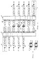
- FIG. 1 shows the circuit arrangement according to the invention with ten input modules and in Fig. 2 the possible connections of the circuit board connector are shown.
- the input modules 1 for the voltage signals all of which have the same structure, consist of a voltage converter 8, to which an adaptation circuit 9 is connected and which is followed by a low-pass filter 10.
- the input modules 2 for the current signals are also all constructed identically and consist of a current converter 11 which is connected on the secondary side to a current-voltage converter circuit 12 to which a low-pass filter 13 is connected.
- Two input modules 1 for the voltage signals and two input modules 2 for the current signals are each connected to two constant current sources 3 at the output.
- the constant current sources 3 of an input module 1, 2 are each connected to a microcomputer 4, 5.
- circuit board connectors 14 Three input modules 1 for the voltage signals and three input modules 2 for the current signals are connected to circuit board connectors 14.
- the four possible plug connections can be seen in FIG. 2.
- an input module 1, 2 can thus be connected to both microcomputers 4, 5, or the one input module 1 can be connected to one and the other input module 2 to the other microcomputer 4, 5 or vice versa.
- the circuit board connectors 14 are connected to the microcomputers 4, 5 via constant current sources 3. Since the circuit arrangement is usually arranged on a single circuit board, the connection is made for ease of service and for reasons of clarity realized between the constant current sources 3 and the microcomputers 4, 5 with ribbon cable 15.
Landscapes
- Physics & Mathematics (AREA)
- General Physics & Mathematics (AREA)
- Electronic Switches (AREA)
- Logic Circuits (AREA)
- Amplifiers (AREA)
- Power Sources (AREA)
- Microcomputers (AREA)
- Networks Using Active Elements (AREA)
- Electrophonic Musical Instruments (AREA)
Claims (4)
- Circuit pour la préparation de signaux analogiques d'intensité et de tension, pour le retraitement dans des micro-ordinateurs, caractérisé en ce qu'au moins deux modules d'entrée (1) sont prévus pour la préparation de signaux de tension et au moins deux modules d'entrée (2) sont prévus pour la préparation de signaux d'intensité, dont au moins chaque fois un module d'entrée (1, 2) est relié, par l'intermédiaire de deux sources de courant continu (3), à deux micro-ordinateurs (4, 5), et en ce que, à la sortie de l'autre module d'entrée (1, 2), sont respectivement disposées deux liaisons (6, 7) déconnectables, qui sont des prises pour plaquettes à circuit imprimé (14), des interrupteurs monopolaires de plaquettes à circuit imprimé, par exemple des interrupteurs dual-in-line, ou des interrupteurs électroniques monopolaires, par l'intermédiaire desquels soit au moins un module entrée (1; 2) peut être raccordé, avec interposition de deux sources de courant continu (3), aux deux micro-ordinateurs (4, 5), soit au moins un module d'entrée (1), destiné aux signaux de tension, peut être relié à un premier micro-ordinateur (4) et au moins un module d'entrée (2), destiné aux signaux d'intensité, peut être relié à l'autre micro-ordinateur (5), chaque fois par l'intermédiaire d'une source de courant continu (3), et en ce que le nombre des entrées des deux micro-ordinateurs (4, 5) est égal, cependant toujours inférieur au nombre de tous les modules d'entrée (1; 2), et en ce que le nombre des sources de courant continu (3) correspond à la somme des entrées des deux micro-ordinateurs (4, 5), et en ce que les modules d'entrée (1, 2), les liaisons (6, 7) déconnectables et les sources de courant continu (3) sont disposées sur une plaquette à circuit imprimé.
- Circuit selon la revendication 1, caractérisé en ce que les modules d'entrée (1) destinés aux signaux de tension sont constitués d'un convertisseur de tension (8), d'un circuit d'adaptation (9) branché en aval de celui-ci et suivi par un filtre passe-bas (10), et en ce que les modules d'entrée (2) destinés aux signaux d'intensité sont constitués d'un convertisseur d'intensité (11), auquel est raccordé un circuit convertisseur intensité-tension, avec adaptation à l'aide d'un filtre passe-bas (13) subséquent.
- Circuit selon la revendication 1 ou 2, caractérisé en ce que, au lieu respectivement de quatre liaisons (6, 7) déconnectables, deux venant d'un module d'entrée (1) pour les signaux de tension et deux venant d'un module d'entrée (2) pour les signaux d'intensité, il est prévu un interrupteur bipolaire à quatre niveaux de commutation, pour lequel chaque raccordement de racine est relié à une source de courant continu (3) dont chacune est reliée à un micro-ordinateur (4, 5), et en ce que, dans la première position d'interrupteur, le module d'entrée (1) destiné aux signaux de tension est relié aux deux micro-ordinateurs (4, 5), dans la deuxième position d'interrupteur, le module d'entrée (2) destiné aux signaux d'intensité est relié aux deux micro-ordinateurs (4, 5), dans la troisième position d'interrupteur, un premier module d'entrée (1) est relié à un micro-ordinateur (4) et l'autre module d'entrée (2) est relié à l'autre micro-ordinateur (5) et, dans la quatrième position d'interrupteur, les modules d'entrée (1, 2) et les micro-ordinateurs (4, 5) sont reliés ensemble dans l'ordre de succession inverse.
- Circuit selon l'une des revendications 1 à 3, caractérisé en ce que les deux micro-ordinateurs (4, 5) sont reliés aux sources de courant continu (3) chaque fois par l'intermédiaire d'un câble ruban plat (15), à l'aide de prises à broches multipolaires.
Applications Claiming Priority (3)
| Application Number | Priority Date | Filing Date | Title |
|---|---|---|---|
| AT0227292A AT402459B (de) | 1992-11-17 | 1992-11-17 | Schaltungsanordnung zur aufbereitung von analogen strom- und spannungssignalen |
| AT2272/92 | 1992-11-17 | ||
| PCT/AT1993/000175 WO1994011707A1 (fr) | 1992-11-17 | 1993-11-17 | Circuit pour le traitement de signaux analogiques de courant et de tension |
Publications (2)
| Publication Number | Publication Date |
|---|---|
| EP0670033A1 EP0670033A1 (fr) | 1995-09-06 |
| EP0670033B1 true EP0670033B1 (fr) | 1997-01-15 |
Family
ID=3531267
Family Applications (1)
| Application Number | Title | Priority Date | Filing Date |
|---|---|---|---|
| EP93924428A Expired - Lifetime EP0670033B1 (fr) | 1992-11-17 | 1993-11-17 | Circuit pour le traitement de signaux analogiques de courant et de tension |
Country Status (7)
| Country | Link |
|---|---|
| EP (1) | EP0670033B1 (fr) |
| CN (1) | CN1044405C (fr) |
| AT (2) | AT402459B (fr) |
| DE (1) | DE59305182D1 (fr) |
| FI (1) | FI952374A7 (fr) |
| NO (1) | NO311108B1 (fr) |
| WO (1) | WO1994011707A1 (fr) |
Families Citing this family (3)
| Publication number | Priority date | Publication date | Assignee | Title |
|---|---|---|---|---|
| DE19719633C2 (de) * | 1997-05-09 | 2000-03-30 | Daimler Chrysler Ag | Meßwertaufbereitungssystem |
| DE10100381C2 (de) * | 2001-01-05 | 2002-12-12 | Man B & W Diesel Ag | Klemmbox für einen Sensoranschluß innerhalb eines Anschlußkonzepts für Meßverstärker |
| CN115420940B (zh) * | 2022-11-04 | 2023-03-03 | 山东恒美电子科技有限公司 | 一种多用途的直流信号检测系统 |
Family Cites Families (4)
| Publication number | Priority date | Publication date | Assignee | Title |
|---|---|---|---|---|
| US4278940A (en) * | 1979-04-25 | 1981-07-14 | General Electric Company | Means for automatically compensating DC magnetization in a transformer |
| JPS6252870A (ja) * | 1985-08-30 | 1987-03-07 | デユポン ジヤパン リミテツド | 短絡コネクタ |
| US4711757A (en) * | 1986-02-27 | 1987-12-08 | Westinghouse Electric Corp. | Position indicating device |
| DE3709805A1 (de) * | 1987-03-25 | 1988-10-13 | Kloeckner Moeller Elektrizit | Verarbeitungsmodul zur erfassung analoger eingangsgroessen, insbesondere fuer mikroprozessorsysteme und speicherprogrammierbare steuerungen |
-
1992
- 1992-11-17 AT AT0227292A patent/AT402459B/de not_active IP Right Cessation
-
1993
- 1993-11-17 EP EP93924428A patent/EP0670033B1/fr not_active Expired - Lifetime
- 1993-11-17 WO PCT/AT1993/000175 patent/WO1994011707A1/fr not_active Ceased
- 1993-11-17 DE DE59305182T patent/DE59305182D1/de not_active Expired - Fee Related
- 1993-11-17 CN CN93120543A patent/CN1044405C/zh not_active Expired - Fee Related
- 1993-11-17 AT AT93924428T patent/ATE147851T1/de not_active IP Right Cessation
-
1995
- 1995-05-16 FI FI952374A patent/FI952374A7/fi unknown
- 1995-05-16 NO NO19951938A patent/NO311108B1/no not_active IP Right Cessation
Also Published As
| Publication number | Publication date |
|---|---|
| WO1994011707A1 (fr) | 1994-05-26 |
| FI952374A0 (fi) | 1995-05-16 |
| EP0670033A1 (fr) | 1995-09-06 |
| NO951938D0 (no) | 1995-05-16 |
| NO311108B1 (no) | 2001-10-08 |
| FI952374A7 (fi) | 1995-05-16 |
| AT402459B (de) | 1997-05-26 |
| CN1044405C (zh) | 1999-07-28 |
| ATA227292A (de) | 1996-09-15 |
| DE59305182D1 (de) | 1997-02-27 |
| ATE147851T1 (de) | 1997-02-15 |
| CN1091213A (zh) | 1994-08-24 |
| NO951938L (no) | 1995-05-16 |
Similar Documents
| Publication | Publication Date | Title |
|---|---|---|
| EP0712267B1 (fr) | Installation de commande modulaire avec connexion sur bus secteur intégré | |
| EP0546455B1 (fr) | Unité de commande électronique pour commuter plusieurs charges électriques | |
| DE3805593A1 (de) | Tasteneingabevorrichtung | |
| DE3510820C2 (fr) | ||
| DE2717372C3 (de) | Baugruppe aus einem Digitalschalter und elektronischen Bauelementen | |
| CH640938A5 (de) | Elektronisches geraet nach dem baukastenprinzip zur verarbeitung einer mehrzahl von simultanen messsignalen, insbesondere zur verwendung bei der ueberpruefung von geometrischen abmessungen. | |
| DE2547323C3 (de) | Trägerplatte für wenigstens eine integrierte Halbleitershaltung | |
| EP0670033B1 (fr) | Circuit pour le traitement de signaux analogiques de courant et de tension | |
| DE69121828T2 (de) | Digital-Analogwandler | |
| EP0939976B1 (fr) | Dispositif de codage de prises de fiches | |
| DE69120142T2 (de) | Zusammengesetzte elektrische Bauteile | |
| DE4032370A1 (de) | Schaltungsanordnung mit wenigstens zwei identischen, integrierten schaltungen oder schaltungsmodulen | |
| DE69203110T2 (de) | Vorrichtung zum Verbinden der Kontaktstifte eines in einem dual-in-line (DIL) Gehäuse montierten integrierten Schaltkreises mit gedruckten Schaltungen auf einer Leiterplatte auf n verschiedene Weisen. | |
| DE4013815C2 (de) | Steuerschaltung für Maschinen | |
| EP0249907B1 (fr) | Système de boîtier pour appareils électriques | |
| DE3008262C2 (de) | Elektronische Schaltungsanordnung | |
| EP0940066B1 (fr) | Dispositif de codage d'unites enfichables et dispositif de connexion de lignes exterieures au moyen d'un tel dispositif de codage | |
| EP0888707B1 (fr) | Module avec ensemble de circuits | |
| EP0177804B1 (fr) | Circuit d'alimentation en courant pour une tablette de numérisation | |
| EP0740235B1 (fr) | Système périphérique | |
| DE4413457C2 (de) | Anschlußeinheit eines Automatisierungssystems und hierzu korrespondierender Klemmenblock | |
| DE3641528C2 (fr) | ||
| DE3011564C2 (de) | Programmträger zum Programmieren von Steuerfunktionen | |
| DE2154275A1 (de) | Einrichtung zur spannungsversorgung | |
| DE9203297U1 (de) | Anordnung zur Meßbereichsanpassung |
Legal Events
| Date | Code | Title | Description |
|---|---|---|---|
| PUAI | Public reference made under article 153(3) epc to a published international application that has entered the european phase |
Free format text: ORIGINAL CODE: 0009012 |
|
| 17P | Request for examination filed |
Effective date: 19950413 |
|
| AK | Designated contracting states |
Kind code of ref document: A1 Designated state(s): AT CH DE ES FR IT LI SE |
|
| GRAG | Despatch of communication of intention to grant |
Free format text: ORIGINAL CODE: EPIDOS AGRA |
|
| 17Q | First examination report despatched |
Effective date: 19960326 |
|
| GRAH | Despatch of communication of intention to grant a patent |
Free format text: ORIGINAL CODE: EPIDOS IGRA |
|
| GRAH | Despatch of communication of intention to grant a patent |
Free format text: ORIGINAL CODE: EPIDOS IGRA |
|
| GRAA | (expected) grant |
Free format text: ORIGINAL CODE: 0009210 |
|
| AK | Designated contracting states |
Kind code of ref document: B1 Designated state(s): AT CH DE ES FR IT LI SE |
|
| PG25 | Lapsed in a contracting state [announced via postgrant information from national office to epo] |
Ref country code: IT Free format text: LAPSE BECAUSE OF FAILURE TO SUBMIT A TRANSLATION OF THE DESCRIPTION OR TO PAY THE FEE WITHIN THE PRESCRIBED TIME-LIMIT;WARNING: LAPSES OF ITALIAN PATENTS WITH EFFECTIVE DATE BEFORE 2007 MAY HAVE OCCURRED AT ANY TIME BEFORE 2007. THE CORRECT EFFECTIVE DATE MAY BE DIFFERENT FROM THE ONE RECORDED. Effective date: 19970115 Ref country code: FR Effective date: 19970115 Ref country code: ES Free format text: THE PATENT HAS BEEN ANNULLED BY A DECISION OF A NATIONAL AUTHORITY Effective date: 19970115 |
|
| REF | Corresponds to: |
Ref document number: 147851 Country of ref document: AT Date of ref document: 19970215 Kind code of ref document: T |
|
| REG | Reference to a national code |
Ref country code: CH Ref legal event code: EP |
|
| REF | Corresponds to: |
Ref document number: 59305182 Country of ref document: DE Date of ref document: 19970227 |
|
| EN | Fr: translation not filed | ||
| PLBE | No opposition filed within time limit |
Free format text: ORIGINAL CODE: 0009261 |
|
| STAA | Information on the status of an ep patent application or granted ep patent |
Free format text: STATUS: NO OPPOSITION FILED WITHIN TIME LIMIT |
|
| 26N | No opposition filed | ||
| PGFP | Annual fee paid to national office [announced via postgrant information from national office to epo] |
Ref country code: SE Payment date: 20001030 Year of fee payment: 8 |
|
| PG25 | Lapsed in a contracting state [announced via postgrant information from national office to epo] |
Ref country code: SE Free format text: LAPSE BECAUSE OF NON-PAYMENT OF DUE FEES Effective date: 20011118 |
|
| EUG | Se: european patent has lapsed |
Ref document number: 93924428.1 |
|
| PGFP | Annual fee paid to national office [announced via postgrant information from national office to epo] |
Ref country code: DE Payment date: 20021024 Year of fee payment: 10 |
|
| PGFP | Annual fee paid to national office [announced via postgrant information from national office to epo] |
Ref country code: CH Payment date: 20021028 Year of fee payment: 10 |
|
| PGFP | Annual fee paid to national office [announced via postgrant information from national office to epo] |
Ref country code: AT Payment date: 20021029 Year of fee payment: 10 |
|
| PG25 | Lapsed in a contracting state [announced via postgrant information from national office to epo] |
Ref country code: AT Free format text: LAPSE BECAUSE OF NON-PAYMENT OF DUE FEES Effective date: 20031117 |
|
| PG25 | Lapsed in a contracting state [announced via postgrant information from national office to epo] |
Ref country code: LI Free format text: LAPSE BECAUSE OF NON-PAYMENT OF DUE FEES Effective date: 20031130 Ref country code: CH Free format text: LAPSE BECAUSE OF NON-PAYMENT OF DUE FEES Effective date: 20031130 |
|
| PG25 | Lapsed in a contracting state [announced via postgrant information from national office to epo] |
Ref country code: DE Free format text: LAPSE BECAUSE OF NON-PAYMENT OF DUE FEES Effective date: 20040602 |
|
| REG | Reference to a national code |
Ref country code: CH Ref legal event code: PL |