EP0670664A1 - Energieeinsparung in einem Funkrufempfänger - Google Patents
Energieeinsparung in einem Funkrufempfänger Download PDFInfo
- Publication number
- EP0670664A1 EP0670664A1 EP94102803A EP94102803A EP0670664A1 EP 0670664 A1 EP0670664 A1 EP 0670664A1 EP 94102803 A EP94102803 A EP 94102803A EP 94102803 A EP94102803 A EP 94102803A EP 0670664 A1 EP0670664 A1 EP 0670664A1
- Authority
- EP
- European Patent Office
- Prior art keywords
- signal
- time
- rise
- receiving
- paging receiver
- Prior art date
- Legal status (The legal status is an assumption and is not a legal conclusion. Google has not performed a legal analysis and makes no representation as to the accuracy of the status listed.)
- Granted
Links
- 230000010355 oscillation Effects 0.000 claims description 2
- 230000003247 decreasing effect Effects 0.000 abstract description 2
- 230000000087 stabilizing effect Effects 0.000 description 14
- 239000003990 capacitor Substances 0.000 description 5
- 238000010586 diagram Methods 0.000 description 3
- 238000010276 construction Methods 0.000 description 1
- 238000012986 modification Methods 0.000 description 1
- 230000004048 modification Effects 0.000 description 1
- 230000000630 rising effect Effects 0.000 description 1
- 230000001629 suppression Effects 0.000 description 1
Images


Classifications
-
- H—ELECTRICITY
- H04—ELECTRIC COMMUNICATION TECHNIQUE
- H04B—TRANSMISSION
- H04B1/00—Details of transmission systems, not covered by a single one of groups H04B3/00 - H04B13/00; Details of transmission systems not characterised by the medium used for transmission
- H04B1/06—Receivers
- H04B1/16—Circuits
- H04B1/1607—Supply circuits
- H04B1/1615—Switching on; Switching off, e.g. remotely
-
- H—ELECTRICITY
- H04—ELECTRIC COMMUNICATION TECHNIQUE
- H04W—WIRELESS COMMUNICATION NETWORKS
- H04W52/00—Power management, e.g. Transmission Power Control [TPC] or power classes
- H04W52/02—Power saving arrangements
- H04W52/0209—Power saving arrangements in terminal devices
- H04W52/0261—Power saving arrangements in terminal devices managing power supply demand, e.g. depending on battery level
- H04W52/0274—Power saving arrangements in terminal devices managing power supply demand, e.g. depending on battery level by switching on or off the equipment or parts thereof
- H04W52/028—Power saving arrangements in terminal devices managing power supply demand, e.g. depending on battery level by switching on or off the equipment or parts thereof switching on or off only a part of the equipment circuit blocks
- H04W52/0283—Power saving arrangements in terminal devices managing power supply demand, e.g. depending on battery level by switching on or off the equipment or parts thereof switching on or off only a part of the equipment circuit blocks with sequential power up or power down of successive circuit blocks, e.g. switching on the local oscillator before RF or mixer stages
-
- H—ELECTRICITY
- H04—ELECTRIC COMMUNICATION TECHNIQUE
- H04W—WIRELESS COMMUNICATION NETWORKS
- H04W88/00—Devices specially adapted for wireless communication networks, e.g. terminals, base stations or access point devices
- H04W88/02—Terminal devices
- H04W88/022—Selective call receivers
-
- Y—GENERAL TAGGING OF NEW TECHNOLOGICAL DEVELOPMENTS; GENERAL TAGGING OF CROSS-SECTIONAL TECHNOLOGIES SPANNING OVER SEVERAL SECTIONS OF THE IPC; TECHNICAL SUBJECTS COVERED BY FORMER USPC CROSS-REFERENCE ART COLLECTIONS [XRACs] AND DIGESTS
- Y02—TECHNOLOGIES OR APPLICATIONS FOR MITIGATION OR ADAPTATION AGAINST CLIMATE CHANGE
- Y02D—CLIMATE CHANGE MITIGATION TECHNOLOGIES IN INFORMATION AND COMMUNICATION TECHNOLOGIES [ICT], I.E. INFORMATION AND COMMUNICATION TECHNOLOGIES AIMING AT THE REDUCTION OF THEIR OWN ENERGY USE
- Y02D30/00—Reducing energy consumption in communication networks
- Y02D30/70—Reducing energy consumption in communication networks in wireless communication networks
Definitions
- This invention relates to a paging receiver, and more particularly to, a control apparatus for suppressing the consumption of electric power in a stabilizing power supply in a paging receiver.
- a selective call is carried out by adopting time-divisional frames provider subsequent to a preamble and a synchronization code, wherein one of the frames is assigned to a corresponding one of paging receivers.
- a voltage is applied from a stabilizing power supply to a radio receiving unit to receive a selective call signal for a period of a frame assigned to the paging receiver and a ready period preceding the period of the assigned frame.
- a RF amplifier, a local oscillator, a demodulator, etc. in the radio receiving unit start to be risen-up for an intermittent receiving operation to be followed by being applied with a voltage rising up in level during the ready period, and is stabilized to demodulate the selective call signal by being applied with a voltage completely risen-up in level during the period of the assigned frame. Consequently, the electric power consumption in the stabilizing power supply is suppressed to some extent in the paging receiver by adopting the intermittent receiving operation.
- a paging receiver comprises: a radio receiving unit for generating a demodulated signal by demodulating an intermediate frequency signal obtained by mixing a local oscillation signal generated in a local oscillator and a transmitted radio signal; a decoder for decoding the demodulated signal comparing the ID code in the decoded signal with the one in the ID-ROM, and generating the alert signal if they are identical; means for representing information in accordance with the ID code in the decoded signal; means for detecting a rise-up time of the local oscillator; and means for controlling the radio receiver unit to be turned on intermittently during the rise-up time and a prescribed selective receiving time.
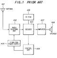
- Fig. 1 shows the conventional paging receiver which comprises a radio receiving unit 402 for receiving a signal received by an antenna 401 and generating an intermediate signal to be then demodulated therein a decoder 403 for decoding a signal demodulated in the radio receiving unit 402 to provide an ID code to be compared with an assigned ID code and generating an alert signal in accordance with the coincident of the ID codes, a control unit 404 for generating a control signal by receiving a synchronization code from the decoder 403, a stabilizing power supply 405 for applying a voltage to the radio receiving unit 402 by receiving the control signal from the control unit 404, an ID-ROM storing an ID-code assigned to the paging receiver, and an amplifier 407 for amplifying the alert signal supplied from the decoder 403 and supplying the amplified alert signal to a speaker 408.
- a radio receiving unit 402 for receiving a signal received by an antenna 401 and generating an intermediate signal to be then demodulated therein a decoder 40
- Radio Paging Code No. 1 which is adopted in CCIR REQ584-1 is used in the paging receiver.
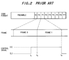
- a transmitted signal of a code format as shown in Fig. 2 is supplied from the antenna 401 to the radio receiving unit 402, in which the transmitted signal is demodulated in accordance with a voltage intermittently supplied from the stabilizing power supply 405 thereto, so that a preamble PA of 576 bits and a synchronization code SC of 32 bits are decoded in the decoder 403 in accordance with the demodulated signal supplied from the radio receiving unit 402.
- the preamble PA and the synchronization code SC are supplied from the decoder 403 to the control unit 404, so that the bit synchronization is set up by the preamble PA, and the frame synchronization is set up by the synchronism signal SC.
- frames F0 to F7 are transmitted, wherein the frame F1 is assigned to the paging receiver as shown in Fig. 2.
- a control signal having a fixed ready period (t1 to t2) and an intermittent receiving operation period (t2 to t3) as shown in Fig. 2 is supplied from the control unit 404 to the stabilizing control unit 405, so that a voltage is applied from the stabilizing power supply 405 to the radio receiving unit 402 during the high state (t1 to t3) of the control signal.
- a power supply voltage is risen-up to be applied to a RF amplifier, a local oscillator, a demodulator, etc. in the radio receiving unit 402 during the ready period (t1 to t2), so that a selective call signal of the frame F1 is demodulated in the radio receiving unit 402 during the operation period (t2 to t3).
- the demodulated selective call signal is then supplied to the decoder 403 during that period, and is decoded therein to provide the transmitted ID code which is then compared with the assigned ID code read from the ID-ROM 406.
- an alert signal is generated in the decoder 403, and the alert signal is supplied to the amplifier 407, from which the amplified alert signal is supplied to the speaker 408.
- alert sound is generated for a user carrying the paging receiver by the speaker 408.
- the ready period (t1 to t2) is fixed to have an appropriate margin of time common to paging receivers having different rising-up properties.
- the aforementioned disadvantage is observed in the conventional paging receiver.
- Fig. 3 shows the paging receiver which comprises a radio receiving unit 102 receiving a signal from an antenna 101, a decoder 103, a control unit 104, a rise-up time detecting unit 105, a stabilizing power supply 106, an ID-ROM, an amplifier 108, and a speaker 109, wherein the blocks other than the rise-up time detecting unit 105 operate in the same manner as in the conventional paging receiver in Fig. 1.
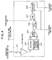
- Fig. 4 shows the rise-up time detecting unit 105 which comprises a capacitor 201 for passing an AC component of a signal supplied from the radio receiving unit 102 to remove a DC component thereof, an amplifier 202 for amplifying the AC component signal, a rectifier 203 for rectifying the amplified signal to provide a rectified signal, a reference voltage generator 204 for generating a reference voltage, a comparator 205 for comparing the rectified signal and the reference voltage, an exclusive OR circuit 206 for carrying out the logic calculation of exclusive OR between an output signal of the comparator 205 and a control signal supplied from the control unit 104, an AND circuit 207 for passing a clock signal when an output signal of the exclusive OR circuit 206 is high, and a counter 208 for counting the pulse number of the clock signal passed through the AND circuit 207 to supply the counted number to the control unit 104.
- a capacitor 201 for passing an AC component of a signal supplied from the radio receiving unit 102 to remove a DC component thereof
- an amplifier 202 for ampl
- An intermediate frequency (IF) signal A is generated in a local oscillator (not shown) in the radio receiving unit 102, and the IF signal A is supplied to the capacitor 201 in the rise-up time detecting unit 105, so that the capacitor signal B which is an AC component of the IF signal A is supplied from the capacitor 201.
- the capacitor signal B is amplified in the amplifier 202, from which an amplified signal C is supplied to the rectifier 203, so that the rectified signal D is supplied to the first input of the comparator 205, to the second input of which a reference voltage E is supplied from the reference voltage generator 204.
- a comparator signal F which is high at the time when the rectified signal D is greater than the reference voltage E is supplied from the comparator 205.
- the comparator signal F and the control signal G supplied from the control unit 104 are supplied to the exclusive OR circuit 206, so that an exclusive OR signal H is generated therein.
- the exclusive OR signal is high, when the control signal G is high, and the comparator signal F is low.
- the exclusive OR signal H is supplied to the AND circuit 207, so that the clock signal I is passed through the AND circuit 207 to be supplied to the counter 208 as an AND signal J, when the exclusive OR signal H is high.
- the pulse number of the AND signal J is counted in the counter 208.
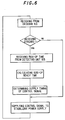
- the counted number is a rise-up time signal to be supplied to the control unit 104, in which a timing of supplying the control signal G to the stabilizing power supply 106 (and also to the rise-up time detecting circuit 105) is determined in accordance with the rise-up time (the counted number) and a setting-up timing of the frame synchronization.
- the control unit 104 receives a signal representing the setting-up timing of the frame synchronization from the decoder 103, in which the synchronization signal SC is decoded. Then, the control unit 104 receives the rise-up time (the counted number) from the rise-up time detecting unit 105. Thus, a ready period (corresponding to a period of t1 to t2 in Fig. 2) of the control signal G is calculated in the control unit 104 by using the rise-up time. Then, a timing of supplying the control signal G having the calculated ready period to the stabilizing power supply 105 is determined in the control unit 104 in accordance with the setting-up timing of the frame synchronization and the ready period of the control signal G.
- a frame in which an intermittent receiving operation is carried out is determined on the basis of the setting-up timing of the frame synchronization, and a timing of supplying the control signal G to the stabilizing power supply 106 is determined in consideration of the calculated ready period of the control signal G and a start timing of the determined frame.
- the electric power consumption of a battery in the stabilizing power supply 106 is decreased, because a timing of supplying the control signal G from the control unit 104 to the stabilizing power supply 106, that is, a turning-on timing of a RF amplifier, a local oscillator, a demodulator, etc. in the radio receiving unit 102 is determined at each time by detecting an actual rise-up time of the radio receiving unit 102, for instance, the local oscillator.
Landscapes
- Engineering & Computer Science (AREA)
- Computer Networks & Wireless Communication (AREA)
- Signal Processing (AREA)
- Mobile Radio Communication Systems (AREA)
- Circuits Of Receivers In General (AREA)
Priority Applications (6)
| Application Number | Priority Date | Filing Date | Title |
|---|---|---|---|
| EP94102803A EP0670664B1 (de) | 1994-02-24 | 1994-02-24 | Energieeinsparung in einem Funkrufempfänger |
| DE1994613201 DE69413201T2 (de) | 1994-02-24 | 1994-02-24 | Energieeinsparung in einem Funkrufempfänger |
| AU56409/94A AU673572B2 (en) | 1994-02-24 | 1994-02-25 | Paging receiver |
| CA002116477A CA2116477C (en) | 1994-02-24 | 1994-02-25 | A power saving paging receiver |
| US08/202,063 US5473319A (en) | 1994-02-24 | 1994-02-25 | Paging receiver |
| CN94104080A CN1035915C (zh) | 1994-02-24 | 1994-02-26 | 寻呼接收机 |
Applications Claiming Priority (5)
| Application Number | Priority Date | Filing Date | Title |
|---|---|---|---|
| EP94102803A EP0670664B1 (de) | 1994-02-24 | 1994-02-24 | Energieeinsparung in einem Funkrufempfänger |
| AU56409/94A AU673572B2 (en) | 1994-02-24 | 1994-02-25 | Paging receiver |
| CA002116477A CA2116477C (en) | 1994-02-24 | 1994-02-25 | A power saving paging receiver |
| US08/202,063 US5473319A (en) | 1994-02-24 | 1994-02-25 | Paging receiver |
| CN94104080A CN1035915C (zh) | 1994-02-24 | 1994-02-26 | 寻呼接收机 |
Publications (2)
| Publication Number | Publication Date |
|---|---|
| EP0670664A1 true EP0670664A1 (de) | 1995-09-06 |
| EP0670664B1 EP0670664B1 (de) | 1998-09-09 |
Family
ID=27507079
Family Applications (1)
| Application Number | Title | Priority Date | Filing Date |
|---|---|---|---|
| EP94102803A Expired - Lifetime EP0670664B1 (de) | 1994-02-24 | 1994-02-24 | Energieeinsparung in einem Funkrufempfänger |
Country Status (5)
| Country | Link |
|---|---|
| US (1) | US5473319A (de) |
| EP (1) | EP0670664B1 (de) |
| CN (1) | CN1035915C (de) |
| AU (1) | AU673572B2 (de) |
| CA (1) | CA2116477C (de) |
Cited By (2)
| Publication number | Priority date | Publication date | Assignee | Title |
|---|---|---|---|---|
| EP0863636A3 (de) * | 1997-03-05 | 2002-07-31 | Northrop Grumman Corporation | Adaptive Schlafschaltung mit Netzwerk-Zeitsignalrückführung |
| DE10115343A1 (de) * | 2001-03-28 | 2002-10-10 | Philips Corp Intellectual Pty | Pager-System |
Families Citing this family (4)
| Publication number | Priority date | Publication date | Assignee | Title |
|---|---|---|---|---|
| JP2611670B2 (ja) * | 1994-07-25 | 1997-05-21 | 日本電気株式会社 | 選択呼出受信機 |
| CN1102325C (zh) * | 1995-12-04 | 2003-02-26 | 摩托罗拉公司 | 混合系统环境中动态改变选择呼叫接收设备控制帧的方法 |
| US6236850B1 (en) | 1999-01-08 | 2001-05-22 | Trw Inc. | Apparatus and method for remote convenience function control with increased effective receiver seek time and reduced power consumption |
| CN101361280B (zh) | 2006-01-17 | 2013-05-01 | 艾利森电话股份有限公司 | 用于减少移动通信网络中的功耗的方法和设备 |
Citations (1)
| Publication number | Priority date | Publication date | Assignee | Title |
|---|---|---|---|---|
| WO1991019357A1 (en) * | 1990-06-04 | 1991-12-12 | Motorola, Inc. | Battery saving method and apparatus for providing selective receiver power switching |
Family Cites Families (1)
| Publication number | Priority date | Publication date | Assignee | Title |
|---|---|---|---|---|
| JPH02261226A (ja) * | 1989-03-31 | 1990-10-24 | Mitsubishi Electric Corp | 移動電話機 |
-
1994
- 1994-02-24 EP EP94102803A patent/EP0670664B1/de not_active Expired - Lifetime
- 1994-02-25 CA CA002116477A patent/CA2116477C/en not_active Expired - Fee Related
- 1994-02-25 AU AU56409/94A patent/AU673572B2/en not_active Ceased
- 1994-02-25 US US08/202,063 patent/US5473319A/en not_active Expired - Fee Related
- 1994-02-26 CN CN94104080A patent/CN1035915C/zh not_active Expired - Fee Related
Patent Citations (1)
| Publication number | Priority date | Publication date | Assignee | Title |
|---|---|---|---|---|
| WO1991019357A1 (en) * | 1990-06-04 | 1991-12-12 | Motorola, Inc. | Battery saving method and apparatus for providing selective receiver power switching |
Cited By (2)
| Publication number | Priority date | Publication date | Assignee | Title |
|---|---|---|---|---|
| EP0863636A3 (de) * | 1997-03-05 | 2002-07-31 | Northrop Grumman Corporation | Adaptive Schlafschaltung mit Netzwerk-Zeitsignalrückführung |
| DE10115343A1 (de) * | 2001-03-28 | 2002-10-10 | Philips Corp Intellectual Pty | Pager-System |
Also Published As
| Publication number | Publication date |
|---|---|
| CA2116477C (en) | 2000-01-11 |
| CA2116477A1 (en) | 1995-08-26 |
| CN1035915C (zh) | 1997-09-17 |
| CN1107626A (zh) | 1995-08-30 |
| AU5640994A (en) | 1995-09-28 |
| AU673572B2 (en) | 1996-11-14 |
| US5473319A (en) | 1995-12-05 |
| EP0670664B1 (de) | 1998-09-09 |
Similar Documents
| Publication | Publication Date | Title |
|---|---|---|
| KR860000638B1 (ko) | 배터리 절약회로를 개량시킨 선택호출수신기 | |
| JP3110173B2 (ja) | 無線選択呼出受信機の受信制御方式 | |
| KR900009178B1 (ko) | 바테리 절약 회로를 갖고 있는 페이징 수신기 | |
| RU2110889C1 (ru) | Устройство для управления потреблением мощности радиоприемника и способ управления радиоприемником в системе радиосвязи | |
| KR0160366B1 (ko) | 무선기의 간헐적 수신 타이밍을 제어하는 회로 및 방법 | |
| US6195571B1 (en) | Electronic apparatus capable of automatically switching notification devices | |
| KR0148651B1 (ko) | 비연속적인 수신 모드에서 동작하는 수신기에 대한 턴온 시간을 최소화하는 장치 및 방법 | |
| JP3076226B2 (ja) | 不連続受信モードで動作する受信機のためのターンオン時間を最小化する装置および方法 | |
| KR100219106B1 (ko) | 전원-오프 상태에서 신호 수신을 제공하는 수신기 | |
| JPH0799476A (ja) | 無線通信装置におけるバッテリ節約方法および装置 | |
| US6304761B1 (en) | Mobile unit communication apparatus having digital and analog communication modes and a method of controlling the same | |
| US5473319A (en) | Paging receiver | |
| EP0568856B1 (de) | Pagingreceiver mit Detektion der Daten-Geschwindigkeit zur Fortsetzung des Empfangs der Adressdaten | |
| EP0301871B1 (de) | Selektiv-Rufempfänger | |
| KR100203609B1 (ko) | 전원 전압 검출 기능을 갖는 무선 선택 호출 수신기 | |
| GB2278004A (en) | Selective power supply control | |
| HK1014131A1 (en) | Power-saving in a paging receiver | |
| HK1014131B (en) | Power-saving in a paging receiver | |
| JP2710554B2 (ja) | 無線選択呼出し受信機のバッテリセービング方式 | |
| US5452472A (en) | Radio communication receiving device detecting a frequency modulation preamble signal | |
| JP3080632B2 (ja) | 無線選択呼出受信機 | |
| GB1561917A (en) | Selectively callable receiving apparatus | |
| KR100252558B1 (ko) | 2진 부호 전송시 소비전력 감소 모드를 갖는 가변 포맷의 무선 페이저 | |
| US5666657A (en) | Method in a selective call receiver for applying conditional partial address correlation to a message | |
| EP0936757A4 (de) | Vorrichtung und verfahren zur funkkommunikation |
Legal Events
| Date | Code | Title | Description |
|---|---|---|---|
| PUAI | Public reference made under article 153(3) epc to a published international application that has entered the european phase |
Free format text: ORIGINAL CODE: 0009012 |
|
| 17P | Request for examination filed |
Effective date: 19940727 |
|
| AK | Designated contracting states |
Kind code of ref document: A1 Designated state(s): DE GB NL |
|
| GRAG | Despatch of communication of intention to grant |
Free format text: ORIGINAL CODE: EPIDOS AGRA |
|
| 17Q | First examination report despatched |
Effective date: 19970901 |
|
| GRAG | Despatch of communication of intention to grant |
Free format text: ORIGINAL CODE: EPIDOS AGRA |
|
| GRAG | Despatch of communication of intention to grant |
Free format text: ORIGINAL CODE: EPIDOS AGRA |
|
| GRAH | Despatch of communication of intention to grant a patent |
Free format text: ORIGINAL CODE: EPIDOS IGRA |
|
| GRAH | Despatch of communication of intention to grant a patent |
Free format text: ORIGINAL CODE: EPIDOS IGRA |
|
| GRAA | (expected) grant |
Free format text: ORIGINAL CODE: 0009210 |
|
| AK | Designated contracting states |
Kind code of ref document: B1 Designated state(s): DE GB NL |
|
| REF | Corresponds to: |
Ref document number: 69413201 Country of ref document: DE Date of ref document: 19981015 |
|
| PLBE | No opposition filed within time limit |
Free format text: ORIGINAL CODE: 0009261 |
|
| STAA | Information on the status of an ep patent application or granted ep patent |
Free format text: STATUS: NO OPPOSITION FILED WITHIN TIME LIMIT |
|
| 26N | No opposition filed | ||
| PGFP | Annual fee paid to national office [announced via postgrant information from national office to epo] |
Ref country code: NL Payment date: 20010228 Year of fee payment: 8 |
|
| REG | Reference to a national code |
Ref country code: GB Ref legal event code: IF02 |
|
| PG25 | Lapsed in a contracting state [announced via postgrant information from national office to epo] |
Ref country code: NL Free format text: LAPSE BECAUSE OF NON-PAYMENT OF DUE FEES Effective date: 20020901 |
|
| NLV4 | Nl: lapsed or anulled due to non-payment of the annual fee |
Effective date: 20020901 |
|
| PGFP | Annual fee paid to national office [announced via postgrant information from national office to epo] |
Ref country code: GB Payment date: 20040218 Year of fee payment: 11 |
|
| PGFP | Annual fee paid to national office [announced via postgrant information from national office to epo] |
Ref country code: DE Payment date: 20040304 Year of fee payment: 11 |
|
| PG25 | Lapsed in a contracting state [announced via postgrant information from national office to epo] |
Ref country code: GB Free format text: LAPSE BECAUSE OF NON-PAYMENT OF DUE FEES Effective date: 20050224 |
|
| PG25 | Lapsed in a contracting state [announced via postgrant information from national office to epo] |
Ref country code: DE Free format text: LAPSE BECAUSE OF NON-PAYMENT OF DUE FEES Effective date: 20050901 |
|
| GBPC | Gb: european patent ceased through non-payment of renewal fee |
Effective date: 20050223 |