EP0671088B1 - Circuit pour la commande d'un ensemble de recepteurs, notamment de regulateurs de puissance de lampes - Google Patents
Circuit pour la commande d'un ensemble de recepteurs, notamment de regulateurs de puissance de lampes Download PDFInfo
- Publication number
- EP0671088B1 EP0671088B1 EP19940900132 EP94900132A EP0671088B1 EP 0671088 B1 EP0671088 B1 EP 0671088B1 EP 19940900132 EP19940900132 EP 19940900132 EP 94900132 A EP94900132 A EP 94900132A EP 0671088 B1 EP0671088 B1 EP 0671088B1
- Authority
- EP
- European Patent Office
- Prior art keywords
- branch
- transmitting
- circuit arrangement
- coupling unit
- arrangement according
- Prior art date
- Legal status (The legal status is an assumption and is not a legal conclusion. Google has not performed a legal analysis and makes no representation as to the accuracy of the status listed.)
- Expired - Lifetime
Links
Images



Classifications
-
- H—ELECTRICITY
- H02—GENERATION; CONVERSION OR DISTRIBUTION OF ELECTRIC POWER
- H02J—ELECTRIC POWER NETWORKS; CIRCUIT ARRANGEMENTS OR SYSTEMS FOR SUPPLYING OR DISTRIBUTING ELECTRIC POWER; SYSTEMS FOR STORING ELECTRIC ENERGY
- H02J13/00—Circuit arrangements for providing remote monitoring or remote control of equipment in a power distribution network
- H02J13/13—Circuit arrangements for providing remote monitoring or remote control of equipment in a power distribution network characterised by the transmission of data to equipment in the power network
- H02J13/1321—Circuit arrangements for providing remote monitoring or remote control of equipment in a power distribution network characterised by the transmission of data to equipment in the power network using a wired telecommunication network or a data transmission bus
-
- H—ELECTRICITY
- H05—ELECTRIC TECHNIQUES NOT OTHERWISE PROVIDED FOR
- H05B—ELECTRIC HEATING; ELECTRIC LIGHT SOURCES NOT OTHERWISE PROVIDED FOR; CIRCUIT ARRANGEMENTS FOR ELECTRIC LIGHT SOURCES, IN GENERAL
- H05B47/00—Circuit arrangements for operating light sources in general, i.e. where the type of light source is not relevant
- H05B47/10—Controlling the light source
- H05B47/175—Controlling the light source by remote control
- H05B47/18—Controlling the light source by remote control via data-bus transmission
-
- Y—GENERAL TAGGING OF NEW TECHNOLOGICAL DEVELOPMENTS; GENERAL TAGGING OF CROSS-SECTIONAL TECHNOLOGIES SPANNING OVER SEVERAL SECTIONS OF THE IPC; TECHNICAL SUBJECTS COVERED BY FORMER USPC CROSS-REFERENCE ART COLLECTIONS [XRACs] AND DIGESTS
- Y02—TECHNOLOGIES OR APPLICATIONS FOR MITIGATION OR ADAPTATION AGAINST CLIMATE CHANGE
- Y02B—CLIMATE CHANGE MITIGATION TECHNOLOGIES RELATED TO BUILDINGS, e.g. HOUSING, HOUSE APPLIANCES OR RELATED END-USER APPLICATIONS
- Y02B70/00—Technologies for an efficient end-user side electric power management and consumption
- Y02B70/30—Systems integrating technologies related to power network operation and communication or information technologies for improving the carbon footprint of the management of residential or tertiary loads, i.e. smart grids as climate change mitigation technology in the buildings sector, including also the last stages of power distribution and the control, monitoring or operating management systems at local level
-
- Y—GENERAL TAGGING OF NEW TECHNOLOGICAL DEVELOPMENTS; GENERAL TAGGING OF CROSS-SECTIONAL TECHNOLOGIES SPANNING OVER SEVERAL SECTIONS OF THE IPC; TECHNICAL SUBJECTS COVERED BY FORMER USPC CROSS-REFERENCE ART COLLECTIONS [XRACs] AND DIGESTS
- Y02—TECHNOLOGIES OR APPLICATIONS FOR MITIGATION OR ADAPTATION AGAINST CLIMATE CHANGE
- Y02B—CLIMATE CHANGE MITIGATION TECHNOLOGIES RELATED TO BUILDINGS, e.g. HOUSING, HOUSE APPLIANCES OR RELATED END-USER APPLICATIONS
- Y02B90/00—Enabling technologies or technologies with a potential or indirect contribution to GHG emissions mitigation
- Y02B90/20—Smart grids as enabling technology in buildings sector
-
- Y—GENERAL TAGGING OF NEW TECHNOLOGICAL DEVELOPMENTS; GENERAL TAGGING OF CROSS-SECTIONAL TECHNOLOGIES SPANNING OVER SEVERAL SECTIONS OF THE IPC; TECHNICAL SUBJECTS COVERED BY FORMER USPC CROSS-REFERENCE ART COLLECTIONS [XRACs] AND DIGESTS
- Y04—INFORMATION OR COMMUNICATION TECHNOLOGIES HAVING AN IMPACT ON OTHER TECHNOLOGY AREAS
- Y04S—SYSTEMS INTEGRATING TECHNOLOGIES RELATED TO POWER NETWORK OPERATION, COMMUNICATION OR INFORMATION TECHNOLOGIES FOR IMPROVING THE ELECTRICAL POWER GENERATION, TRANSMISSION, DISTRIBUTION, MANAGEMENT OR USAGE, i.e. SMART GRIDS
- Y04S20/00—Management or operation of end-user stationary applications or the last stages of power distribution; Controlling, monitoring or operating thereof
- Y04S20/20—End-user application control systems
- Y04S20/242—Home appliances
- Y04S20/246—Home appliances the system involving the remote operation of lamps or lighting equipment
-
- Y—GENERAL TAGGING OF NEW TECHNOLOGICAL DEVELOPMENTS; GENERAL TAGGING OF CROSS-SECTIONAL TECHNOLOGIES SPANNING OVER SEVERAL SECTIONS OF THE IPC; TECHNICAL SUBJECTS COVERED BY FORMER USPC CROSS-REFERENCE ART COLLECTIONS [XRACs] AND DIGESTS
- Y04—INFORMATION OR COMMUNICATION TECHNOLOGIES HAVING AN IMPACT ON OTHER TECHNOLOGY AREAS
- Y04S—SYSTEMS INTEGRATING TECHNOLOGIES RELATED TO POWER NETWORK OPERATION, COMMUNICATION OR INFORMATION TECHNOLOGIES FOR IMPROVING THE ELECTRICAL POWER GENERATION, TRANSMISSION, DISTRIBUTION, MANAGEMENT OR USAGE, i.e. SMART GRIDS
- Y04S40/00—Systems for electrical power generation, transmission, distribution or end-user application management characterised by the use of communication or information technologies, or communication or information technology specific aspects supporting them
- Y04S40/12—Systems for electrical power generation, transmission, distribution or end-user application management characterised by the use of communication or information technologies, or communication or information technology specific aspects supporting them characterised by data transport means between the monitoring, controlling or managing units and monitored, controlled or operated electrical equipment
- Y04S40/124—Systems for electrical power generation, transmission, distribution or end-user application management characterised by the use of communication or information technologies, or communication or information technology specific aspects supporting them characterised by data transport means between the monitoring, controlling or managing units and monitored, controlled or operated electrical equipment using wired telecommunication networks or data transmission busses
Definitions
- the invention relates to a circuit arrangement for controlling a plurality of consumers, such as lamps.
- a plurality of consumers such as lamps.
- each of these lamps requires its own ballast in order to supply the gas discharge lamp with the ignition or operating voltage required in each case.
- a circuit arrangement is known in which a central unit is connected via a data bus to a plurality of peripheral units whose functions are controlled via the data bus.
- Each peripheral unit has a coupling unit which is divided into a receiving branch and a transmitting branch.
- the receiving branch is used to transmit information from the central unit to the peripheral unit, the central unit delivering information to the data bus in the form of a modulated AC or pulse voltage.
- the transmission branch is used to transmit information from the peripheral unit to the central unit. The information is transferred from the peripheral unit to the data bus by varying the output resistance of the transmission branch.
- a central unit controls a large number of ballasts for gas discharge lamps via a bus.
- Each ballast is connected to the bus via a coupling unit.
- data are transmitted from the bus to the respective ballast via a capacitor circuit or by means of a transmitter. If feedback signals are to be transmitted from the ballast to the central unit, then when there is no data on the bus, it is possible to couple these signals from the ballast into the bus via the same coupling unit.
- the invention is therefore based on the object of developing a circuit arrangement for controlling a plurality of consumers of the type described at the outset in such a way that reliable operation is always ensured with minimal power consumption.
- the coupling unit has a receiving branch for the transmission of control information from the central unit which is in the transmission mode to the consumer assigned to the coupling unit, and a transmission branch for the transmission of feedback information from the consumer to the central unit which is in the non-transmission mode.
- the coupling unit also has a sleep device which puts the receiving branch into an inactive state when the central control unit is not in operation.
- an advantageous further development is that the consumers and the central unit are connected to a common bus, which means the circuitry for connecting the consumers to the central unit is minimized. Since the consumers are galvanically isolated from the bus by means of the respective coupling units, an undesired occurrence of compensating currents is avoided, the use of an optocoupler enabling the transmission of rectangular signals without having to use transmitters which are considerably more expensive to purchase.
- a further advantageous embodiment of the invention is given in that the central unit, when it does not output any data signals on the bus, outputs a signal whose voltage level is different from the voltage level of the data signals.
- an advantageous development is given in that the current consumption in the coupling device is monitored, for example, by a constant current source formed with a MOS field effect transistor, so that further employment of the circuit arrangement is avoided in the event of incorrect wiring or a defective component.
- the coupling unit has reverse polarity protection, which is formed, for example, with a rectifier bridge circuit.
- the connection of the coupling unit to the bus is simplified and, at the same time, damage to the coupling unit or the consumer is protected by incorrect connection.
- the rectifier bridge circuit has the advantage in particular in connection with the optocouplers that the coupling unit can transmit square-wave signals largely without distortion.
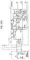
- FIG. 1 shows a block diagram in which a central unit or central control unit 5 is connected to a data bus or a data line 1. Furthermore, several coupling units 3 are connected to the data line 1, which couple the data line to the consumers 4 or their respective control unit. The signals output by the central unit 5 on the data line are thus also present at the inputs of all consumers 4. It is therefore necessary, if individual consumers are to be controlled, to code the data signals in a consumer-specific manner.
- the coupling unit has a receiving branch for a connection directed to the consumer. Analogously to the data transmission from the consumer to the data line, there is a connection directed from the consumer to the coupling unit, which forms a transmission branch.
- the central control unit 5 is connected to the data line 1 in the form of a two-wire line, the central control unit 5 having a signal generator which generates rectangular data signals which in this case have a peak level of 12 V. Furthermore, a DC voltage generator DC with an internal resistance Ri is provided, which emits a DC voltage of 4 V. Both generators generate their signals in relation to a common ground potential, to which one of the two connections of the data line 1 is also connected.
- a control switch S1 is connected with its movable working contact to the second connection of the data line 1 and is connected with its fixed selection contacts to one output of each of the two generators.
- a control unit of a consumer 4 such as an electronic ballast EVG for a gas discharge lamp, is coupled to its coupling unit 3.
- a rectifier bridge circuit BR on the device side, ie in the coupling unit 3.
- the AC voltage connections of the bridge circuit are connected to the interface, while the connections +/- to the subsequent components of the Coupling unit 3 are connected.
- a self-conducting MOS field-effect transistor T3 is connected to its drain connection to the plus connection of the bridge circuit BR.
- a resistor R3 is connected in parallel between the gate connection and the source connection.
- a series circuit consisting of a PTC thermistor RK, a Zener diode ZD1, a resistor RV and an optocoupler V2 is connected between the resistor R3 and the minus connection of the rectifier BR, the anode connection of the Zener diode ZD1 via the Resistor RV is connected to the anode connection of the transmitter diode of the optocoupler V2.
- the minus connection of the bridge rectifier BR is referred to below as the minus line.
- the second embodiment is the same as the first embodiment described above, but additionally has the circuit elements described below.
- a series circuit is connected between the node R3 / RK and the negative line, which consequently consists of a transistor T1, resistors R1 and R5 and the output of an optocoupler V1.
- the transistor T1 is connected with its collector to the positive terminal of the bridge rectifier BR and with its emitter terminal to the resistor R1.
- the collector of transistor T1 At the base terminal of transistor T1 is the collector of a transistor T2, the emitter of which is connected to the negative line.
- one terminal of a resistor R4 is connected to the collector of transistor T2, while the other terminal is connected to node RK / ZD1.
- a Zener diode ZD3 is connected to its cathode at the same node, while a resistor R6 is connected in series with its anode to the minus connection of the bridge rectifier.
- a resistor R2 is connected between the base connection of the transistor T2 and the node ZD3 / R6.
- a parallel circuit comprising a Zener diode ZD4 and a transistor T4 is connected between the node R1 / R5 and the negative line, the Zener diode with its cathode contact and the transistor T4 with its collector being connected to this node.
- the emitter of transistor T4 is connected to the negative line and the base connection at node R5 / V1.
- a Zener diode ZD2 is connected with its anode to the negative lead and with its cathode to the node RK / ZD1.
- the connections of the receiving transistor are connected to the data input lines DS and Gnd of a control unit 4 of the electronic ballast, while on the transmitting side of the optocoupler V1, the connections of the transmitting diode are connected to connections from Error feedback lines RS and Gnd of the control unit 4 of the electronic ballast are connected.
- the respective ground lines Gnd of the data line and the error feedback lines can be combined and implemented as a common ground line Gnd.
- the setting switch S1 switches over to the DC voltage generator DC, so there is no transmission mode.
- a DC voltage of, for example, 4 V is now present on the data line 1, as a result of which the electronic ballast signals that the central control unit 5 is ready to receive, the polarity of the DC voltage generator DC also being of no importance as a result of the bridge rectifier BR in the input of the control unit.
- the Zener diode ZD1 has a Zener voltage, the value of which is lower than the signal level of the data signal generator and greater than the level of the DC voltage generator DC, for example 4.7 V
- the central unit 5 of the optocoupler V2 is in non-transmission operation by means of the Zener Diode ZD1 switched off.
- the transmission diode of the optocoupler V2 thus does not consume any electrical energy, which must be supplied via the data line 1, when the central unit is in the receiving mode.
- the maximum current consumption of the coupling unit 3 is limited by the self-conducting MOS field effect transistor T3. This is inherently conductive without a signal between the gate connection and the source connection. Through a current that flows through the drain-source path and thus also through the resistor R3, a voltage drop occurs at the resistor R3, which at the same time causes a voltage signal between the gate connection and the source connection. In accordance with this signal, the conductivity of the transistor T3 is reduced, as a result of which the current consumption of the coupling unit 3 is restricted.
- This current limitation essentially serves as a safety device which is intended to prevent damage to the components in the coupling unit if an incorrectly dimensioned signal source is connected to the interface of the coupling unit 3.
- the current flow through the optocoupler V2 is limited by the resistor RV. Since a current limiting device is already provided with the MOS field effector T3, this resistance RV itself can be omitted. However, since the MOS field-effect transistor T3 serves to limit the current of the receiving transistor of the optocoupler V1 and the transmitting diode of the optocoupler V2, the use of the resistor RV is recommended on the one hand because of the differences in components and because of the strong temperature dependency of the MOS field-effect transistor T3. The same applies analogously to the resistor R1.
- the constant current source with the MOS field effect transistor T3, as shown in FIG. 3, can also be replaced by other circuit arrangements which represent constant current sources or current limiting devices.
- circuit arrangements which represent constant current sources or current limiting devices.
- the constant current source can be omitted, as indicated in FIGS. 2 and 3 by means of dashed lines, wherein the simple replacement of the constant current source by a resistor would also be conceivable.
- the Zener diode ZD3 is determined by the Zener diode ZD3 as an allowable voltage if the Zener voltage of this Zener diode is between 15 V and 20 V.
- the transistor T1 is now controlled via the resistor R4, as a result of which the voltage forwarded by the rectifier BR is present on the data line 1 between the collector and emitter of the transistor T4, which is initially blocking, via the resistor R1.
- the collector / base section of the receiving transistor of the optocoupler V1 is in reverse polarity, only the reverse current of the receiving transistor is conducted on this circuit branch, so that as long as no data are to be output from the electronic ballast into the data line, also from the optocoupler V1 does not consume any significant current to be supplied via the data line.
- a signal from the control unit of the electronic ballast via the feedback signal line RS such as an error feedback, is to be transmitted to the central control unit, these signals are sent out via the transmission diode of the optocoupler V1.
- these signals are also first converted into optical signals and then recovered as electrical signals, as a result of which the connection between the control unit 4 of the electronic ballast and the data line 1 is also galvanically isolated.
- the conductivity of the receiving transistor is modulated by the reception of the optical signal emitted by the transmission diode of the optocoupler V1, which switches the transistor T4 to conductive via the voltage drop across the resistor R5, which places a load on the DC voltage generator DC in the central control unit 5. This load is determined and evaluated in the central control unit 5 at the resistor Ri.
- the Zener diode ZD2 which has a Zener voltage of, for example, 20 Volts, short-circuited.
- the impermissibly high voltage in the receiving branch of the coupling unit 3 is derived in front of the optocoupler V2.
- voltages which are above 20 volts are therefore defined as an impermissibly high voltage.
- this definition depends entirely on the permissible limit values of the optocoupler V2, so that the Zener diode ZD2 must also be dimensioned accordingly in a differently selected optocoupler.
- the Zener diode ZD3 first recognizes that an inadmissibly high voltage is present, which makes it conductive, so that a voltage drops across the resistor R6, which voltage is supplied via the resistor R2 to the base of the transistor T2. This becomes conductive and short-circuits the base-emitter voltage of the transistor T1, so that it switches off and changes into a non-conductive state. In this way, impermissibly high voltages are kept away from the transistor T4 and the receiving transistor of the optocoupler V1 in the transmission branch of the coupling unit 3. Since the previously described switching off of the transmission branch does not take place sufficiently quickly in some cases, the Zener diode ZD4 is additionally provided for the brief occurrence of an overvoltage.
- Zener diodes When using Zener diodes as overvoltage protection, care must be taken that the Zener diode must conduct a high current when discharging an overvoltage, as a result of which a large amount of electrical energy is converted into thermal energy in the Zener diode. This can easily damage the Zener diode, which would then open the connection if it melted, which would lead to the elimination of the proposed overvoltage protection. For this reason, the PTC thermistor RK was provided in the receiving branch of the coupling unit 3, which initially has a very low resistance, but with a permanently high current flow, its resistance value increases along with its heating.
- the PTC thermistor would interfere too much with the transmission of signals to the data bus, because for the function of the Transmitting branch, which is determined by the resistance modulation by means of the transistor T4, a flow of high currents is provided.
- a PTC thermistor in the transmission branch of the coupling unit would, in the event that the resistance of the transistor T4 is varied with, for example, a rectangular curve, lead to a smoothing of this curve.
- any number of similar electronic ballasts can be connected to the data line 1 via respective coupling units 3.
- the result is an arrangement as shown in FIG. 1.
- the advantage of the circuit arrangement described is particularly evident when using a large number of such electronic ballasts. Without switching off the transmission diode of the optocoupler V2, the DC voltage generator DC would be constantly loaded with a DC signal, which would make an unnecessarily high dimensioning with regard to the load capacity of the DC voltage generator DC in the central unit 5 necessary when using many devices.
- the DC voltage generator is only loaded in the case of a feedback coming from one of the electronic ballasts. The outlay for the DC voltage wave DC in the central unit 5 can thus be minimized, which considerably reduces the manufacturing costs for such an arrangement.
Landscapes
- Engineering & Computer Science (AREA)
- Power Engineering (AREA)
- Arrangements For Transmission Of Measured Signals (AREA)
- Circuit Arrangements For Discharge Lamps (AREA)
- Circuit Arrangement For Electric Light Sources In General (AREA)
- Discharge-Lamp Control Circuits And Pulse- Feed Circuits (AREA)
- Small-Scale Networks (AREA)
- Selective Calling Equipment (AREA)
Claims (14)
- Agencement de circuit pour la commande de plusieurs utilisateurs (4), notamment de ballasts de lampes à décharge gazeuse, comportant une unité de commande (5) centrale, à laquelle chaque utilisateur est connecté par l'intermédiaire d'une unité de couplage (3) associée et d'un bus de données (1), l'unité de couplage (3) comportant une branche de réception pour la transmission d'informations de commande de l'unité de commande (5) centrale vers l'utilisateur (4) associé à ladite unité de couplage (3) et une branche d'émission pour l'émission d'informations de réponse de l'utilisateur (4) vers l'unité de commande (5) centrale, caractérisé par le fait que chaque unité de couplage (3) comporte un dispositif de commutation (ZD1) qui, en l'absence d'émission par l'unité de commande (5) centrale, commute la branche de réception de l'unité de couplage (3) dans un état non actif, de telle sorte que la branche de réception ne consomme pas de courant ou seulement un courant de repos très faible, la branche d'émission de l'unité de couplage (3) étant active en permanence.
- Agencement de circuit selon la revendication 1, caractérisé par un circuit de protection contre les surtensions pour la branche de réception et/ou la branche d'émission.
- Agencement de circuit selon la revendication 1, caractérisé par le fait qu'un commutateur (T1) commandé par un détecteur de surtension (ZD3, T2) est branché en série avec la branche d'émission, lequel commutateur s'ouvre en cas de surtension et découple la branche d'émission d'un bus (1).
- Agencement de circuit selon la revendication 3, caractérisé par le fait qu'un interrupteur de protection (ZD4) à déclenchement rapide qui élimine une surtension de courte durée est prévu entre le commutateur (T1) et la branche d'émission, l'interrupteur à déclenchement rapide étant une diode Zener (ZD4) qui est branchée en parallèle avec la branche d'émission et dont la tension de Zener est inférieure à une tension admissible pour la branche d'émission.
- Agencement de circuit selon la revendication 3 ou 4, caractérisé par le fait que le détecteur de surtension comporte une diode Zener, qui, en présence d'une tension admissible pour la branche d'émission, commute le commutateur (T1) à l'état passant et qui, lorsqu'une surtension est détectée, active un premier transistor (T2) qui commute le commutateur (T1) à l'état non passant.
- Agencement de circuit selon l'une des revendications 3 à 5, caractérisé par le fait que le commutateur monté en série avec la branche d'émission est un deuxième transistor (T1).
- Agencement de circuit selon l'une des revendications précédentes, caractérisé par le fait qu'une diode Zener pourvue d'une protection contre les surintensités, qui élimine les surtensions apparaissant dans la branche de réception, est connectée en parallèle avec la branche de réception, la protection contre les surcharges étant un thermistor (RK) qui est branché en série avec un circuit parallèle formé de la branche de réception et d'une diode diode Zener (ZD2).
- Agencement de circuit selon l'une des revendications précédentes, caractérisé par le fait que l'unité de commande (5) centrale est commutée soit en mode émetteur, soit en mode récepteur, et comporte un dispositif de sortie qui délivre au bus (1) au moins un signal indiquant le fonctionnement en émission de l'unité de commande (5) ou un signal indiquant le fonctionnement sans émission de l'unité de commande (5).
- Agencement de circuit selon l'une des revendications précédentes, caractérisé par le fait que chaque unité de couplage, aussi bien dans la branche d'émission que dans la branche de réception, comporte un dispositif de transmission qui sépare galvaniquement le bus de l'utilisateur, le dispositif de transmission concerné étant formé d'un coupleur opto-électronique (V1, V2).
- Agencement de circuit selon l'une des revendications précédentes, caractérisé par le fait que le dispositif de commutation (ZD1) commute la branche de réception de l'unité de couplage (3) à l'état non actif lorsque l'unité de commande (5) centrale ne délivre, par l'intermédiaire du bus de données (1), aucun signal indiquent le fonctionnement en émission.
- Agencement de circuit selon l'une des revendications précédentes, caractérisé par le fait que le dispositif de commutation (ZD1) comprend un commutateur dont l'état de commutation dépend du niveau de tension des signaux en provenance du bus de données (1).
- Agencement de circuit selon la revendication 11, caractérisé par le fait que le commutateur est formé d'une diode (ZD1).
- Agencement de circuit selon l'une des revendications précédentes, caractérisé par le fait qu'il est prévu, dans l'unité de couplage, un circuit limiteur de courant qui mesure l'intensité maximale du courant d'utilisation de l'unité de couplage, le circuit limiteur de courant étant formé d'une source de courant constant qui comprend un transistor à effet de champ (T3) de type MOS.
- Agencement de circuit selon l'une des revendications précédentes, caractérisé par le fait que l'unité de couplage (3) pour la connexion au bus de données (1) comporte une protection contre les inversions de polarité qui est formée d'un circuit redresseur en pont (BR).
Applications Claiming Priority (5)
| Application Number | Priority Date | Filing Date | Title |
|---|---|---|---|
| DE4239448 | 1992-11-24 | ||
| DE4239448A DE4239448A1 (de) | 1992-11-24 | 1992-11-24 | Schaltungsanordnung zum Steuern einer Mehrzahl von Verbrauchern, insbesondere Vorschaltgeräten für Gasentladungslampen |
| DE4330114A DE4330114B4 (de) | 1992-11-24 | 1993-09-06 | Schaltungsanordnung zum Steuern einer Mehrzahl von Verbrauchern, insbesondere Vorschaltgerät von Lampen |
| DE4330114 | 1993-09-06 | ||
| PCT/EP1993/003166 WO1994013078A1 (fr) | 1992-11-24 | 1993-11-11 | Circuit pour la commande d'un ensemble de recepteurs, notamment de regulateurs de puissance de lampes |
Publications (2)
| Publication Number | Publication Date |
|---|---|
| EP0671088A1 EP0671088A1 (fr) | 1995-09-13 |
| EP0671088B1 true EP0671088B1 (fr) | 1997-03-05 |
Family
ID=25920680
Family Applications (1)
| Application Number | Title | Priority Date | Filing Date |
|---|---|---|---|
| EP19940900132 Expired - Lifetime EP0671088B1 (fr) | 1992-11-24 | 1993-11-11 | Circuit pour la commande d'un ensemble de recepteurs, notamment de regulateurs de puissance de lampes |
Country Status (6)
| Country | Link |
|---|---|
| US (1) | US5661347A (fr) |
| EP (1) | EP0671088B1 (fr) |
| AT (1) | ATE149768T1 (fr) |
| AU (1) | AU5465394A (fr) |
| ES (1) | ES2098899T3 (fr) |
| WO (1) | WO1994013078A1 (fr) |
Cited By (1)
| Publication number | Priority date | Publication date | Assignee | Title |
|---|---|---|---|---|
| AT13367U1 (de) * | 2012-04-26 | 2013-11-15 | Tridonic Gmbh & Co Kg | Schnittstelle mit Sende- und Empfangszweig |
Families Citing this family (10)
| Publication number | Priority date | Publication date | Assignee | Title |
|---|---|---|---|---|
| DE19601884A1 (de) * | 1996-01-19 | 1997-07-24 | Siemens Ag | Verbindungseinrichtung, insbesondere Steckvorrichtung für TT- und TN-Netze |
| US5962991A (en) * | 1996-06-27 | 1999-10-05 | Intelilite, L.L.C. | Intelligent outdoor lighting control system |
| US6204615B1 (en) * | 1997-02-21 | 2001-03-20 | Intelilite, L.L.C. | Intelligent outdoor lighting control system |
| US6791284B1 (en) | 1997-02-21 | 2004-09-14 | Intelilite, Llc | Intelligent outdoor lighting control system |
| EP1016329A1 (fr) * | 1997-09-18 | 2000-07-05 | Everbrite, Inc. | Systeme de variateur pour groupe de lampes a decharge gazeuse |
| AU2003252113A1 (en) * | 2002-07-26 | 2004-02-16 | Humdinger, Inc. | Stripper-plate alignment system and die set |
| US20040217718A1 (en) * | 2003-05-02 | 2004-11-04 | Russikesh Kumar | Digital addressable electronic ballast and control unit |
| US7619539B2 (en) * | 2004-02-13 | 2009-11-17 | Lutron Electronics Co., Inc. | Multiple-input electronic ballast with processor |
| US7369060B2 (en) * | 2004-12-14 | 2008-05-06 | Lutron Electronics Co., Inc. | Distributed intelligence ballast system and extended lighting control protocol |
| US7764479B2 (en) * | 2007-04-18 | 2010-07-27 | Lutron Electronics Co., Inc. | Communication circuit for a digital electronic dimming ballast |
Family Cites Families (6)
| Publication number | Priority date | Publication date | Assignee | Title |
|---|---|---|---|---|
| JPS5634256A (en) * | 1979-08-29 | 1981-04-06 | Fuji Electric Co Ltd | Data transmission system |
| DE3029054C2 (de) * | 1980-07-31 | 1986-07-17 | Philips Patentverwaltung Gmbh, 2000 Hamburg | Schaltungsanordnung zum Übertragen zweier Signale über eine Leitungsverbindung in entgegengesetzter Richtung |
| WO1983002537A1 (fr) * | 1982-01-15 | 1983-07-21 | Vossough, Eshan | Dispositif electronique commande a haute frequence pour l'allumage de lampes a decharge gazeuse |
| US5059871A (en) * | 1990-07-09 | 1991-10-22 | Lightolier Incorporated | Programmable lighting control system linked by a local area network |
| DE4039161C2 (de) * | 1990-12-07 | 2001-05-31 | Zumtobel Ag Dornbirn | System zur Steuerung der Helligkeit und des Betriebsverhaltens von Leuchtstofflampen |
| US5471119A (en) * | 1994-06-08 | 1995-11-28 | Mti International, Inc. | Distributed control system for lighting with intelligent electronic ballasts |
-
1993
- 1993-11-11 EP EP19940900132 patent/EP0671088B1/fr not_active Expired - Lifetime
- 1993-11-11 WO PCT/EP1993/003166 patent/WO1994013078A1/fr not_active Ceased
- 1993-11-11 US US08/436,346 patent/US5661347A/en not_active Expired - Lifetime
- 1993-11-11 AT AT94900132T patent/ATE149768T1/de active
- 1993-11-11 ES ES94900132T patent/ES2098899T3/es not_active Expired - Lifetime
- 1993-11-11 AU AU54653/94A patent/AU5465394A/en not_active Abandoned
Cited By (1)
| Publication number | Priority date | Publication date | Assignee | Title |
|---|---|---|---|---|
| AT13367U1 (de) * | 2012-04-26 | 2013-11-15 | Tridonic Gmbh & Co Kg | Schnittstelle mit Sende- und Empfangszweig |
Also Published As
| Publication number | Publication date |
|---|---|
| ATE149768T1 (de) | 1997-03-15 |
| WO1994013078A1 (fr) | 1994-06-09 |
| EP0671088A1 (fr) | 1995-09-13 |
| ES2098899T3 (es) | 1997-05-01 |
| AU5465394A (en) | 1994-06-22 |
| US5661347A (en) | 1997-08-26 |
Similar Documents
| Publication | Publication Date | Title |
|---|---|---|
| DE102007031494B4 (de) | Energieversorgungssteuerung | |
| DE19533103B4 (de) | Schaltungsanordnung zum Betrieb einer Entladungslampe | |
| DE69816958T2 (de) | Schaltungsanordnung mit dabei passender signalleuchte | |
| DE112007001293B4 (de) | Energieversorgungssteuerung | |
| DE602004011177T2 (de) | Elektrische Stromversorgungseinrichtung für Leuchtdioden und Scheinwerfer, der eine solche Stromversorgungseinrichtung enthält | |
| EP0671088B1 (fr) | Circuit pour la commande d'un ensemble de recepteurs, notamment de regulateurs de puissance de lampes | |
| DE102016226260A1 (de) | Beleuchtungsschaltung und Fahrzeug-Abbiegesignallampe | |
| DE2851461A1 (de) | Schaltverstaerker, schutzschaltung und verfahren zum schutz eines schalttransistors | |
| DE3912439A1 (de) | Signaluebertragungssystem | |
| DE69032123T2 (de) | Schaltung zum Überwachen der Energieversorgung | |
| DE102018205590B4 (de) | LEISTUNGSVERSORGUNGSVORRICHTUNG UND KOMMUNIKATIONSSYSTEM FÜR BELEUCHTUNGSSYSTEME MIT DERSELBEN, SOWIE vERFAHREN ZUR SPANNUNGSVERSORGUNG EINER ELEKTRISCHEN LAST | |
| DE4330114B4 (de) | Schaltungsanordnung zum Steuern einer Mehrzahl von Verbrauchern, insbesondere Vorschaltgerät von Lampen | |
| EP0409327B1 (fr) | Dispositif d'alimentation de courant avec circuit de surveillance | |
| EP0632563A2 (fr) | Circuit de veille pour appareil électrique | |
| EP0365697B1 (fr) | Circuit pour détecter la rupture d'un circuit composé d'une charge en série avec un interrupteur électronique | |
| DE2528767A1 (de) | Schaltungsanordnung zur aufpraegung von anfangsbedingungen auf eine aus rc-gliedern bestehende elektrische betriebsmittel-nachbildung | |
| AT398296B (de) | Schaltungsanordnung zur überwachung des betriebszustandes von in der aussenanlage eines stellwerks eingesetzten wechselstromverbrauchern | |
| DE102010053500A1 (de) | Photovoltaikgenerator mit Schutzschaltungsanlage für Photovoltaikmodule | |
| DE102007030569B4 (de) | Schaltungsanordnung und Verfahren zum Auswerten eines Datensignals | |
| DE10332578B4 (de) | Schutzschaltung und ein Verfahren zum Betreiben der Schutzschaltung, insbesondere für einen Überspannungsschutz einer elektronischen Steuerung für ein Kraftfahrzeug | |
| DE69520941T2 (de) | Schaltvorrichtung für telekommunikationskanal | |
| WO1999012240A1 (fr) | Circuit et procede de limitation du courant pour consommateur a courant alternatif | |
| EP0021410B1 (fr) | Circuit pour un émetteur télégraphique électronique à courant continu | |
| DE10007871A1 (de) | Sicherungsloser Gleichstromwandler | |
| DE3513883C2 (fr) |
Legal Events
| Date | Code | Title | Description |
|---|---|---|---|
| PUAI | Public reference made under article 153(3) epc to a published international application that has entered the european phase |
Free format text: ORIGINAL CODE: 0009012 |
|
| 17P | Request for examination filed |
Effective date: 19950412 |
|
| AK | Designated contracting states |
Kind code of ref document: A1 Designated state(s): AT BE CH DE ES FR GB IT LI NL SE |
|
| GRAG | Despatch of communication of intention to grant |
Free format text: ORIGINAL CODE: EPIDOS AGRA |
|
| 17Q | First examination report despatched |
Effective date: 19960502 |
|
| GRAH | Despatch of communication of intention to grant a patent |
Free format text: ORIGINAL CODE: EPIDOS IGRA |
|
| GRAH | Despatch of communication of intention to grant a patent |
Free format text: ORIGINAL CODE: EPIDOS IGRA |
|
| GRAA | (expected) grant |
Free format text: ORIGINAL CODE: 0009210 |
|
| AK | Designated contracting states |
Kind code of ref document: B1 Designated state(s): AT BE CH DE ES FR GB IT LI NL SE |
|
| REF | Corresponds to: |
Ref document number: 149768 Country of ref document: AT Date of ref document: 19970315 Kind code of ref document: T |
|
| ET | Fr: translation filed | ||
| REG | Reference to a national code |
Ref country code: CH Ref legal event code: NV Representative=s name: A. BRAUN, BRAUN, HERITIER, ESCHMANN AG PATENTANWAE Ref country code: CH Ref legal event code: EP |
|
| GBT | Gb: translation of ep patent filed (gb section 77(6)(a)/1977) |
Effective date: 19970305 |
|
| REF | Corresponds to: |
Ref document number: 59305665 Country of ref document: DE Date of ref document: 19970410 |
|
| ET | Fr: translation filed |
Free format text: CORRECTIONS |
|
| REG | Reference to a national code |
Ref country code: ES Ref legal event code: FG2A Ref document number: 2098899 Country of ref document: ES Kind code of ref document: T3 |
|
| ITF | It: translation for a ep patent filed | ||
| PLBE | No opposition filed within time limit |
Free format text: ORIGINAL CODE: 0009261 |
|
| STAA | Information on the status of an ep patent application or granted ep patent |
Free format text: STATUS: NO OPPOSITION FILED WITHIN TIME LIMIT |
|
| 26N | No opposition filed | ||
| REG | Reference to a national code |
Ref country code: GB Ref legal event code: IF02 |
|
| REG | Reference to a national code |
Ref country code: CH Ref legal event code: PFA Owner name: TRIDONIC BAUELEMENTE GMBH Free format text: TRIDONIC BAUELEMENTE GMBH#SCHMELZHUETTERSTRASSE 34#6850 DORNBIRN (AT) -TRANSFER TO- TRIDONIC BAUELEMENTE GMBH#SCHMELZHUETTERSTRASSE 34#6850 DORNBIRN (AT) |
|
| PGFP | Annual fee paid to national office [announced via postgrant information from national office to epo] |
Ref country code: AT Payment date: 20101119 Year of fee payment: 18 |
|
| PGFP | Annual fee paid to national office [announced via postgrant information from national office to epo] |
Ref country code: IT Payment date: 20101126 Year of fee payment: 18 |
|
| PGFP | Annual fee paid to national office [announced via postgrant information from national office to epo] |
Ref country code: ES Payment date: 20111228 Year of fee payment: 19 Ref country code: FR Payment date: 20111214 Year of fee payment: 19 Ref country code: NL Payment date: 20111128 Year of fee payment: 19 Ref country code: CH Payment date: 20111130 Year of fee payment: 19 |
|
| PGFP | Annual fee paid to national office [announced via postgrant information from national office to epo] |
Ref country code: BE Payment date: 20111230 Year of fee payment: 19 |
|
| PGFP | Annual fee paid to national office [announced via postgrant information from national office to epo] |
Ref country code: GB Payment date: 20121130 Year of fee payment: 20 Ref country code: SE Payment date: 20121128 Year of fee payment: 20 |
|
| PGFP | Annual fee paid to national office [announced via postgrant information from national office to epo] |
Ref country code: DE Payment date: 20130131 Year of fee payment: 20 |
|
| BERE | Be: lapsed |
Owner name: *TRIDONIC BAUELEMENTE G.M.B.H. Effective date: 20121130 |
|
| REG | Reference to a national code |
Ref country code: NL Ref legal event code: V1 Effective date: 20130601 |
|
| REG | Reference to a national code |
Ref country code: CH Ref legal event code: PL |
|
| REG | Reference to a national code |
Ref country code: AT Ref legal event code: MM01 Ref document number: 149768 Country of ref document: AT Kind code of ref document: T Effective date: 20121111 |
|
| PG25 | Lapsed in a contracting state [announced via postgrant information from national office to epo] |
Ref country code: AT Free format text: LAPSE BECAUSE OF NON-PAYMENT OF DUE FEES Effective date: 20121111 Ref country code: CH Free format text: LAPSE BECAUSE OF NON-PAYMENT OF DUE FEES Effective date: 20121130 Ref country code: LI Free format text: LAPSE BECAUSE OF NON-PAYMENT OF DUE FEES Effective date: 20121130 |
|
| REG | Reference to a national code |
Ref country code: FR Ref legal event code: ST Effective date: 20130731 |
|
| PG25 | Lapsed in a contracting state [announced via postgrant information from national office to epo] |
Ref country code: IT Free format text: LAPSE BECAUSE OF NON-PAYMENT OF DUE FEES Effective date: 20121111 Ref country code: BE Free format text: LAPSE BECAUSE OF NON-PAYMENT OF DUE FEES Effective date: 20121130 Ref country code: NL Free format text: LAPSE BECAUSE OF NON-PAYMENT OF DUE FEES Effective date: 20130601 |
|
| REG | Reference to a national code |
Ref country code: DE Ref legal event code: R071 Ref document number: 59305665 Country of ref document: DE |
|
| PG25 | Lapsed in a contracting state [announced via postgrant information from national office to epo] |
Ref country code: FR Free format text: LAPSE BECAUSE OF NON-PAYMENT OF DUE FEES Effective date: 20121130 |
|
| REG | Reference to a national code |
Ref country code: GB Ref legal event code: PE20 Expiry date: 20131110 |
|
| REG | Reference to a national code |
Ref country code: SE Ref legal event code: EUG |
|
| PG25 | Lapsed in a contracting state [announced via postgrant information from national office to epo] |
Ref country code: DE Free format text: LAPSE BECAUSE OF EXPIRATION OF PROTECTION Effective date: 20131112 Ref country code: GB Free format text: LAPSE BECAUSE OF EXPIRATION OF PROTECTION Effective date: 20131110 |
|
| REG | Reference to a national code |
Ref country code: ES Ref legal event code: FD2A Effective date: 20140304 |
|
| PG25 | Lapsed in a contracting state [announced via postgrant information from national office to epo] |
Ref country code: ES Free format text: LAPSE BECAUSE OF NON-PAYMENT OF DUE FEES Effective date: 20121112 |