EP0674344A2 - Dünne Schichten aus Gallium-Oxid - Google Patents
Dünne Schichten aus Gallium-Oxid Download PDFInfo
- Publication number
- EP0674344A2 EP0674344A2 EP95301750A EP95301750A EP0674344A2 EP 0674344 A2 EP0674344 A2 EP 0674344A2 EP 95301750 A EP95301750 A EP 95301750A EP 95301750 A EP95301750 A EP 95301750A EP 0674344 A2 EP0674344 A2 EP 0674344A2
- Authority
- EP
- European Patent Office
- Prior art keywords
- substrate
- thin film
- ga2o3
- semiconductor
- deposited
- Prior art date
- Legal status (The legal status is an assumption and is not a legal conclusion. Google has not performed a legal analysis and makes no representation as to the accuracy of the status listed.)
- Withdrawn
Links
Images


Classifications
-
- C—CHEMISTRY; METALLURGY
- C23—COATING METALLIC MATERIAL; COATING MATERIAL WITH METALLIC MATERIAL; CHEMICAL SURFACE TREATMENT; DIFFUSION TREATMENT OF METALLIC MATERIAL; COATING BY VACUUM EVAPORATION, BY SPUTTERING, BY ION IMPLANTATION OR BY CHEMICAL VAPOUR DEPOSITION, IN GENERAL; INHIBITING CORROSION OF METALLIC MATERIAL OR INCRUSTATION IN GENERAL
- C23C—COATING METALLIC MATERIAL; COATING MATERIAL WITH METALLIC MATERIAL; SURFACE TREATMENT OF METALLIC MATERIAL BY DIFFUSION INTO THE SURFACE, BY CHEMICAL CONVERSION OR SUBSTITUTION; COATING BY VACUUM EVAPORATION, BY SPUTTERING, BY ION IMPLANTATION OR BY CHEMICAL VAPOUR DEPOSITION, IN GENERAL
- C23C14/00—Coating by vacuum evaporation, by sputtering or by ion implantation of the coating forming material
- C23C14/06—Coating by vacuum evaporation, by sputtering or by ion implantation of the coating forming material characterised by the coating material
- C23C14/08—Oxides
-
- H—ELECTRICITY
- H10—SEMICONDUCTOR DEVICES; ELECTRIC SOLID-STATE DEVICES NOT OTHERWISE PROVIDED FOR
- H10D—INORGANIC ELECTRIC SEMICONDUCTOR DEVICES
- H10D64/00—Electrodes of devices having potential barriers
- H10D64/01—Manufacture or treatment
- H10D64/011—Manufacture or treatment of electrodes ohmically coupled to a semiconductor
-
- H—ELECTRICITY
- H10—SEMICONDUCTOR DEVICES; ELECTRIC SOLID-STATE DEVICES NOT OTHERWISE PROVIDED FOR
- H10D—INORGANIC ELECTRIC SEMICONDUCTOR DEVICES
- H10D64/00—Electrodes of devices having potential barriers
- H10D64/01—Manufacture or treatment
- H10D64/013—Manufacture or treatment of electrodes having a conductor capacitively coupled to a semiconductor by an insulator
- H10D64/01358—Manufacture or treatment of electrodes having a conductor capacitively coupled to a semiconductor by an insulator the insulator being formed after the semiconductor body, the semiconductor being a Group III-V material
-
- H—ELECTRICITY
- H10—SEMICONDUCTOR DEVICES; ELECTRIC SOLID-STATE DEVICES NOT OTHERWISE PROVIDED FOR
- H10P—GENERIC PROCESSES OR APPARATUS FOR THE MANUFACTURE OR TREATMENT OF DEVICES COVERED BY CLASS H10
- H10P14/00—Formation of materials, e.g. in the shape of layers or pillars
- H10P14/60—Formation of materials, e.g. in the shape of layers or pillars of insulating materials
- H10P14/63—Formation of materials, e.g. in the shape of layers or pillars of insulating materials characterised by the formation processes
- H10P14/6326—Deposition processes
- H10P14/6328—Deposition from the gas or vapour phase
- H10P14/6329—Deposition from the gas or vapour phase using physical ablation of a target, e.g. physical vapour deposition or pulsed laser deposition
-
- H—ELECTRICITY
- H10—SEMICONDUCTOR DEVICES; ELECTRIC SOLID-STATE DEVICES NOT OTHERWISE PROVIDED FOR
- H10P—GENERIC PROCESSES OR APPARATUS FOR THE MANUFACTURE OR TREATMENT OF DEVICES COVERED BY CLASS H10
- H10P14/00—Formation of materials, e.g. in the shape of layers or pillars
- H10P14/60—Formation of materials, e.g. in the shape of layers or pillars of insulating materials
- H10P14/63—Formation of materials, e.g. in the shape of layers or pillars of insulating materials characterised by the formation processes
- H10P14/6326—Deposition processes
- H10P14/6328—Deposition from the gas or vapour phase
- H10P14/6332—Deposition from the gas or vapour phase using thermal evaporation
-
- H—ELECTRICITY
- H10—SEMICONDUCTOR DEVICES; ELECTRIC SOLID-STATE DEVICES NOT OTHERWISE PROVIDED FOR
- H10P—GENERIC PROCESSES OR APPARATUS FOR THE MANUFACTURE OR TREATMENT OF DEVICES COVERED BY CLASS H10
- H10P14/00—Formation of materials, e.g. in the shape of layers or pillars
- H10P14/60—Formation of materials, e.g. in the shape of layers or pillars of insulating materials
- H10P14/69—Inorganic materials
- H10P14/692—Inorganic materials composed of oxides, glassy oxides or oxide-based glasses
- H10P14/6938—Inorganic materials composed of oxides, glassy oxides or oxide-based glasses the material containing at least one metal element, e.g. metal oxides, metal oxynitrides or metal oxycarbides
- H10P14/6939—Inorganic materials composed of oxides, glassy oxides or oxide-based glasses the material containing at least one metal element, e.g. metal oxides, metal oxynitrides or metal oxycarbides characterised by the metal
-
- H—ELECTRICITY
- H10—SEMICONDUCTOR DEVICES; ELECTRIC SOLID-STATE DEVICES NOT OTHERWISE PROVIDED FOR
- H10W—GENERIC PACKAGES, INTERCONNECTIONS, CONNECTORS OR OTHER CONSTRUCTIONAL DETAILS OF DEVICES COVERED BY CLASS H10
- H10W20/00—Interconnections in chips, wafers or substrates
- H10W20/40—Interconnections external to wafers or substrates, e.g. back-end-of-line [BEOL] metallisations or vias connecting to gate electrodes
- H10W20/45—Interconnections external to wafers or substrates, e.g. back-end-of-line [BEOL] metallisations or vias connecting to gate electrodes characterised by their insulating parts
- H10W20/48—Insulating materials thereof
Definitions
- This invention concerns gallium oxide thin films.
- Dielectric thin films play an important role in achieving desired performance of electronic and optoelectronic devices. Dense, closely packed thin films are required to protect the surface of semiconductor devices from contamination and oxidation. Dielectric thin films providing particular properties at the dielectric/semiconductor interface, such as low interface state density, are required in metal/insulator/semiconductor structures, and for laser facet or light-emitting device coatings.
- Al2O3, SiO x , SiN x , ZrO2 and gallium oxide In the case of electronic and optoelectronic III-V or II-VI semiconducting devices, a variety of materials has been proposed for such thin surface films including Al2O3, SiO x , SiN x , ZrO2 and gallium oxide.
- the Al2O3, SiO x , SiN x , and ZrO2 thin films were fabricated with dielectric properties and provide an encapsulation layer for surface protection.
- the midgap interface state density is in the 1013cm ⁇ 2eV ⁇ 1 range when deposited on bare GaAs samples and can be reduced to about 1012cm ⁇ 2eV ⁇ 1 when deposited on GaAs samples previously treated by dry or liquid surface passivation techniques.
- Gallium oxide thin films with dielectric properties have not been reported yet.
- Gallium oxide thin films deposited in an oxygen radio frequency plasma in a vacuum system in conjunction with a GaAs surface previously treated by H2 and N2 plasma, give dielectric/GaAs interfaces with a midgap density of interface states well below 1011cm ⁇ 2eV ⁇ 1.
- the invention is a method of fabricating a stoichiometric gallium oxide (Ga2O3) thin film with dielectric properties on at least a portion of a semiconducting, insulating or metallic substrate.
- the method comprises electron-beam evaporation of a single crystal, high purity Gd3Ga5O12 complex compound to deposit a uniform, homogeneous, dense Ga2O3 thin film with dielectric properties on a variety of said substrates, the semiconducting substrates including III-V and II-IV compound semiconductors.
- this Ga2O3 thin film could be used as an anti-reflection layer, a surface protection layer, a surface passivation layer, and as an insulator in a metal/insulator/semiconductor structure or in a metal/insulator/metal structure.
- Uniform, homogeneous, dense Ga2O3 thin films with dielectric properties were deposited in thicknesses between 40 ⁇ and 4000 ⁇ by electron-beam evaporation utilizing apparatus illustrated in Fig. 2 using a special source material, 20.
- the source material is prepared from a high purity single crystal Gd3Ga5O12 complex compound which is a chemical combination of relatively ionic oxides such as Gd2O3 with the more covalent oxide Ga2O3.
- the more ionic oxides are those formed by the elements in column IIA including lanthanides of the Periodic Table.
- the Gd3Ga5O12 source material is provided within a standard or noble crucible 21, contained in an evacuated evaporation chamber, 22. Also included within the chamber are a source of electrons, such as filament, 23, an oxygen leak valve 24, and at least one semiconducting, insulating, or metallic substrate, 11, located on a holder or support, 25.
- the substrate may be provided with a mask or patterned by photoresist.
- the beam of electrons, 26, is directed to the source material 20, to cause heating of said complex compound Gd3Ga5O12 while vaporizing Ga2O3 as a target material that slowly evolves by decrepitation of Gd3Ga5O12.
- Deposition is kept at a rate of from 0.2 to 4.0 Angstroms per second, preferably from 0.5 to 1.5 Angstroms per second, more preferably 0.5 ⁇ per second.
- the deposition is kept at such a rate as to maintain temperature of Gd3Ga5O12 between 1900 K and 2100 K.
- This temperature of the high purity single crystal complex compound Gd3Ga5O12 causes the target material evolving slowly, thus eliminating splattering and maintaining high purity of deposited target material.
- Pretransition oxides such as Gd2O3 have boiling points of over 4000 K and do not evaporate at temperatures of about 2000 K.
- Substrate 11 was held during deposition at substrate temperatures, T s , between 40°C and 370°C.
- the background pressure in the evaporation chamber was kept at or above 1x10 ⁇ 10 Torr.
- the oxygen partial pressure in the evaporation chamber was further varied between experimental limits of no excess oxygen at 1x10 ⁇ 6 Torr and, using oxygen leak valve 24, an oxygen partial pressure of 2x10 ⁇ 4 Torr.
- a 955 ⁇ thick Ga2O3 thin film deposited on a GaAs substrate maintained at T s 125°C during deposition and an O2 partial pressure of 2x10 ⁇ 4 Torr in the evaporation chamber, was investigated by Auger depth profiling. The analysis was done by using 4 keV Ar ions and the sensitivity factors for Ga and O were calibrated against pressed Ga2O3 powder. The nominal etch rate was 65 ⁇ per minute. The measurements, as illustrated in Fig. 3, demonstrate that, within the limits of Auger spectroscopy, the films are stoichiometric and homogeneous.
- the distribution of refractive index and thickness of a Ga2O3 thin film produced by the above-described procedure over a 2 inch in diameter wafer was also investigated.
- the film was deposited on a Si substrate maintained during deposition at 40°C and with a background pressure of 1-2x10 ⁇ 6 Torr with no excess oxygen in the evaporation chamber.
- the relative standard deviation of the mean value for refractive index and thickness is very small, being 0.04% and 0.5%, respectively.
- Similar highly uniform characteristics were measured for Ga2O3 thin films deposited on Si and GaAs substrates maintained at temperatures ranging between 40°C and 150°C during deposition and an O2 partial pressure of 2x10 ⁇ 4 Torr in the evaporation chamber.
- etch rates of as-grown Ga2O3 thin films deposited at substrate temperatures, T s , between 40°C and 370°C during deposition were investigated for the experimental limits of no excess oxygen and oxygen partial pressure of 2x10 ⁇ 4 Torr in the evaporation chamber.
- the etch rates in 10% HF measured at a temperature of 300 K were found to be between 430 and 1360 ⁇ per minute indicating dense, closely packed films.
- PECVD SiO2 deposited at a substrate temperature of 300 K etches at a rate of 2000 ⁇ per minute in 10% HF at 300 K.
- Metal/insulator/metal (Au/Ti/Ga2 O3/TiW/n+Si substrate) and metal/insulator/semiconductor (Au/Ti/Ga2O3/n+GaAs) structures were fabricated in order to investigate dielectric properties of as-grown Ga2O3 thin films deposited by said method of fabrication.
- Ti/Au dots with different diameters (50, 100, 200, 500 ⁇ m) were fabricated on top of Ga2O3 by evaporation through a shadow mask. Dielectric properties were obtained for Ga2O3 thin films deposited at substrate temperatures, T s , below 50°C for the experimental limit of no excess oxygen in the evaporation chamber.
- Dielectric properties were also obtained for Ga2O3 thin films deposited at substrate temperatures, T s , below 150°C for the experimental limit of 2x10 ⁇ 4 Torr O2 pressure in the evaporation chamber.
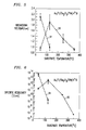
- the degradation of Ga2O3 film properties such as the dc breakdown field (Fig. 5) and specific resistivity (Fig. 6) at higher substrate temperatures may be attributed to oxygen loss during deposition.
- Fig. 5 is a plot of dc breakdown field vs. substrate temperature during deposition measured at 300 K for Ga2O3 films with thicknesses between 500 ⁇ and 4000 ⁇ , deposited with no excess oxygen at a background pressure of 1-2x10 ⁇ 6 Torr (Curve 51) and with 2x10 ⁇ 4 Torr oxygen present (Curve 52) in the evaporation chamber.
- the voltage at which destructive breakdown occurs, normalized to the film thickness, is defined as breakdown field E m .
- the breakdown voltage scales correctly with the oxide thickness for films thicker than 500 ⁇ . Slightly larger values for E m were obtained for thinner films.
- Fig. 6 shows a plot of specific resistivities vs. substrate temperature during deposition measured at 300 K for Ga2O3 films deposited at a background pressure of 1-2x10 ⁇ 6 Torr with no excess oxygen (Curve 61) and with 2x10 ⁇ 4 Torr oxygen present (Curve 62) in the evaporation chamber.
- the specific resistivity, p strongly depends on deposition conditions such as substrate temperature and oxygen partial pressure in the evaporation chamber during deposition, and is especially sensitive to substrate temperature for deposition with no excess oxygen.
- ⁇ (6 ⁇ 3) x 1013 ⁇ cm were again obtained for samples deposited at a substrate temperature of 40°C and a background pressure of 1-2x10 ⁇ 6 Torr with no excess oxygen during deposition.
- Fig. 7 is a plot of current vs. electric field characteristics of a Au/Ti/Ga2O3/GaAs metal/insulator/semiconductor structure measured at 300 K with an 864 ⁇ thick Ga2O3 film deposited at substrate temperature of 40°C and a background pressure of 1-2x10 ⁇ 6 Torr with no excess oxygen in the evaporation chamber.
- Two distinct regions of current transport, which is nearly independent of polarity of the electrodes, can be clearly identified.
- the Ohmic I-V characteristic at low fields is due to hopping of thermally excited electrons from one isolated state in the oxide to another. As illustrated in Fig.
- Capacitance measurements with no bias applied to the structure were done on said metal/insulator/metal (n+ Si substrate/TiW/Ga2O3/Ti/Au) structures with Ga2O3 films deposited at substrate temperature of 40°C and background pressure of 1-2x10 ⁇ 6 Torr with no excess oxygen in the evaporation chamber during deposition, and with Ga2O3 films deposited at substrate temperature of 125°C and an oxygen partial pressure of 2x10 ⁇ 4 Torr in the evaporation chamber during deposition.
- the capacitance is found to be independent on frequency within the measurement range between 100 Hz and 1 MHz, and scales correctly with oxide thickness.
Landscapes
- Chemical & Material Sciences (AREA)
- Chemical Kinetics & Catalysis (AREA)
- Engineering & Computer Science (AREA)
- Materials Engineering (AREA)
- Mechanical Engineering (AREA)
- Metallurgy (AREA)
- Organic Chemistry (AREA)
- Formation Of Insulating Films (AREA)
- Physical Deposition Of Substances That Are Components Of Semiconductor Devices (AREA)
- Physical Vapour Deposition (AREA)
- Semiconductor Lasers (AREA)
- Inorganic Insulating Materials (AREA)
Applications Claiming Priority (2)
| Application Number | Priority Date | Filing Date | Title |
|---|---|---|---|
| US08/217,296 US5451548A (en) | 1994-03-23 | 1994-03-23 | Electron beam deposition of gallium oxide thin films using a single high purity crystal source |
| US217296 | 1994-03-23 |
Publications (2)
| Publication Number | Publication Date |
|---|---|
| EP0674344A2 true EP0674344A2 (de) | 1995-09-27 |
| EP0674344A3 EP0674344A3 (de) | 1996-10-16 |
Family
ID=22810461
Family Applications (1)
| Application Number | Title | Priority Date | Filing Date |
|---|---|---|---|
| EP95301750A Withdrawn EP0674344A3 (de) | 1994-03-23 | 1995-03-16 | Dünne Schichten aus Gallium-Oxid. |
Country Status (6)
| Country | Link |
|---|---|
| US (1) | US5451548A (de) |
| EP (1) | EP0674344A3 (de) |
| JP (1) | JP3299657B2 (de) |
| KR (1) | KR950034587A (de) |
| CA (1) | CA2136581C (de) |
| TW (1) | TW266330B (de) |
Cited By (3)
| Publication number | Priority date | Publication date | Assignee | Title |
|---|---|---|---|---|
| WO1996005507A1 (de) * | 1994-08-09 | 1996-02-22 | Siemens Aktiengesellschaft | Verfahren zur herstellung eines gassensors |
| EP0863542A2 (de) * | 1997-03-04 | 1998-09-09 | Motorola, Inc. | Epitaxie eines III-V Wafers |
| US8518761B2 (en) | 2010-04-16 | 2013-08-27 | Semiconductor Energy Laboratory Co., Ltd. | Deposition method and method for manufacturing semiconductor device |
Families Citing this family (33)
| Publication number | Priority date | Publication date | Assignee | Title |
|---|---|---|---|---|
| US5962883A (en) * | 1994-03-23 | 1999-10-05 | Lucent Technologies Inc. | Article comprising an oxide layer on a GaAs-based semiconductor body |
| US5912498A (en) * | 1997-10-10 | 1999-06-15 | Lucent Technologies Inc. | Article comprising an oxide layer on GAN |
| US5550089A (en) * | 1994-03-23 | 1996-08-27 | Lucent Technologies Inc. | Gallium oxide coatings for optoelectronic devices using electron beam evaporation of a high purity single crystal Gd3 Ga5 O12 source. |
| US5597768A (en) * | 1996-03-21 | 1997-01-28 | Motorola, Inc. | Method of forming a Ga2 O3 dielectric layer |
| US5665658A (en) * | 1996-03-21 | 1997-09-09 | Motorola | Method of forming a dielectric layer structure |
| US5903037A (en) * | 1997-02-24 | 1999-05-11 | Lucent Technologies Inc. | GaAs-based MOSFET, and method of making same |
| US5904553A (en) * | 1997-08-25 | 1999-05-18 | Motorola, Inc. | Fabrication method for a gate quality oxide-compound semiconductor structure |
| US6025281A (en) * | 1997-12-18 | 2000-02-15 | Motorola, Inc. | Passivation of oxide-compound semiconductor interfaces |
| US5945718A (en) * | 1998-02-12 | 1999-08-31 | Motorola Inc. | Self-aligned metal-oxide-compound semiconductor device and method of fabrication |
| US6159834A (en) * | 1998-02-12 | 2000-12-12 | Motorola, Inc. | Method of forming a gate quality oxide-compound semiconductor structure |
| US6094295A (en) * | 1998-02-12 | 2000-07-25 | Motorola, Inc. | Ultraviolet transmitting oxide with metallic oxide phase and method of fabrication |
| US6495407B1 (en) | 1998-09-18 | 2002-12-17 | Agere Systems Inc. | Method of making an article comprising an oxide layer on a GaAs-based semiconductor body |
| SG85604A1 (en) * | 1998-11-06 | 2002-01-15 | Inst Materials Research & Eng | Method of selective post-growth tuning of an optical bandgap of a semi-conductor heterostructure and products produced thereof |
| US6521961B1 (en) | 2000-04-28 | 2003-02-18 | Motorola, Inc. | Semiconductor device using a barrier layer between the gate electrode and substrate and method therefor |
| US6670651B1 (en) | 2000-05-04 | 2003-12-30 | Osemi, Inc. | Metal sulfide-oxide semiconductor transistor devices |
| US6936900B1 (en) | 2000-05-04 | 2005-08-30 | Osemi, Inc. | Integrated transistor devices |
| US6451711B1 (en) * | 2000-05-04 | 2002-09-17 | Osemi, Incorporated | Epitaxial wafer apparatus |
| US6445015B1 (en) | 2000-05-04 | 2002-09-03 | Osemi, Incorporated | Metal sulfide semiconductor transistor devices |
| US7442654B2 (en) * | 2002-01-18 | 2008-10-28 | Freescale Semiconductor, Inc. | Method of forming an oxide layer on a compound semiconductor structure |
| US6933244B2 (en) * | 2002-01-22 | 2005-08-23 | Massachusetts Institute Of Technology | Method of fabrication for III-V semiconductor surface passivation |
| ATE393839T1 (de) * | 2002-04-15 | 2008-05-15 | Schott Ag | Verfahren zur gehäusebildung bei elektronischen bauteilen so wie so hermetisch verkapselte elektronische bauteile |
| US6989556B2 (en) * | 2002-06-06 | 2006-01-24 | Osemi, Inc. | Metal oxide compound semiconductor integrated transistor devices with a gate insulator structure |
| US7187045B2 (en) * | 2002-07-16 | 2007-03-06 | Osemi, Inc. | Junction field effect metal oxide compound semiconductor integrated transistor devices |
| JP3763021B2 (ja) * | 2003-05-26 | 2006-04-05 | 学校法人関西学院 | 電子ビーム微細加工方法 |
| WO2005048318A2 (en) * | 2003-11-17 | 2005-05-26 | Osemi, Inc. | Nitride metal oxide semiconductor integrated transistor devices |
| US20080282983A1 (en) * | 2003-12-09 | 2008-11-20 | Braddock Iv Walter David | High Temperature Vacuum Evaporation Apparatus |
| US7223441B2 (en) * | 2004-03-10 | 2007-05-29 | Pilkington North America, Inc. | Method for depositing gallium oxide coatings on flat glass |
| JP2007134445A (ja) * | 2005-11-09 | 2007-05-31 | Nichia Chem Ind Ltd | 窒化物半導体レーザ素子 |
| US7483212B2 (en) * | 2006-10-11 | 2009-01-27 | Rensselaer Polytechnic Institute | Optical thin film, semiconductor light emitting device having the same and methods of fabricating the same |
| JP3950473B2 (ja) * | 2006-11-06 | 2007-08-01 | シャープ株式会社 | 化合物半導体レーザ |
| US20080157073A1 (en) * | 2006-12-29 | 2008-07-03 | Walter David Braddock | Integrated Transistor Devices |
| DE102008020793A1 (de) | 2008-04-22 | 2009-11-05 | Forschungsverbund Berlin E.V. | Halbleiterbauelement, Vorprodukt und Verfahren zur Herstellung |
| WO2011158704A1 (en) * | 2010-06-18 | 2011-12-22 | Semiconductor Energy Laboratory Co., Ltd. | Method for manufacturing semiconductor device |
Family Cites Families (4)
| Publication number | Priority date | Publication date | Assignee | Title |
|---|---|---|---|---|
| CA920285A (en) * | 1970-11-30 | 1973-01-30 | L. Hartman Robert | Extending the operating life of light emitting p-n junction devices |
| US4617192A (en) * | 1982-12-21 | 1986-10-14 | At&T Bell Laboratories | Process for making optical INP devices |
| US4749255A (en) * | 1985-12-09 | 1988-06-07 | American Telephone And Telegraph Company, At&T Bell Laboratories | Coating for optical devices |
| DE4321301A1 (de) * | 1992-07-06 | 1994-01-13 | Zeiss Carl Fa | Dünne Schicht aus Galliumoxid und Herstellverfahren dafür |
-
1994
- 1994-03-23 US US08/217,296 patent/US5451548A/en not_active Expired - Lifetime
- 1994-11-22 TW TW083110877A patent/TW266330B/zh not_active IP Right Cessation
- 1994-11-24 CA CA002136581A patent/CA2136581C/en not_active Expired - Fee Related
-
1995
- 1995-03-10 KR KR1019950004863A patent/KR950034587A/ko not_active Withdrawn
- 1995-03-16 EP EP95301750A patent/EP0674344A3/de not_active Withdrawn
- 1995-03-23 JP JP06371295A patent/JP3299657B2/ja not_active Expired - Lifetime
Cited By (6)
| Publication number | Priority date | Publication date | Assignee | Title |
|---|---|---|---|---|
| WO1996005507A1 (de) * | 1994-08-09 | 1996-02-22 | Siemens Aktiengesellschaft | Verfahren zur herstellung eines gassensors |
| EP0863542A2 (de) * | 1997-03-04 | 1998-09-09 | Motorola, Inc. | Epitaxie eines III-V Wafers |
| US8518761B2 (en) | 2010-04-16 | 2013-08-27 | Semiconductor Energy Laboratory Co., Ltd. | Deposition method and method for manufacturing semiconductor device |
| US9006046B2 (en) | 2010-04-16 | 2015-04-14 | Semiconductor Energy Laboratory Co., Ltd. | Deposition method and method for manufacturing semiconductor device |
| US9698008B2 (en) | 2010-04-16 | 2017-07-04 | Semiconductor Energy Laboratory Co., Ltd. | Deposition method and method for manufacturing semiconductor device |
| US10529556B2 (en) | 2010-04-16 | 2020-01-07 | Semiconductor Energy Laboratory Co., Ltd. | Deposition method and method for manufacturing semiconductor device |
Also Published As
| Publication number | Publication date |
|---|---|
| US5451548A (en) | 1995-09-19 |
| CA2136581C (en) | 1998-08-04 |
| EP0674344A3 (de) | 1996-10-16 |
| JPH07268609A (ja) | 1995-10-17 |
| JP3299657B2 (ja) | 2002-07-08 |
| KR950034587A (ko) | 1995-12-28 |
| TW266330B (de) | 1995-12-21 |
| CA2136581A1 (en) | 1995-09-24 |
Similar Documents
| Publication | Publication Date | Title |
|---|---|---|
| US5451548A (en) | Electron beam deposition of gallium oxide thin films using a single high purity crystal source | |
| Passlack et al. | Dielectric properties of electron‐beam deposited Ga2O3 films | |
| Sclar | Properties of rare‐earth nitrides | |
| Maissel et al. | An introduction to thin films | |
| US4416952A (en) | Oxynitride film and its manufacturing method | |
| Rand et al. | Preparation and properties of thin film boron nitride | |
| Heiland et al. | Polar surfaces of zinc oxide crystals | |
| US4859253A (en) | Method for passivating a compound semiconductor surface and device having improved semiconductor-insulator interface | |
| Yan et al. | Structural and electrical characterization of TiO2 grown from titanium tetrakis‐isopropoxide (TTIP) and TTIP/H2O ambients | |
| Green et al. | Nucleation and growth of atomic layer deposited HfO 2 gate dielectric layers on chemical oxide (Si–O–H) and thermal oxide (SiO 2 or Si–O–N) underlayers | |
| Dong et al. | Preparation and Some Properties of Chemically Vapor‐Deposited Si‐Rich SiO2 and Si3 N 4 Films | |
| US6404027B1 (en) | High dielectric constant gate oxides for silicon-based devices | |
| EP0674017B1 (de) | Galliumoxid-Beschichtung für optoelektronische Bauelemente | |
| Hu et al. | Silicon nitride films by reactive sputtering | |
| Bath et al. | Plasma enhanced chemical vapor deposition and characterization of boron nitride gate insulators on InP | |
| CA1209949A (en) | Method of producing articles by vapor deposition of multiconstituent material | |
| Melliar‐Smith et al. | Chemically vapor deposited tungsten for semiconductor metallizations | |
| Chesler et al. | dc plasma anodization of GaAs | |
| Hall et al. | Properties of aluminum oxide films obtained from nitrous oxide and aluminum trimethyl | |
| Alonso et al. | Low temperature sio2 films deposited by plasma enhanced techniques | |
| Bhat et al. | Reactive ion beam deposition of aluminum nitride thin films | |
| Bose et al. | Electrical conduction studies of plasma enhanced chemical vapor deposited silicon nitride films | |
| Šmíd et al. | Field effect in dc-sputtered a-Si: H in structure using SiNx prepared in situ | |
| Kozuma et al. | Some Properties of Silica Film Made by RF Glow Discharge Sputtering | |
| Santinelli et al. | Ion beam enhanced deposition of AINxOy alloys on InP |
Legal Events
| Date | Code | Title | Description |
|---|---|---|---|
| PUAI | Public reference made under article 153(3) epc to a published international application that has entered the european phase |
Free format text: ORIGINAL CODE: 0009012 |
|
| AK | Designated contracting states |
Kind code of ref document: A2 Designated state(s): DE FR GB |
|
| PUAL | Search report despatched |
Free format text: ORIGINAL CODE: 0009013 |
|
| AK | Designated contracting states |
Kind code of ref document: A3 Designated state(s): DE FR GB |
|
| 17P | Request for examination filed |
Effective date: 19970403 |
|
| 17Q | First examination report despatched |
Effective date: 19980519 |
|
| STAA | Information on the status of an ep patent application or granted ep patent |
Free format text: STATUS: THE APPLICATION IS DEEMED TO BE WITHDRAWN |
|
| 18D | Application deemed to be withdrawn |
Effective date: 19980930 |