EP0675436B1 - Antémémoire associative récupérable - Google Patents
Antémémoire associative récupérable Download PDFInfo
- Publication number
- EP0675436B1 EP0675436B1 EP94309056A EP94309056A EP0675436B1 EP 0675436 B1 EP0675436 B1 EP 0675436B1 EP 94309056 A EP94309056 A EP 94309056A EP 94309056 A EP94309056 A EP 94309056A EP 0675436 B1 EP0675436 B1 EP 0675436B1
- Authority
- EP
- European Patent Office
- Prior art keywords
- data
- line
- replacement
- address
- faulty
- Prior art date
- Legal status (The legal status is an assumption and is not a legal conclusion. Google has not performed a legal analysis and makes no representation as to the accuracy of the status listed.)
- Expired - Lifetime
Links
Images

Classifications
-
- G—PHYSICS
- G11—INFORMATION STORAGE
- G11C—STATIC STORES
- G11C29/00—Checking stores for correct operation ; Subsequent repair; Testing stores during standby or offline operation
- G11C29/70—Masking faults in memories by using spares or by reconfiguring
- G11C29/88—Masking faults in memories by using spares or by reconfiguring with partially good memories
-
- G—PHYSICS
- G06—COMPUTING OR CALCULATING; COUNTING
- G06F—ELECTRIC DIGITAL DATA PROCESSING
- G06F12/00—Accessing, addressing or allocating within memory systems or architectures
- G06F12/02—Addressing or allocation; Relocation
- G06F12/08—Addressing or allocation; Relocation in hierarchically structured memory systems, e.g. virtual memory systems
- G06F12/12—Replacement control
- G06F12/121—Replacement control using replacement algorithms
- G06F12/126—Replacement control using replacement algorithms with special data handling, e.g. priority of data or instructions, handling errors or pinning
-
- G—PHYSICS
- G06—COMPUTING OR CALCULATING; COUNTING
- G06F—ELECTRIC DIGITAL DATA PROCESSING
- G06F2212/00—Indexing scheme relating to accessing, addressing or allocation within memory systems or architectures
- G06F2212/10—Providing a specific technical effect
- G06F2212/1032—Reliability improvement, data loss prevention, degraded operation etc
Definitions
- the present invention relates generally to integrated circuit memories, and more specifically to set associative cache memories.
- die are often discarded when certain bits of the die are defective but not easily identified and repaired. Even though a majority of the die may be fully functional, it is often necessary to discard the entire die if the faulty bits of the die are not repairable. This problem is exacerbated when a memory device is embedded in another, more expensive device such as a microprocessor or an application specific integrated circuit (ASIC). For example, it is undesirable to discard a costly microprocessor because the memory embedded within it has faulty bits.
- Memories which may have faulty bits include cache memories, memory cards, and memories embedded in ASICs.
- Cache memories are important elements of the typical cache system and are increasingly used as primary caches embedded in high performance microprocessors or as secondary caches external to the microprocessor. As microprocessors have achieved faster operating speed, the rate at which requested data must be supplied to them has correspondingly increased. Cache memories typically have faster access times than main memory and thus are often used to quickly supply data requested by the microprocessor.
- the tag associated with a "line" of data a block of data which can be one or several consecutive bytes or words of data, in the cache memory is stored in a tag RAM which holds the address locations of data stored in the data cache.
- one or more status bits often including a valid bit which indicates whether data stored at a particular address location is valid or invalid, is stored in the tag RAM.
- a read signal is sent to both the main memory and the tag RAM.
- the tag RAM compares the requested memory address with the memory address of all data stored in the cache memory. If the requested memory address is in the tag RAM, a "hit" condition exists, and data from that location will be gated from the cache memory to the microprocessor.
- the tag RAM In a "hit” condition, the tag RAM generates a valid compare Match output signal and the cache memory gates the required data onto the data bus before the main memory can respond. In this way, the cache memory quickly supplies data to the microprocessor and microprocessor wait states are avoided.
- the tag RAM's comparison operation indicates that the desired data is not stored inside the cache memory, a "miss” condition exists, and the data must come from main memory which typically holds more data than the cache memory and is therefore much slower.
- the microprocessor may have to wait for several cycles, during which time it is idle, before receiving requested data from main memory. These unproductive cycles are referred to as "wait states" since the microprocessor must wait until the requested data is provided from main memory.
- set-associative cache memories are often used because of the performance enhancement they can provide.
- a set-associative cache memory there are two or more "sets" from which data may be supplied to the microprocessor. Thus, if one set does not contain the requested data, another set may very well be able to provide valid data.
- the cache is split into two smaller, somewhat independent caches. This allows for two tags to be stored for a given index address and the two associated lines of data in each cache memory; the index of the tag is the least significant bits (LSBs) of the address field, used to address a given tag location, and the tag bits are the least significant bits (MSBs).
- LSBs least significant bits
- MSBs least significant bits
- FIG. 1 shows a block diagram of a set-associative cache system 10 which is comprised of five main elements: microprocessor 12, main memory 13, tag RAM A 14, tag RAM B 16, cache memory set A 18, cache memory set B 19, and control logic 20. Because the cache memory is separate from the microprocessor, cache system 10 is a secondary cache system which is shown for clarity. In a primary cache system, cache memory set A 18 and set B 19 would be embedded in the microprocessor, and thus is sometimes called an embedded cache memory. Microprocessor 12 could obtain all needed data from the slow main memory 13. However, since main memory 13 is typically much slower than microprocessor 12, microprocessor 12 will incur “wait states" until the data arrives from main memory 13. During wait states, microprocessor 12 is idle. Wait states have a negative impact on the efficiency of the microprocessor.
- a cache system is used to provide the microprocessor with data in a more timely fashion, in the hopes of reducing or even eliminating microprocessor wait states.
- the secondary cache system composed of tag RAM A 14, tag RAM B 16, cache memory set A 18, cache memory set B 19, and control logic 20, resides between microprocessor 12 and main memory 13.
- Set A 18 and set B 19 together comprise a two-way set associative cache memory and each store a copy of frequently accessed main memory data. Storing data commonly accessed by the microprocessor 12 increases the likelihood that cache memory set A 18 or set B 19 will have the requested data in the event of a microprocessor memory cycle.
- cache memory set A 18 or cache memory set B 19 will supply data to microprocessor 12 upon a microprocessor read cycle if they have the requested data.
- Tag RAM A 14 determines if cache memory set A 18 has the data requested by the microprocessor 12 while tag RAM B 16 determines if cache memory set B 19 has the requested data;
- Tag RAM A 14 stores the memory addresses and status bit information of data stored in cache memory set A 18 and
- tag RAM B 16 stores the memory addresses and status bit information of data stored in cache memory set B 19.
- Valid bit 17 is a status bit which indicates whether the data stored at a particular address location is valid or invalid.
- Valid bit 17 is tied to a logic high voltage level, V CC , as shown in Figure 1, such that subsequent write cycles from microprocessor 12 write a "one" to newly written tag RAM address locations. Until microprocessor 12 writes data to a cache memory location, the valid bit 17 for that address location will be invalid or equal to a logic low level.
- the tag RAM A 14 and tag RAM B 16 compare the address of the data being sought with the addresses of data stored in the cache memory set A 18 and cache memory set B 19, respectively. If a "hit" or match condition exists in either set A 18 or set B 19 and the valid bit 17 as well as other status bits for that address index location are valid, the appropriate tag RAM A 14 or tag RAM B 16 generates a logic high Match output signal 15 which indicates that its cache memory set A 18 or set B 19 has the desired data. Control logic 20 determines which set will provide the data as a function of the match and status bits, and data from the appropriate set of the cache memory is then gated onto the data bus where it is received by microprocessor 12.
- tag RAM A 14 or tag RAM B16 determines the desired data address does not match any addresses stored in the cache memory set A 18 or cache memory set B 19, respectively. Or, if the desired data address matches an address stored in cache memory set A 18 or cache memory set B 19 but valid bit 17 for that address is invalid, a "miss” condition also exists. In response to a "miss” condition, the tag RAM generates a logic low Match output signal.
- Match output signal 15 functions as a high-speed chip select which allows or does not allow data from the cache memory to be gated onto the data bus to the microprocessor. If the tag RAM comparison function indicates a "hit” condition then the cache memory outputs are simply enabled. If a "miss” condition is indicated, the outputs of the appropriate cache memory set are not enabled and main memory 13 will ultimately supply the data to the microprocessor 12.
- replacement algorithms such as the least recently used (LRU), the first in first out (FIFO), the last in first out (LIFO), the random replacement algorithm, and the pseudo LRU replacement algorithm are used to determine whether a replacement line of data from main memory will be used to update set A 18 or set B 19.
- LRU least recently used
- FIFO first in first out
- LIFO last in first out
- random replacement algorithm and the pseudo LRU replacement algorithm are used to determine whether a replacement line of data from main memory will be used to update set A 18 or set B 19.
- a set associative cache memory where one or more sets have randomly occurring bit(s) failures is often discarded.
- set associative cache memories may suffer from bit failures due to randomly occurring process problems such as single bit failures, particle contamination, locked rows, locked columns, and metal or polysilicon shorts. These failures may not be easily repaired, especially if no row or column redundancy testing is employed. Even when redundancy testing at laser repair is used, this technique may not be sufficient to ferret out all bit failures. Therefore, when a set associative cache memory having bit(s) failures is resident in microprocessors, ASICs, or other devices, both the faulty cache memory and the expensive fully functional device in which it is embedded are often discarded.
- a method of bypassing a faulty line of.data or its associated tag of a set associative cache memory comprising the steps of identifying an address of a faulty line of data associated with a first set of a set associative cache memory, characterised by generating a faulty line of data address signal corresponding to the address of the faulty line of data, performing logic on the faulty line of data address signal, an address hit/miss signal and a status bit signal to produce a logic state of a replacement status bit of the faulty line of data that flags the address of the faulty line of data, wherein the address hit/miss signal indicates whether there is a cache hit or a cache miss condition for the first set associative cache memory, flagging the address of the faulty line of data using a replacement logic circuit so that when a replacement line of data having an address corresponding to the address of the faulty line of data is to be written to the set associative cache memory, the replacement line of data is written to a second set of the set
- the present invention also provides a structure for bypassing a faulty line of data or its associated tag of a set associative cache memory, comprising a set associative cache memory having a plurality of lines of data contained in a plurality of sets with each line of data having at least one replacement status bit associated with it which indicates when each line of data was used relative to other lines of data of different sets corresponding to an address characterised by a faulty address indentification block which identifies an address of a faulty line of data of the plurality of lines of data of a set of the plurality of sets, a logic element having the address of the faulty line of data as an input signal which generates a faulty line of data address signal corresponding to the address of the faulty line of data, a replacement logic circuit which performs logic on the faulty line of data address signal, an address hit/miss signal and a status bit signal to produce a logic state of a replacement status bit of the faulty line of data that flags the address of the faulty line of data such that when an address of
- Set-associative cache memories are attractive because of the higher hit rate and performance advantages they offer over conventional direct-mapped cache memories. Because set associative cache memories are comprised of two or more sets of data, the control circuitry that determines which set to update following a cache miss condition is complex. In order to keep track of which set of data to update following a cache miss condition, replacement logic algorithms such as the Least Recently Used (LRU), the First In First Out (FIFO), the Last In First Out (LIFO), the random replacement algorithm, and the pseudo LRU replacement algorithm are typically used.
- LRU Least Recently Used
- FIFO First In First Out
- LIFO Last In First Out
- random replacement algorithm the pseudo LRU replacement algorithm
- the present invention utilizes replacement logic circuitry that controls the set selection of a set associative cache memory in order to ensure that faulty lines of data of a set are not updated and effectively bypassed following a cache miss condition; a bad line of data within a set is not selected to be updated.
- a faulty line of data is defined as a line of data which contains one or more faulty bits of data.
- the faulty bits of data exist in the set associative cache memory in the data cache (or its associated tag), which stores various lines of data. Updating refers to writing to a particular location of the set associative cache memory with a new line of data.
- Individual faulty data locations of a set are communicated to the replacement logic circuitry so that during set selection of the set associative cache memory, a set containing a faulty line of data for a particular index address is never selected and hence effectively bypassed.
- the present invention may be utilized after traditional redundancy testing has or has not been performed.
- the present invention may be used in a variety of cache applications which use set-associative cache memories and is especially advantageous when used to render large cache memories usable rather than discarding them; the present invention allows large cache memories to be used since yield limitations are reduced. Also, valuable devices such as microprocessors and ASICs which utilize embedded set associative cache memory may be salvaged.
- the present invention may be used to render embedded memory having defects such as single bits, locked rows, locked columns, particle contamination, and the like, usable.
- LRU replacement algorithm for example, then the least recently used line of data of the set-associative cache is chosen to be replaced, and all the status bits for the requested index address are updated to reflect the new LRU status for the associated tags.
- a two-way set associative cache would require only a one bit replacement status bit per tag since there are only two sets in which data is stored; similarly, for a four-way set associative cache memory two replacement status bits are required per tag since there are four sets in which data is stored.
- a first logic level, for instance a logic low level, on the replacement status bit would indicate that a line of data is the LRU line of data
- a second logic level, such as a logic high level, on the replacement status bit would indicate that the line of data is a more recently used line of data contained in the tag for that index address.
- a more recently used line of data may or may not be the most recently used (MRU) line of data. For instance, in a two-way set associative cache the more recently used line of data is the MRU line of data, whereas in a larger set associative cache memory such as a four-way set associative cache, a more recently used line of data need not be the MRU line of data.
- the replacement status bit of a replacement line of data from main memory would be set to a high logic level, and the replacement status bit of the remaining line of data in the other set which was not replaced would be reset to a low logic level since it is now the LRU line of data for the index address.
- cache memory set A 32 of a two-way set associative cache memory contains a faulty line of data 34 containing one or more faulty bits of data.
- the replacement status bit of the index address associated with the faulty line of data 34 of set A 32 is always forced to a logic high level, and the replacement status bit associated with line of data 38 of cache memory set B 36 is always forced to a logic low level, for this two-way set associative cache memory LRU example.
- a replacement line of data 42 from main memory 40 would always replace the line of data 38 of cache memory set B 36 and would never update the faulty line of data 34 of cache memory set A 32 which is effectively bypassed.
- the faulty line of data 34 is identified by programming means which are communicated to replacement logic circuitry.
- the programming means may be accomplished using a variety of fuse programming or storage in registers techniques well known in the art. For instance, registers may be loaded using a Built-In Self Test (BIST) circuit. Additionally, nonvolatile programming means such as electrically programmable read only memories (EPROMs), electrically erasable programmable read only memories (EEPROMs), Flash EPROMs, etc. may be used.
- EPROMs electrically programmable read only memories
- EEPROMs electrically erasable programmable read only memories
- Flash EPROMs etc.
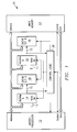
- circuitry 50 having replacement logic circuit 60 is shown.
- Replacement logic circuit 60 has been divided into four segments, marked by dashed lines as shown, to represent set A, set B, set C, and set D of a four-way set associative cache memory.
- the input signals 59, 62, and 64 shown are for set A only and thus the circuitry 52-58, input signals 62, 64, and output signal 66 would be duplicated for each set.
- Replacement logic circuit 60 will perform logic on four signals analogous to signals 59, 62, and 64 in order to produce signal 66.
- a plurality of faulty addresses of a faulty line of data are identified using faulty address identification blocks 52, 54, and 56, which, as mentioned, may contain fuse circuitry or register circuitry well known in the art.
- the output signals of faulty address identification blocks 52, 54, and 56 are input signals to logic circuitry, such as logic OR gate 58, which produces signal 59.
- Signal 59, address hit/miss signal 62, and status bit(s) signal 64 are all input signals to replacement logic circuit 60 as shown and these signals are associated with a particular set, set A.
- Address hit/miss signal 62 indicates whether there is a cache hit or a cache miss condition for set A
- status bits signal 64 provides status information concerning set A including the logic level of a replacement status bit of set A to replacement logic circuit 60.
- Replacement logic circuit 60 performs logic on signals 59, 62, and 64 to produce signal 66 which determines the replacement status bit definition.
- replacement logic circuit 60 may be used in conjunction with a first preferred embodiment which uses a LRU replacement algorithm.
- Replacement logic circuit 60 may also be used in conjunction with a second preferred embodiment which also uses a LRU replacement algorithm, as an example.
- a set containing a faulty line of data would not be bypassed by forcing its replacement status bit to a predetermined logic level. Rather, when the faulty line of data becomes the LRU line of data, it is not updated based on the programming means. discussed earlier.
- the programming means define the faulty line of data as faulty so that it is not updated. Instead, the line of data to be updated next, for instance the LRU + 1 line of data, will be immediately updated.
- the replacement logic circuitry will detect the states of each of the four replacement status bits associated with each of the four sets.
- the replacement status bit for any faulty line of data will cause the faulty line of data to not be updated following a cache miss condition.
- a cache miss Upon a cache miss, a new line of data is brought into the cache from main memory. An existing line of data must be replaced by the incoming replacement line, assuming the cache is full.
- the choice of which line of data to replace is based on the state of the replacement status bits in the tag of the index address associated with each line of data stored in the cache. Thus, the faulty location is fixed such that it is not chosen for replacement.
- the two-way set associative cache LRU example described herein is but one embodiment of the present invention.
- the present invention is equally well suited for use with other replacement algorithms previously mentioned, such as the FIFO replacement algorithm, the LIFO replacement algorithm, the random replacement algorithm, and the pseudo LRU replacement algorithm.
Landscapes
- Engineering & Computer Science (AREA)
- Theoretical Computer Science (AREA)
- Physics & Mathematics (AREA)
- General Engineering & Computer Science (AREA)
- General Physics & Mathematics (AREA)
- Memory System Of A Hierarchy Structure (AREA)
- For Increasing The Reliability Of Semiconductor Memories (AREA)
Claims (25)
- Procédé de contournement d'une ligne défectueuse de données ou de son étiquette associée d'une antémémoire associative, comprenant les étapes suivantes :l'identification d'une adresse d'une ligne de données défectueuse associée à un premier banc d'une antémémoire associative, caractérisée par :la production d'un signal d'adresse de ligne de données défectueuse (59) correspondant à l'adresse de la ligne de données défectueuse ;la réalisation d'opérations logiques sur le signal d'adresse de ligne de données défectueuse (59), sur un signal de présence/absence d'adresse (62) et sur un signal de bit d'état (64) pour produire un état logique d'un bit d'état de remplacement de la ligne de données défectueuse qui marque l'adresse de la ligne de données défectueuse, dans lequel le signal de présence/absence d'adresse (62) indique s'il y a une condition de présence dans l'antémémoire ou d'absence dans l'antémémoire pour le premier banc de l'antémémoire associative ;le marquage de l'adresse de la ligne de données défectueuse en utilisant un circuit logique de remplacement (60) de sorte que lorsqu'une ligne de remplacement de données ayant une adresse correspondant à l'adresse de la ligne défectueuse de données est à écrire dans l'antémémoire associative, la ligne de remplacement de données est écrite dans un second banc de l'antémémoire associative, comme le détermine le circuit logique de remplacement, contournant, de manière efficace, la ligne de données défectueuse du premier banc.
- Procédé selon la revendication 1, dans lequel l'antémémoire associative possède une pluraiité de lignes de données contenues dans une pluralité de bancs et chaque ligne de données a une adresse et au moins un bit d'état de remplacement associé à cette dernière qui indique quand chaque ligne de données est utilisée par rapport aux autres lignes de données de bancs différents correspondant à la même adresse.
- Procédé selon la revendication 2, dans lequel le circuit logique de remplacement utilise un algorithme de remplacement à l'ancienneté (LRU) pour mettre à jour une ligne de données la plus ancienne (LRU) par la ligne de données de remplacement.
- Procédé selon la revendication 3, dans lequel le bit d'état de remplacement de la ligne de données défectueuse est forcé à un premier niveau logique qui désigne la ligne défectueuse de données comme une ligne de données la plus récente qui n'est pas mise à jour par la ligne de données de remplacement, plutôt qu'une ligne de données du second banc dont le bit d'état de remplacement est égal à un second niveau logique qui désigne la ligne de données en tant que ligne de données la plus ancienne (LRU) qui est mise à jour par la ligne de données de remplacement.
- Procédé selon la revendication 3, dans lequel, lorsque le bit d'état de remplacement d'une ligne de données désigne la ligne de données en tant que ligne de données la plus ancienne (LRU), la ligne de données est mise à jour par la ligne de données de remplacement ; cependant, lorsque la ligne de données défectueuse est la ligne de données LRU, la ligne de données défectueuse est contournée et une autre ligne de données est mise à jour par la ligne de données de remplacement comme le détermine le circuit logique de remplacement.
- Procédé selon la revendication 1, dans lequel des moyens de programmation sont utilisés pour identifier l'adresse de la ligne de données défectueuse.
- Procédé selon la revendication 6, dans lequel les moyens de programmation utilisent une programmation par fusible.
- Procédé selon la revendication 6, dans lequel les moyens de programmation utilisent une pluralité de registres.
- Procédé selon la revendication 8, dans lequel les registres sont chargés en utilisant un circuit à autocontrôle intégré (BIST).
- Procédé selon la revendication 6, dans lequel les moyens de programmation utilisent des dispositifs non volatils.
- Procédé selon la revendication 1, dans lequel le circuit logique de remplacement utilise l'un ou l'autre d'un premier algorithme de remplacement premier entré premier sorti (FIFO) ; ou d'un algorithme de remplacement dernier entré premier sorti (LIFO) ; ou d'un algorithme de remplacement aléatoire ; ou d'un algorithme de remplacement fictif à l'ancienneté (LRU).
- Procédé selon la revendication 11, dans lequel l'antémémoire associative est une antémémoire intégrée.
- Procédé selon la revendication 12, dans lequel l'antémémoire intégrée est une antémémoire primaire d'un microprocesseur.
- Structure pour contourner une ligne de données défectueuse ou son étiquette associé d'une antémémoire associative, comprenant :une antémémoire associative ayant une pluralité de lignes de données contenues dans une pluralité de bancs, chaque ligne de données ayant au moins un bit d'état de remplacement associé à cette dernière qui indique quand chaque ligne de données est utilisée par rapport aux autres lignes de données de bancs différents correspondant à une adresse, caractérisée par :un bloc d'identification d'adresse défectueuse (52, 54, 56) qui identifie une adresse d'une ligne de données défectueuse de la pluralité de lignes de données d'un banc de ia pluralité de bancs ;un élément logique (58) ayant l'adresse de la ligne de données défectueuse en tant que signal d'entrée qui produit un signal d'adresse de ligne de données défectueuse (59) correspondant à l'adresse de la ligne de données défectueuse ;un circuit logique de remplacement (60) qui effectue des opérations logiques sur le signal d'adresse de ligne de données défectueuse (59), sur un signal de présence/absence d'adresse (62) et sur un signal de bit d'état (64) pour produire un état logique d'un bit d'état de remplacement de la ligne de données défectueuse qui marque l'adresse de la ligne de données défectueuse de sorte que lorsqu'une adresse d'une ligne de données défectueuse est détectée pendant un cycle de remplacement suivant une condition d'absence dans l'antémémoire, la ligne de données défectueuse est contournée, dans lequel le signal de présence/absence d'adresse indique s'il y a une condition de présence dans l'antémémoire ou d'absence dans l'antémémoire pour le premier banc de l'antémémoire associative.
- Structure selon la revendication 14, dans laquelle le circuit logique de remplacement utilise un algorithme de remplacement à l'ancienneté (LRU) pour mettre à jour une ligne de données la plus ancienne (LRU) par une ligne de données de remplacement.
- Structure selon la revendication 14, dans laquelle le bit d'état de remplacement de la ligne de données défectueuse est forcé à un premier niveau logique qui désigne la ligne de données défectueuse comme une ligne de données la plus récente qui n'est pas mise à jour par la ligne de données de remplacement, alors qu'une ligne de données dont le bit d'état de remplacement est égal à un second niveau logique qui désigne la ligne de données en tant que ligne de données la plus ancienne (LRU) qui est mise à jour par la ligne de données de remplacement.
- Structure selon la revendication 16, dans laquelle, lorsque le bit d'état de remplacement d'une ligne de données désigne la ligne de données en tant que ligne de données la plus ancienne (LRU), la ligne de données est mise à jour par la ligne de données de remplacement ; cependant, lorsque la ligne de données défectueuse est la ligne de données LRU, la ligne de données défectueuse est contournée et une autre ligne de données est mise à jour avec la ligne de données de remplacement comme le détermine le circuit logique de remplacement.
- Structure selon la revendication 14, dans laquelle des moyens de programmation sont utilisés pour identifier l'adresse de la ligne de données défectueuse.
- Structure selon la revendication 18, dans laquelle les moyens de programmation utilisent une programmation par fusible.
- Structure selon la revendication 18, dans laquelle les moyens de programmation utilisent une pluralité de registres.
- Structure selon la revendication 20, dans laquelle les registres sont chargés en utilisant un circuit à autocontrôle intégré (BIST).
- Structure selon la revendication 18, dans laquelle les moyens de programmation utilisent des dispositifs non volatils.
- Structure selon la revendication 14, dans laquelle le circuit logique de remplacement utilise l'un ou l'autre d'un premier algorithme de remplacement premier entré premier sorti (FIFO) ; ou d'un algorithme de remplacement dernier entré premier sorti (LIFO) ; ou d'un algorithme de remplacement aléatoire ; ou d'un algorithme de remplacement fictif à l'ancienneté (LRU).
- Structure selon la revendication 14, dans laquelle l'antémémoire associative est une antémémoire intégrée.
- Structure selon la revendication 24, dans lequel l'antémémoire intégrée est une antémémoire primaire d'un microprocesseur.
Applications Claiming Priority (2)
| Application Number | Priority Date | Filing Date | Title |
|---|---|---|---|
| US22107294A | 1994-03-31 | 1994-03-31 | |
| US221072 | 1994-03-31 |
Publications (2)
| Publication Number | Publication Date |
|---|---|
| EP0675436A1 EP0675436A1 (fr) | 1995-10-04 |
| EP0675436B1 true EP0675436B1 (fr) | 1999-10-27 |
Family
ID=22826220
Family Applications (1)
| Application Number | Title | Priority Date | Filing Date |
|---|---|---|---|
| EP94309056A Expired - Lifetime EP0675436B1 (fr) | 1994-03-31 | 1994-12-06 | Antémémoire associative récupérable |
Country Status (4)
| Country | Link |
|---|---|
| US (1) | US5666482A (fr) |
| EP (1) | EP0675436B1 (fr) |
| JP (1) | JPH0822417A (fr) |
| DE (1) | DE69421379T2 (fr) |
Families Citing this family (38)
| Publication number | Priority date | Publication date | Assignee | Title |
|---|---|---|---|---|
| US6044441A (en) * | 1995-09-29 | 2000-03-28 | Intel Corporation | Method and apparatus for encoding valid and invalid states in a cache with an invalid pattern |
| JPH09319569A (ja) * | 1996-05-31 | 1997-12-12 | Mitsubishi Electric Corp | マイクロコンピュータ |
| US6412051B1 (en) * | 1996-11-27 | 2002-06-25 | International Business Machines Corp. | System and method for controlling a memory array in an information handling system |
| US6038680A (en) * | 1996-12-11 | 2000-03-14 | Compaq Computer Corporation | Failover memory for a computer system |
| US6006311A (en) * | 1997-04-14 | 1999-12-21 | Internatinal Business Machines Corporation | Dynamic updating of repair mask used for cache defect avoidance |
| US6223248B1 (en) * | 1997-04-29 | 2001-04-24 | Texas Instruments Incorporated | Circuits systems and methods for re-mapping memory row redundancy during two cycle cache access |
| US6289438B1 (en) | 1998-07-29 | 2001-09-11 | Kabushiki Kaisha Toshiba | Microprocessor cache redundancy scheme using store buffer |
| US6510493B1 (en) | 1999-07-15 | 2003-01-21 | International Business Machines Corporation | Method and apparatus for managing cache line replacement within a computer system |
| US6473834B1 (en) | 1999-12-22 | 2002-10-29 | Unisys | Method and apparatus for prevent stalling of cache reads during return of multiple data words |
| US6415357B1 (en) | 1999-12-23 | 2002-07-02 | Unisys Corporation | Caching method and apparatus |
| JP3457611B2 (ja) * | 2000-02-16 | 2003-10-20 | 日本電気株式会社 | 半導体記憶装置 |
| US6671822B1 (en) * | 2000-08-31 | 2003-12-30 | Hewlett-Packard Development Company, L.P. | Method and system for absorbing defects in high performance microprocessor with a large n-way set associative cache |
| US6918071B2 (en) * | 2001-04-20 | 2005-07-12 | Sun Microsystems, Inc. | Yield improvement through probe-based cache size reduction |
| US6385071B1 (en) | 2001-05-21 | 2002-05-07 | International Business Machines Corporation | Redundant scheme for CAMRAM memory array |
| US20030084389A1 (en) * | 2001-10-25 | 2003-05-01 | Sailesh Kottapalli | Method and apparatus for flexible memory for defect tolerance |
| JP3953903B2 (ja) * | 2002-06-28 | 2007-08-08 | 富士通株式会社 | キャッシュメモリ装置、及び、参照履歴のビット誤り検出方法 |
| US7168010B2 (en) | 2002-08-12 | 2007-01-23 | Intel Corporation | Various methods and apparatuses to track failing memory locations to enable implementations for invalidating repeatedly failing memory locations |
| FR2846114A1 (fr) * | 2002-10-16 | 2004-04-23 | Thomson Licensing Sa | Dispositif de memorisation d'une liste d'elements et procede de memorisation d'un element dans un tel dispositif |
| US7467377B2 (en) * | 2002-10-22 | 2008-12-16 | Intel Corporation | Methods and apparatus for compiler managed first cache bypassing |
| US6922754B2 (en) * | 2002-12-09 | 2005-07-26 | Infabric Technologies, Inc. | Data-aware data flow manager |
| US7131039B2 (en) * | 2002-12-11 | 2006-10-31 | Hewlett-Packard Development Company, L.P. | Repair techniques for memory with multiple redundancy |
| JP2007504548A (ja) * | 2003-09-04 | 2007-03-01 | コニンクリユケ フィリップス エレクトロニクス エヌ.ブイ. | 集積回路およびキャッシュ・リマッピングの方法 |
| US7401189B2 (en) * | 2005-02-09 | 2008-07-15 | International Business Machines Corporation | Pipelining D states for MRU steerage during MRU/LRU member allocation |
| US7363433B2 (en) * | 2005-02-09 | 2008-04-22 | International Business Machines Corporation | Cache member protection with partial make MRU allocation |
| US7343455B2 (en) * | 2005-02-09 | 2008-03-11 | International Business Machines Corporation | Cache mechanism and method for avoiding cast out on bad victim select and recycling victim select operation |
| JP2008269142A (ja) * | 2007-04-18 | 2008-11-06 | Hitachi Ltd | ディスクアレイ装置 |
| US7856576B2 (en) * | 2007-04-25 | 2010-12-21 | Hewlett-Packard Development Company, L.P. | Method and system for managing memory transactions for memory repair |
| US7949913B2 (en) * | 2007-08-14 | 2011-05-24 | Dell Products L.P. | Method for creating a memory defect map and optimizing performance using the memory defect map |
| US9373362B2 (en) * | 2007-08-14 | 2016-06-21 | Dell Products L.P. | System and method for implementing a memory defect map |
| US7945815B2 (en) * | 2007-08-14 | 2011-05-17 | Dell Products L.P. | System and method for managing memory errors in an information handling system |
| US7987320B2 (en) * | 2007-12-06 | 2011-07-26 | International Business Machines Corporation | Cache mechanism and method for avoiding cast out on bad victim select and recycling victim select operation |
| US7809980B2 (en) | 2007-12-06 | 2010-10-05 | Jehoda Refaeli | Error detector in a cache memory using configurable way redundancy |
| US8392658B2 (en) * | 2009-07-10 | 2013-03-05 | Apple Inc. | Cache implementing multiple replacement policies |
| US8839025B2 (en) * | 2011-09-30 | 2014-09-16 | Oracle International Corporation | Systems and methods for retiring and unretiring cache lines |
| US8724408B2 (en) | 2011-11-29 | 2014-05-13 | Kingtiger Technology (Canada) Inc. | Systems and methods for testing and assembling memory modules |
| US9117552B2 (en) | 2012-08-28 | 2015-08-25 | Kingtiger Technology(Canada), Inc. | Systems and methods for testing memory |
| US10185619B2 (en) * | 2016-03-31 | 2019-01-22 | Intel Corporation | Handling of error prone cache line slots of memory side cache of multi-level system memory |
| KR101805028B1 (ko) * | 2016-06-28 | 2017-12-06 | 고려대학교 산학협력단 | 물리 영역과 가상 영역을 근거로 결함 리페어를 적용하는 메모리 장치 및 그의 제어 방법 |
Family Cites Families (14)
| Publication number | Priority date | Publication date | Assignee | Title |
|---|---|---|---|---|
| US3768071A (en) * | 1972-01-24 | 1973-10-23 | Ibm | Compensation for defective storage positions |
| US4168541A (en) * | 1978-09-25 | 1979-09-18 | Sperry Rand Corporation | Paired least recently used block replacement system |
| US4506364A (en) * | 1982-09-30 | 1985-03-19 | International Business Machines Corporation | Memory address permutation apparatus |
| US4633429A (en) * | 1982-12-27 | 1986-12-30 | Motorola, Inc. | Partial memory selection using a programmable decoder |
| US4538247A (en) * | 1983-01-14 | 1985-08-27 | Fairchild Research Center | Redundant rows in integrated circuit memories |
| US4608687A (en) * | 1983-09-13 | 1986-08-26 | International Business Machines Corporation | Bit steering apparatus and method for correcting errors in stored data, storing the address of the corrected data and using the address to maintain a correct data condition |
| EP0173556A3 (fr) * | 1984-08-31 | 1987-05-27 | Texas Instruments Incorporated | Architecture hiérarchique pour déterminer l'antémémoire la moins récemment utilisée |
| JPS6246347A (ja) * | 1985-08-24 | 1987-02-28 | Hitachi Ltd | 情報処理装置のエラ−処理方式 |
| US4791642A (en) * | 1986-10-17 | 1988-12-13 | Amdahl Corporation | Buffer error retry |
| AU604101B2 (en) * | 1987-04-13 | 1990-12-06 | Computervision Corporation | High availability cache organization |
| US4833601A (en) * | 1987-05-28 | 1989-05-23 | Bull Hn Information Systems Inc. | Cache resiliency in processing a variety of address faults |
| DD274923A1 (de) * | 1988-08-16 | 1990-01-03 | Dresden Mikroelektronik | Internes selbsttest- und redundanzprogrammierungsverfahren fuer speicherschaltkreise und anordnung zur durchfuehrung des verfahrens |
| US5070502A (en) * | 1989-06-23 | 1991-12-03 | Digital Equipment Corporation | Defect tolerant set associative cache |
| US5551004A (en) * | 1993-05-28 | 1996-08-27 | Sgs-Thomson Microelectronics, Inc. | Structure which renders faulty data of a cache memory uncacheable in order that a partially functional cache memory may be utilized |
-
1994
- 1994-12-06 DE DE69421379T patent/DE69421379T2/de not_active Expired - Lifetime
- 1994-12-06 EP EP94309056A patent/EP0675436B1/fr not_active Expired - Lifetime
-
1995
- 1995-03-30 JP JP7072711A patent/JPH0822417A/ja active Pending
-
1996
- 1996-09-25 US US08/719,734 patent/US5666482A/en not_active Expired - Lifetime
Also Published As
| Publication number | Publication date |
|---|---|
| DE69421379T2 (de) | 2000-05-11 |
| DE69421379D1 (de) | 1999-12-02 |
| JPH0822417A (ja) | 1996-01-23 |
| EP0675436A1 (fr) | 1995-10-04 |
| US5666482A (en) | 1997-09-09 |
Similar Documents
| Publication | Publication Date | Title |
|---|---|---|
| US5666482A (en) | Method and system for bypassing a faulty line of data or its associated tag of a set associative cache memory | |
| US10860495B2 (en) | Storage circuitry responsive to a tag-matching command | |
| US6912623B2 (en) | Method and apparatus for multithreaded cache with simplified implementation of cache replacement policy | |
| US6990557B2 (en) | Method and apparatus for multithreaded cache with cache eviction based on thread identifier | |
| KR100382395B1 (ko) | 컴퓨터메모리에정보를기억하는방법및장치 | |
| US5737750A (en) | Partitioned single array cache memory having first and second storage regions for storing non-branch and branch instructions | |
| US5202969A (en) | Single-chip-cache-buffer for selectively writing write-back and exclusively writing data-block portions to main-memory based upon indication of bits and bit-strings respectively | |
| JP3620473B2 (ja) | 共有キャッシュメモリのリプレイスメント制御方法及びその装置 | |
| US6098150A (en) | Method and apparatus for fetching information from a cache memory | |
| EP0626644B1 (fr) | Structure pour l'utilisation d'une antémémoire partiellement fonctionnelle | |
| US6446171B1 (en) | Method and apparatus for tracking and update of LRU algorithm using vectors | |
| US5278793A (en) | Memory defect masking device | |
| US6782452B2 (en) | Apparatus and method for processing data using a merging cache line fill to allow access to cache entries before a line fill is completed | |
| JPH07295886A (ja) | 階層メモリ、階層メモリを有するコンピュータ・システムおよび階層メモリ管理方法 | |
| JPH10334695A (ja) | キャッシュメモリ及び情報処理システム | |
| US5708789A (en) | Structure to utilize a partially functional cache memory by invalidation of faulty cache memory locations | |
| US7493448B2 (en) | Prevention of conflicting cache hits without an attendant increase in hardware | |
| US6510493B1 (en) | Method and apparatus for managing cache line replacement within a computer system | |
| US6240532B1 (en) | Programmable hit and write policy for cache memory test | |
| US6918071B2 (en) | Yield improvement through probe-based cache size reduction | |
| US20010043501A1 (en) | Redundancy circuitry for repairing defects in packaged memory having registers | |
| JPH07169298A (ja) | 冗長性半導体メモリの不良エレメントの検出方法 | |
| US6400634B1 (en) | Technique for increasing endurance of integrated circuit memory | |
| US5581730A (en) | Condition detector and prioritizer with associativity determination logic | |
| AU604101B2 (en) | High availability cache organization |
Legal Events
| Date | Code | Title | Description |
|---|---|---|---|
| PUAI | Public reference made under article 153(3) epc to a published international application that has entered the european phase |
Free format text: ORIGINAL CODE: 0009012 |
|
| AK | Designated contracting states |
Kind code of ref document: A1 Designated state(s): DE FR GB IT |
|
| 17P | Request for examination filed |
Effective date: 19960403 |
|
| 17Q | First examination report despatched |
Effective date: 19970618 |
|
| GRAG | Despatch of communication of intention to grant |
Free format text: ORIGINAL CODE: EPIDOS AGRA |
|
| RAP3 | Party data changed (applicant data changed or rights of an application transferred) |
Owner name: STMICROELECTRONICS, INC. |
|
| GRAG | Despatch of communication of intention to grant |
Free format text: ORIGINAL CODE: EPIDOS AGRA |
|
| GRAH | Despatch of communication of intention to grant a patent |
Free format text: ORIGINAL CODE: EPIDOS IGRA |
|
| GRAH | Despatch of communication of intention to grant a patent |
Free format text: ORIGINAL CODE: EPIDOS IGRA |
|
| GRAA | (expected) grant |
Free format text: ORIGINAL CODE: 0009210 |
|
| AK | Designated contracting states |
Kind code of ref document: B1 Designated state(s): DE FR GB IT |
|
| REF | Corresponds to: |
Ref document number: 69421379 Country of ref document: DE Date of ref document: 19991202 |
|
| ET | Fr: translation filed | ||
| ITF | It: translation for a ep patent filed | ||
| PLBE | No opposition filed within time limit |
Free format text: ORIGINAL CODE: 0009261 |
|
| STAA | Information on the status of an ep patent application or granted ep patent |
Free format text: STATUS: NO OPPOSITION FILED WITHIN TIME LIMIT |
|
| 26N | No opposition filed | ||
| REG | Reference to a national code |
Ref country code: GB Ref legal event code: IF02 |
|
| PG25 | Lapsed in a contracting state [announced via postgrant information from national office to epo] |
Ref country code: IT Free format text: LAPSE BECAUSE OF NON-PAYMENT OF DUE FEES Effective date: 20051206 |
|
| PGFP | Annual fee paid to national office [announced via postgrant information from national office to epo] |
Ref country code: FR Payment date: 20071210 Year of fee payment: 14 |
|
| REG | Reference to a national code |
Ref country code: FR Ref legal event code: ST Effective date: 20090831 |
|
| PG25 | Lapsed in a contracting state [announced via postgrant information from national office to epo] |
Ref country code: FR Free format text: LAPSE BECAUSE OF NON-PAYMENT OF DUE FEES Effective date: 20081231 |
|
| PGFP | Annual fee paid to national office [announced via postgrant information from national office to epo] |
Ref country code: DE Payment date: 20131121 Year of fee payment: 20 Ref country code: GB Payment date: 20131125 Year of fee payment: 20 |
|
| REG | Reference to a national code |
Ref country code: DE Ref legal event code: R071 Ref document number: 69421379 Country of ref document: DE |
|
| REG | Reference to a national code |
Ref country code: GB Ref legal event code: PE20 Expiry date: 20141205 |
|
| PG25 | Lapsed in a contracting state [announced via postgrant information from national office to epo] |
Ref country code: GB Free format text: LAPSE BECAUSE OF EXPIRATION OF PROTECTION Effective date: 20141205 |