EP0675437A2 - Selbstprüfender transaktionssicherer Computer-Ein-Ausgabe-Bus - Google Patents
Selbstprüfender transaktionssicherer Computer-Ein-Ausgabe-Bus Download PDFInfo
- Publication number
- EP0675437A2 EP0675437A2 EP95104014A EP95104014A EP0675437A2 EP 0675437 A2 EP0675437 A2 EP 0675437A2 EP 95104014 A EP95104014 A EP 95104014A EP 95104014 A EP95104014 A EP 95104014A EP 0675437 A2 EP0675437 A2 EP 0675437A2
- Authority
- EP
- European Patent Office
- Prior art keywords
- module
- bus
- data
- controller
- modules
- Prior art date
- Legal status (The legal status is an assumption and is not a legal conclusion. Google has not performed a legal analysis and makes no representation as to the accuracy of the status listed.)
- Withdrawn
Links
Images


Classifications
-
- G—PHYSICS
- G06—COMPUTING OR CALCULATING; COUNTING
- G06F—ELECTRIC DIGITAL DATA PROCESSING
- G06F11/00—Error detection; Error correction; Monitoring
- G06F11/07—Responding to the occurrence of a fault, e.g. fault tolerance
- G06F11/0703—Error or fault processing not based on redundancy, i.e. by taking additional measures to deal with the error or fault not making use of redundancy in operation, in hardware, or in data representation
- G06F11/0706—Error or fault processing not based on redundancy, i.e. by taking additional measures to deal with the error or fault not making use of redundancy in operation, in hardware, or in data representation the processing taking place on a specific hardware platform or in a specific software environment
- G06F11/0745—Error or fault processing not based on redundancy, i.e. by taking additional measures to deal with the error or fault not making use of redundancy in operation, in hardware, or in data representation the processing taking place on a specific hardware platform or in a specific software environment in an input/output transactions management context
-
- G—PHYSICS
- G06—COMPUTING OR CALCULATING; COUNTING
- G06F—ELECTRIC DIGITAL DATA PROCESSING
- G06F11/00—Error detection; Error correction; Monitoring
- G06F11/07—Responding to the occurrence of a fault, e.g. fault tolerance
- G06F11/0703—Error or fault processing not based on redundancy, i.e. by taking additional measures to deal with the error or fault not making use of redundancy in operation, in hardware, or in data representation
- G06F11/0751—Error or fault detection not based on redundancy
-
- G—PHYSICS
- G06—COMPUTING OR CALCULATING; COUNTING
- G06F—ELECTRIC DIGITAL DATA PROCESSING
- G06F12/00—Accessing, addressing or allocating within memory systems or architectures
- G06F12/02—Addressing or allocation; Relocation
- G06F12/06—Addressing a physical block of locations, e.g. base addressing, module addressing, memory dedication
- G06F12/0646—Configuration or reconfiguration
- G06F12/0684—Configuration or reconfiguration with feedback, e.g. presence or absence of unit detected by addressing, overflow detection
-
- G—PHYSICS
- G06—COMPUTING OR CALCULATING; COUNTING
- G06F—ELECTRIC DIGITAL DATA PROCESSING
- G06F11/00—Error detection; Error correction; Monitoring
- G06F11/07—Responding to the occurrence of a fault, e.g. fault tolerance
- G06F11/0703—Error or fault processing not based on redundancy, i.e. by taking additional measures to deal with the error or fault not making use of redundancy in operation, in hardware, or in data representation
- G06F11/0793—Remedial or corrective actions
Definitions
- This invention relates to a structure of input-output bus for computer systems in which errors are detected in each transaction and the writing of data to devices other than those specifically addressed is inhibited.
- Computer bus structures of many types are in wide use. They are employed to connect a controlling device such as a digital computer or a microprocessor to a number of modules which can accept or supply data as required by the intended purpose of the system.
- the bus is constituted of a number of signal lines interconnecting the controller and the controlled modules, so devised that a standard arrangement 0may be provided in each connected device for each possible type of transaction: reading data, writing data, requesting attention, and so on.
- the interconnections need not connect identical signals in the same fashion at each module position in the structure, as there will be a requirement to distinguish each module from the others, and other features may also impose some special form of interconnection.
- a "protocol" which specifies exactly how each operation must be performed and what timing restrictions are imposed.
- bus structures are designed to match a specific type or series of computer or microprocessor, although with some ingenuity other types may be employed.
- the bus structure is frequently specified so as to achieve the highest attainable performance in service. It has been usual to expect the users of the bus to have a high level of technical skill and to be able to deal with a complex procedure for preparing each module for attachment to the bus. Furthermore, it has only been common to introduce very simple checking features into the bus protocol. For example, a data parity check which adds checking elements to groups of binary digits, and generates an alarm when data seems to be corrupted.
- a computer input-output bus structure with a number of features which enhance the security of transactions and reduce the risk of errors, while at the same time greatly simplifying installation and maintenance.
- Transactions on the bus are arranged in two parts.
- the first part is the addressing phase, in which a specific module is selected by the controller.
- the module returns a digital code word which is unique in that each module connected to the bus is assigned a different code word.
- the controller examines the code word and detects any discrepancy.
- the selected module returns a signal indicating its presence. This signal is of analog nature, in that when two or more devices return it at the same time the signal level is different from that produced by a single module.
- the controller can determine that one module only has been selected for the transaction.
- the data is usually transferred.
- the checking features will indicate whether the data should be discarded as being of uncertain origin.
- the transaction is abandoned at the end of the first part, so that the action of loading data is inhibited. In this way the loading of data into the wrong module is prevented.
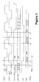
- clock signals There are two clocks, one clock being a square wave signal at a frequency not greater than 2 million Hertz (periods per second) and the second being a similar square wave whose transitions occur approximately mid-way between those of the first. These signals are referred to by the names CLKP and CLKQ respectively in Figures 1 and 2.
- CLKP and CLKQ respectively in Figures 1 and 2.
- the use of two clocks permits the connected devices to be so designed as to reject spurious transitions caused by imperfect signal transmission or noise injection, as when one clock is in a given state then only one transition of the other clock is expected and its sense is pre-determined.
- the two signals CLKP and CLKQ are transmitted in the specific implementation cited as an example in a balanced form, in that two signal lines of the bus are used for each clock, sent on the bus in both true and inverted forms.
- Control signals are transmitted on the bus, being generated by the controller.
- these will include BIOW, the command to the addressed module to accept a data pattern for storage or some other action, BIOR, a command to the addressed module to supply data to the controller, and BRES, a general command to all stations to adopt a standard state, which is typically the quiescent state assumed when the system starts up.
- BIOW the command to the addressed module to accept a data pattern for storage or some other action
- BIOR a command to the addressed module to supply data to the controller
- BRES a general command to all stations to adopt a standard state, which is typically the quiescent state assumed when the system starts up.
- These signals are, and have been for many years, common practice. They are associated with selection signals and with data paths, which in the example are separate groups of signal lines. This is preferable for electrical transmission reasons to the commonly used shared data path over which data travels both to and from the controller.
- a further advantage of separation in the implementation cited as an example is that the protocol requires that, in cycles in which BIOW is set, the data sent out by the controller on the "WRITE DATA" path is returned to it, in the second phase of the transaction, on the "READ DATA” path.
- the controller checks that the data has not been corrupted, and on detecting any corruption may take appropriate measures, such as repeating the operation, raising an alarm, or opening a safety interlock.
- the selection of the module is a vital part of the bus transaction, and is achieved by transmission, by the controller, of a selection code. In the typical case this will have several binary digits, and in the example there are two digits to specify from one to four assemblies of modules, commonly called crates or racks, and four binary digits to specify 16 possible modules in each such assembly.
- this code can only be received by one module, for each code pattern transmitted as an address code, and only one module can be selected.
- the transformation may be arranged in various ways, and in the specific implementation cited as an example the well-known Gray coding principle is adopted, whereby the binary state of a single binary digit of the address code is inverted in the bus wiring in between each successive pair of module positions along the bus. This inversion is facilitated by the transmission of each signal on two lines of the bus, in true and inverted form, such that inversion of the sense of a binary digit is achievable by simply interchanging the two wires.
- the advantage of this selection scheme over those more frequently used is that no switches or links are employed to set the module address code, and a common source of errors is thereby removed.
- control signals, selection and sub-address signals, and data to the sent by the controller, if any, are transmitted on the bus at time t1, shortly after a false-to-true transition of CLKP, as shown in Figure 1. They are normally maintained for approximately two periods of the CLKP waveform.
- Cross-hatching in the timing diagrams is meant to show times at which the signals are indeterminate and to illustrate that some of the bus signals need not be established very quickly, or at very precisely determined times: these signals are primarily the data and sub-address signals.
- the invention specifies a method of detecting errors in module selection. These may originate from electrical faults in the addressed modules or in the controller, or in the wiring of the bus. They also be caused by transient electrical or electro-magnetic interference signals, introduced into the system at various points. The method combines two elements.
- the selected module must immediately supply a unique code called the "Module Position Code” (MPC). This code is defined for each address and can be checked by the controller.
- MPC Module Position Code
- the module must supply a drive to an analog line, called AX* in the timing diagram, which in the example is performed by switching a resistor to ground.
- AX* an analog line
- the controller the lack of such a resistor may be detected, and the presence of two or more resistors may also be detected. The controller may be sure, at the completion of the first phase of the transaction, that one and only one module has been selected, and that it is the required module.
- the module produces the MPC and AX* signals at time t2, after t1 and shortly after a false-to-true transition of CLKQ.
- the Module Position Code of each module is generated automatically at the end of the RESET procedure, when the system is being initialised.
- An 8-bit MPC is then generated from the code at the selection lines of the bus, and each module has a different MPC.
- the MPC is sent on the data bus lines which are defined for "READ DATA". It is sent to the controller in the first phase of the transaction, after time t2 and before time t3, and data is transmitted in the second phase, after time t3 and until the controller has removed the control signals BIOR or BIOW, as shown in Figure 1.
- the bus timing is so specified as to permit the controller, on detecting a selection error, to cut short the transaction as shown in the timing diagram, Figure 2, at about time t3.
- the design of the modules will be such as to place any possible action commanded by the controller very late in each transaction, typically between times t4 and t5 shown in Figure 1 so that a premature termination of the command signals will prevent such actions from ocurring.
- timing diagrams are simplified in that they do not show the effects of finite transmission times along the bus, which will cause the timing relationships at various points to be slightly different, without altering the principle of operation. In a practical implementation the effects of delays along the bus will be taken into account when determining the precise specifications for bus operation in respect of permissible timings.
- the analog signal line which is employed to detect the number of selected modules is biassed by the controller, which endeavours to supply a current of approximately 10 mA to the signal line, but is not able to establish a potential of more than 3.2 volts on the line, measured with respect to the common or gound potential to which all signals on the bus are referenced.
- Each module when it is selected, connects a resistor of value approximately 185 ohms between the analog signal line and the common ground. If one and only one module is selected the analog line will take up a potential of approximately 1.85 Volts, while if two modules are selected, on account of a malfunction of any nature, the potential of the analog line will fall to less than 1.0 Volt. If no module is selected the potential on the analog line will stay at the potential assumed when no operations are taking place, at about 3 Volts.
- Each module may require to have several internal features selected, for reading or writing data or commands.
- seven sub-address signal lines are provided on the bus, such that up to 128 internal features may be distinguished in each module.
- these are not further checked, as it is assumed that the consequences of, and difficulty of recuperating from, errors in sub-addressing are less serious than errors in selecting the module itself. Nevertheless, two measures are proposed. Firstly, in cases where data registers have safety or other major implications, their addresses are selected such that at least two binary digits differ, so that a single-digit fault will not produce a valid sub-address.
- an additional bus signal line is employed to signal the detection of module errors. This line is driven at any time during the transaction by the module which is selected, to the true or false states, and in particular, during the second part of the transaction, will be driven true if an invalid sub-address is found.
- the controller may then, on detecting a module error, indicate an alarm condition, to be dealt with as appropriate.
- One sub-address is reserved for testing, and is considered valid while having no effect. This sub-address may have various data patterns sent to it, and the integrity of the data paths in both directions may be checked from time to time.
- Figure 3 shows the block diagram of the bus interface in a module corresponding to the specific embodiment cited as an example. Signals of the bus are those on the left hand side of the diagram.
- the balanced clock signals pass to comparators 2 and the comparator outputs CLKP and CLKQ are connected to programmable logic device 1.
- Clocks CLKP and CLKQ are square waves at 1.8 MHz approximately.
- the selection codes arrive in true and complement forms, as SN0 to SN3 inclusive to select one position of 16 and SC0 with SC1 to define a crate.
- the inverted inputs are identified as SN0* to SN3*, and SC0* plus SC1*. Only one possible pattern will produce an output from the decoder 3, which is connected to the control logic device 1.
- This logic device is programmed to control the various events which occur when a module is selected and it employs an internal finite state machine driven by the two clock inputs to determine the timing of each action.
- the module position code register 6 in Figure 3 is loaded with an 8-bit pattern derived from the six selection lines and their inverted forms, about one microsecond after the end of the RESET signal.
- This pattern is the Module Position Code (MPC), and is created in a simple logic array 4.
- a gating signal is generated during the first part of the transaction, and causes the MPC code word to pass onto the internal 8-bit data bus 10 and into the register 11, which drives the data path to the controller.
- the transistor 9 connects the resistor 8 betwen the analog bus line identified as AX* and the common ground potential.
- a data register 5 takes the data arriving on the data path from the controller, and stores it for the rest of the transaction. This is only the case for "writing" data from the controller into some feature of the module, in this case the register or registers shown as item 12. The data must pass from the register 5 to the register(s) 12 over the internal 8-bit data bus 10, and this will take place in the later part of the operation, when the MPC is no longer transmitted to the bus 10 from register 6.
- this data is passed onto the internal data bus from an input register 7, selected according to the sub-address code, and then passes into the read data register 11, from which it is transmitted to the controller over the read data path. This takes place after time t3 in the timing diagram Figure 1, after the period when the MPC is transmitted to the controller on the same data path.
- a gating system ensures that this data path is only driven when the module is selected, as it is shared with other modules on the bus.
- the data arriving at 5 from the controller is sent to the output register(s) 12, again after time t3, and also passes via the register 11 back to the controller, where it is compared with the data sent by the controller.
- the selection and sub-address signals will typically be derived from a set of computer address lines, and the command signals from those issued by the computer to the control interface.
- the data output lines will be driven when data is transmitted.
- Data input lines will be wired to line receivers, and then to intermediate registers which store the MPC and the returned data respectively, at suitable instants of time (shortly before t3 and shortly after t5 in Figure 1) in the operation.
- the MPC is compared with the MPC which is expected, for the specific module which should have been selected, and any discrepancy is detected.
- the analog line AX* is conected to two high-speed comparators, with threshold voltages set to approximately 2.4 Volts and 1.3 Volts: a potential in excess of 2.4 Volts is interpreted as showing no module responding as being selected, and a potential below 1.3 Volts as indicating multiple module selection. Errors in either the MPC code or the AX* level will cause the write command BIOW to be terminated prematurely, at about t3 as shown in the timing diagram, Figure 2.
Landscapes
- Engineering & Computer Science (AREA)
- Theoretical Computer Science (AREA)
- Physics & Mathematics (AREA)
- General Engineering & Computer Science (AREA)
- General Physics & Mathematics (AREA)
- Quality & Reliability (AREA)
- Debugging And Monitoring (AREA)
- Information Transfer Systems (AREA)
Applications Claiming Priority (2)
| Application Number | Priority Date | Filing Date | Title |
|---|---|---|---|
| GB9405499A GB2288953B (en) | 1994-03-21 | 1994-03-21 | Self-testing secure-transaction computer input-output bus |
| GB9405499 | 1994-03-21 |
Publications (2)
| Publication Number | Publication Date |
|---|---|
| EP0675437A2 true EP0675437A2 (de) | 1995-10-04 |
| EP0675437A3 EP0675437A3 (de) | 1996-05-08 |
Family
ID=10752210
Family Applications (1)
| Application Number | Title | Priority Date | Filing Date |
|---|---|---|---|
| EP95104014A Withdrawn EP0675437A3 (de) | 1994-03-21 | 1995-03-18 | Selbstprüfender transaktionssicherer Computer-Ein-Ausgabe-Bus. |
Country Status (2)
| Country | Link |
|---|---|
| EP (1) | EP0675437A3 (de) |
| GB (1) | GB2288953B (de) |
Cited By (1)
| Publication number | Priority date | Publication date | Assignee | Title |
|---|---|---|---|---|
| FR2821453A1 (fr) * | 2001-02-26 | 2002-08-30 | Valeo Climatisation | Procede d'identification des noeuds d'un reseau informatif dans une installation de climatisation de vehicule automobile, et installation de climatisation faisant application du procede |
Family Cites Families (8)
| Publication number | Priority date | Publication date | Assignee | Title |
|---|---|---|---|---|
| DE2423260A1 (de) * | 1974-05-14 | 1975-11-20 | Siemens Ag | Verfahren und schaltungsanordnung zur pruefung von daten verarbeitenden anlagen, insbesondere fernsprechvermittlungsanlagen mit ueber ein busleitungssystem an eine steuerzentrale angeschlossenen peripheren einrichtungen |
| GB2103397A (en) * | 1981-07-31 | 1983-02-16 | Philips Electronic Associated | Digital data aparatus with memory selection |
| US4675769A (en) * | 1985-11-15 | 1987-06-23 | Data General Corporation | Electronic board identification |
| US4989202A (en) * | 1988-10-14 | 1991-01-29 | Harris Corporation | ISDN testing device and method |
| US5077670A (en) * | 1988-12-28 | 1991-12-31 | Nissan Motor Company, Limited | System and method applicable to vehicles for communicating between data processing stations |
| US5132905A (en) * | 1988-12-28 | 1992-07-21 | Nissan Motor Company Limited | System and method applicable to vehicles for communicating between data processing stations |
| JP2547654B2 (ja) * | 1990-06-29 | 1996-10-23 | 三洋電機株式会社 | データ処理装置 |
| AU648648B2 (en) * | 1991-04-15 | 1994-04-28 | Hochiki Kabushiki Kaisha | Method of detecting transmission error in disaster prevention supervisory system |
-
1994
- 1994-03-21 GB GB9405499A patent/GB2288953B/en not_active Expired - Fee Related
-
1995
- 1995-03-18 EP EP95104014A patent/EP0675437A3/de not_active Withdrawn
Cited By (4)
| Publication number | Priority date | Publication date | Assignee | Title |
|---|---|---|---|---|
| FR2821453A1 (fr) * | 2001-02-26 | 2002-08-30 | Valeo Climatisation | Procede d'identification des noeuds d'un reseau informatif dans une installation de climatisation de vehicule automobile, et installation de climatisation faisant application du procede |
| WO2002069149A1 (fr) * | 2001-02-26 | 2002-09-06 | Valeo Climatisation | Procede d"identification des noeuds d"un reseau informatif dans une installation de climatisation de vehicule automobile |
| US7869918B2 (en) | 2001-02-26 | 2011-01-11 | Valeo Climatisation | Method of identifying nodes in a computer network in a motor vehicle air conditioning installation |
| US8554405B2 (en) | 2001-02-26 | 2013-10-08 | Valeo Systemes Thermiques | Method of identification of the nodes of a computer network in an air conditioning installation of a motor vehicle, and air conditioning installation using the method |
Also Published As
| Publication number | Publication date |
|---|---|
| GB2288953A (en) | 1995-11-01 |
| GB2288953B (en) | 1998-08-05 |
| EP0675437A3 (de) | 1996-05-08 |
| GB9405499D0 (en) | 1994-05-04 |
Similar Documents
| Publication | Publication Date | Title |
|---|---|---|
| US5068851A (en) | Apparatus and method for documenting faults in computing modules | |
| US4085448A (en) | Data communication bus structure | |
| US4366535A (en) | Modular signal-processing system | |
| US4630041A (en) | Enhanced reliability interrupt control apparatus | |
| US4670876A (en) | Parity integrity check logic | |
| US5163138A (en) | Protocol for read write transfers via switching logic by transmitting and retransmitting an address | |
| US4596014A (en) | I/O rack addressing error detection for process control | |
| US3810577A (en) | Error testing and error localization in a modular data processing system | |
| CA1267224A (en) | Apparatus and method for detecting time-related faults | |
| JPS63273142A (ja) | クロス接続形検査回路及びそのための集積回路 | |
| US4819205A (en) | Memory system having memory elements independently defined as being on-line or off-line | |
| US4959836A (en) | Register robustness improvement circuit and method | |
| US4700346A (en) | Self-checking, dual railed, leading edge synchronizer | |
| US4017829A (en) | Method and circuit arrangement for testing data processors | |
| CA1187957A (en) | Vital communication system for transmitting multiple messages | |
| US4831516A (en) | Data transmission system between a main CPU board having a wait signal generating latch and a plurality of CPU boards | |
| US4926427A (en) | Software error detection apparatus | |
| US6125454A (en) | Method for reliably transmitting information on a bus | |
| US5436856A (en) | Self testing computer system with circuits including test registers | |
| US6374365B1 (en) | Arrangement for operating two functionally parallel processors | |
| GB2288953A (en) | Self-testing secure-transaction computer input-output bus | |
| US5444722A (en) | Memory module with address error detection | |
| US5311524A (en) | Fault tolerant three port communications module | |
| US3750110A (en) | Data transfer systems | |
| US3649963A (en) | Error detection arrangement for register-to-register data transmission |
Legal Events
| Date | Code | Title | Description |
|---|---|---|---|
| PUAI | Public reference made under article 153(3) epc to a published international application that has entered the european phase |
Free format text: ORIGINAL CODE: 0009012 |
|
| AK | Designated contracting states |
Kind code of ref document: A2 Designated state(s): DE FR GB |
|
| PUAL | Search report despatched |
Free format text: ORIGINAL CODE: 0009013 |
|
| AK | Designated contracting states |
Kind code of ref document: A3 Designated state(s): DE FR GB |
|
| 17P | Request for examination filed |
Effective date: 19961101 |
|
| RBV | Designated contracting states (corrected) |
Designated state(s): DE FR |
|
| 17Q | First examination report despatched |
Effective date: 20000323 |
|
| STAA | Information on the status of an ep patent application or granted ep patent |
Free format text: STATUS: THE APPLICATION HAS BEEN WITHDRAWN |
|
| 18W | Application withdrawn |
Withdrawal date: 20000529 |