EP0676684A2 - Inkrementalausgangschaltung zur Stromversorgung - Google Patents
Inkrementalausgangschaltung zur Stromversorgung Download PDFInfo
- Publication number
- EP0676684A2 EP0676684A2 EP95301859A EP95301859A EP0676684A2 EP 0676684 A2 EP0676684 A2 EP 0676684A2 EP 95301859 A EP95301859 A EP 95301859A EP 95301859 A EP95301859 A EP 95301859A EP 0676684 A2 EP0676684 A2 EP 0676684A2
- Authority
- EP
- European Patent Office
- Prior art keywords
- current
- output
- voltage
- circuit
- input
- Prior art date
- Legal status (The legal status is an assumption and is not a legal conclusion. Google has not performed a legal analysis and makes no representation as to the accuracy of the status listed.)
- Withdrawn
Links
Images








Classifications
-
- G—PHYSICS
- G05—CONTROLLING; REGULATING
- G05F—SYSTEMS FOR REGULATING ELECTRIC OR MAGNETIC VARIABLES
- G05F3/00—Non-retroactive systems for regulating electric variables by using an uncontrolled element, or an uncontrolled combination of elements, such element or such combination having self-regulating properties
- G05F3/02—Regulating voltage or current
- G05F3/08—Regulating voltage or current wherein the variable is DC
- G05F3/10—Regulating voltage or current wherein the variable is DC using uncontrolled devices with non-linear characteristics
- G05F3/16—Regulating voltage or current wherein the variable is DC using uncontrolled devices with non-linear characteristics being semiconductor devices
- G05F3/20—Regulating voltage or current wherein the variable is DC using uncontrolled devices with non-linear characteristics being semiconductor devices using diode- transistor combinations
- G05F3/24—Regulating voltage or current wherein the variable is DC using uncontrolled devices with non-linear characteristics being semiconductor devices using diode- transistor combinations wherein the transistors are of the field-effect type only
Definitions
- the present invention relates to circuits which generate an incremental output source current dependent on an input voltage level.
- Process improvements allow for the fabrication of the circuits and chips into increasing densities and quantities with enhanced reliability characteristics. Structural improvements allow for greater circuit performance and control of power consumption with enhanced reliability as well.
- the advancement of chip density has led to the reduction of the size of the individual circuit components contained on the chip. These integrated-circuit chip densities have grown because of the ability to decrease the size of the individual devices (electronic components) contained on each chip.
- the benefits of the reduction in the size of the individual chip components have allowed for an increase in the circuit performance level because of the increased circuit speed. With the less distance the current must travel from component to component, the information contained therein can be processed within the chip in a shorter amount of time. More importantly, with density improvements the chip's circuits require less power to operate.
- the present invention provides a novel incremental output current generation circuit is disclosed herein.
- a reference current and a reference voltage are established by the combination of a transistor and a current mirror which follow the values of a bias current.
- the reference current is then multiplied by a current multiplication means.
- a set of predetermined voltage reference points are established in a voltage referencing means with sufficient current being supplied thereto by the current multiplication means.
- the ramping values of an input voltage are then compared to the established voltage referencing points in the comparison means the outputs of which flag the highest voltage reference value which the input voltage exceeded.
- These comparitor outputs trigger in a current generation means predetermined incremental current fractions of the established reference current.
- These incremental currents are delivered to the output as the output current. In such a manner, an incremental output source current is generated which is dependent on an input voltage level and predetermined incrementally by the value of an established reference current.
- a reference current and a reference voltage establish bias current by the combination of a transistor and a current mirror.
- the reference current is then multiplied in a current multiplication means.
- a set of predetermined voltage reference points are established in a voltage referencing means with sufficient current being supplied thereto by the current multiplication means.
- the ramping values of an input voltage are then compared to the voltage reference points in a comparison means the outputs of which flag the highest voltage reference value which the input voltage exceeded. These outputs are then directed into a latching means for holding the signal steady and a reset means for establishing stable initial conditions in the latching means.
- the latching means outputs trigger a predetermined incremental values of the reference current which is delivered at the output as the output current. In such a manner, an incremental output current is generated which is dependent on the ramping values of an input voltage and predetermined incrementally by the value of an established reference current.
- the present invention is directed to circuits which generate an incremental output source current by sensing an input voltage and predetermined incrementally by the value of an established reference current.
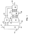
- FIG. 1 is a block diagram illustration of one embodiment of the incremental output current generation circuit of the present invention.
- a reference generation means 10 accepts a bias current 12 and a low voltage power supply 14 both connected to a common ground as shown in order to establishes a reference current IR therethrough and a reference voltage VR across lines 16.
- the reference voltage VR is dependent on the reference current which in turn is linked to the value of the bias current IBIAS.
- a current multiplication means 18 uses the reference current IR as a baseline to be multiplied. The multiplied current is driven into the voltage referencing means 24 over 22.
- the voltage across 16 is also made available across 20.
- the voltage referencing means 24 is tied to a common ground with the reference generation means 10 by 26.
- the voltage referencing means 24 establishes a series of voltage reference points therethrough which are directed across a plurality of outputs 30 which tie into the comparitor means 28 for comparison with the ramping level of an input voltage 38.
- the plurality of outputs 34 of the comparitor means 28 are directed into a current output means 32 which quickly generates a stable output current 36. This output current is tied to the level of the input voltage 38. With such a circuit, because the output current 36 can be quickly ramped and held stable external circuit turn-on time can be made much quicker.
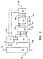
- FIG. 2 is a block diagram illustration of the preferred embodiment of the incremental output current generation circuit of Figure 1 incorporating a latching means 40 and a reset means 42.
- the outputs 34 tie the voltage comparison means 28 to the latching means 40.
- At least one additional output 44 from the comparitor means 28 ties into the reset means 42.
- the reset means has at least one output 46 directed into the latching means 40 in order to effectuate a reset of the latches.
- Outputs 48 connect the latching means to the current output means 32 in order to trigger the current output in a manner as with that of Figure 1.
- points such as those labeled A1, A2, and A3 are for connecting the circuit configuration of one diagram to that of another wherein like labeled connection points are designated to be electrically joined.
- point A1 of Figure 3A is only connected to point A1 of Figure 4.
- Figure 3A is a diagram of one embodiment of the reference generation means 10 of Figures 1 and 2 incorporating a single transistor T1 and a two transistor configured current mirror means 50.
- a supply voltage 14 is connected to transistor T1.
- a bias current, labeled IBIAS, is made to flow in the direction of the accompanying arrow to ground.
- the source voltage can be any power supply preferably +5V.
- An output voltage, labeled V1 is available as a relatively stable voltage source for use outside the circuit of the present invention.
- V1 can be used in conjunction with other transistors for mirroring current levels elsewhere in order to force the same current levels in another circuit.
- a pair of transistors labeled T2 and T3, are arranged in a mirror configuration. Since the configuration of the mirroring of current is well known in the arts and one skilled in this art should already be familiar with its construction, functionality, and purpose a further explanation of the particulars of the function of the mirror configuration is omitted herein. However, what is important in this regard is that I1 is the same as the bias current IBIAS. If T3 is made the same as T2 then I2 is equal to I1 and the amount of reference current IR that is made to flow through T1 will be the same as that of I2.
- Figure 3B is a diagram of an alternative embodiment of the reference generation means 10 of Figures 1 and 2 illustrating a four transistor configured current mirror means 52 wherein a cascode configuration is effectuated by the addition of transistors T4 and T5.
- the effect of the addition in this embodiment is to make the configuration of the current mirror means 50 of Figure 3A less sensitive to the kinds of noise typically associated with the flow of the bias current therethrough and to make the overall current mirror configuration less sensitive to fluctuations in the level of the bias voltage connected there across.
- an increased element of stability is added the overall circuit of the present invention.
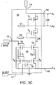
- Figure 3C is a diagram of the reference generation means 10 of Figures 1 and 2 incorporating an additional top transistor T7 and a five transistor configured current mirror means 53 with a sleep-mode means 17.
- transistor T1 which is cascoded by transistor T7.
- the addition of this transistor as configured affords the top portion of the circuit of the present invention the added protection from unwanted fluctuations and variations in the level of the source voltage power supply 14 with respect to ground. This adds stability to the reference voltage developed across 16 by the flow of the reference current therethrough.
- another voltage reference point, labeled V2 can be made available for use in other circuits in a fashion similar to that of V1.
- the sleep-mode means 17 comprises a transistor T6 which is connected between transistors T4 and T5 and which is tied at one end to ground and a state generation line. As shown, transistor T6 is connected to a state generation line, designated SLEEP.
- SLEEP state generation line
- transistor T6 when the SLEEP line goes HIGH, for instance to +5V, transistor T6 is turned ON in effect shunting the bias current directly to ground. This inhibits the mirror of current 11 into 12 thereby prohibiting the flow of the reference current.
- a mechanism can be added to the mirror such that the draw of the reference current can be turned ON/OFF. If the reference current does not flow then no reference voltage is developed across lines 16. This shuts down the current multiplication means 18.
- this particular embodiment enables the addition of a level of control to the functionality and operability of the current mirror and to the reference generation means 10 and therefore to the rest of the circuit of the present invention.
- Other configurations which also effectuate an enablement of the reference current and reference voltage by enabling/disabling the reference generation means 10 are envisioned herein and are to be considered equivalent to this particular embodiment and within the scope of the present invention.
- Figure 4 is a diagram of one embodiment of the current multiplication means 18 of Figures 1 and 2.
- Connecting points A1 and A2 are electrically connected to points A1 and A2 of Figure 3A or in alternative embodiments to similarly labeled points of Figures 4B or 4C.
- Connecting point B1 is connected to B1 of Figure 5 and points C1 and C2 are connected to similarly labeled points of Figures 8 and 10.
- the current multiplication means 18 comprises a bank of 4 transistors labeled T10, T11, T12, and T13.
- This bank of transistors is connected in parallel to effectuate a multiplication of the established reference current IR.
- the reference voltage which is connected across points A1 and A2, is also established across C1 and C2.
- each of the four transistors have been chosen to be equal. In other words, with the reference voltage across the line 16 junction, each of the four transistors can enable a similar level of the reference current therethrough at their respective outputs.
- each of these transistors have been chosen to have the same characteristics such that each can pass the reference current. Thus, each transistor will effectuate a 1X multiplication of the reference current IR given the reference voltage. Thus, the combination of the four transistors taken together enables a 4X multiplication of the reference current.
- the 4X multiplied reference current 4XIR is directed into the voltage referencing means 24 along 22 to B1.
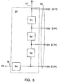
- Figure 5 is a diagram of one embodiment of the voltage referencing means 24 of Figures 1 and 2.
- the outputs, collectively designated as 30, tie the voltage referencing means to the comparitor means 28.
- the diagrams of Figures 1 and 2 show multiple lines at 30 because any number of outputs could be taken depending on the configuration.
- Line 26 connects a ground with the reference generator means 10.
- a total of four resistive elements, labeled R1, R2, R3, and R4 create different voltage referencing values at B2, B3, B4, and B5.
- the example voltage points associated therewith are labeled in brackets.
- Resistive element R4 ties to ground to provide an appropriate drain. Connecting point B1 is connected to B1 of Figure 4 and A3 is connected to A3 of either Figures 3A, 3B, or 3C.
- a series of voltage reference points are established to be used in conjunction with the comparator means 28 to which the ramping level of an input voltage 38 will be compared against.
- the successive voltage reference points be of increasing value from bottom to top (as illustrated). For instance, at point B3 the voltage would be less than that at point B2 because of the drop across the resistive element R1 therebetween.
- the resistive elements can be selected to provide the desired voltage reference points to which the ramping level of the input voltage 38 can be compared against. In this embodiment only four reference levels have been designated. In brackets are example voltage reference levels which will be used herein to help one understand this invention by way of example.
- any number of voltage reference points could be established by the voltage referencing means in order to achieve whatever degree of refinement in the detection of the ramping voltage level of the input voltage 38. For instance, if 10 gradations were desired then 10 distinct referencing points would have to be established separated by differing resistive elements between each point and sufficient current would have to be generated by the current multiplication means 18 and made available at B1. This is why the embodiments of Figures 1 and 2 illustrate a plurality of outputs at 30. Therefore, other embodiments of the voltage referencing means establishing any number of voltage referencing points (even 1) for comparison to the level of the input voltage 38 in the comparitor means are to be considered within the scope of the present invention.
- Figure 6 is a diagram of one embodiment of the comparator means 28 of Figure 1.
- the voltage reference value produced as a result of the function of the voltage referencing means. Since embodiment of the voltage referencing means 24 of the present invention was configured to have a total of 4 reference points a matching number of 4 comparators have been implemented. Connecting points B2, B3, B4, and B5 tie to the corresponding points of the voltage referencing means of Figure 4.
- This embodiment has 4 comparators, labeled 1, 2, 3, and 4 with each having the IN line tied directly to the corresponding reference outputs and with each having the REF line tied to the input line of the input voltage for comparison purposes.
- the outputs connect with either the current output means 32 of the embodiment of Figure 1 or with the latching means 40 and the reset means 42 of the embodiment of Figure 2.
- the diagrams of Figures 1 and 2 show multiple lines at 34 because any number of outputs could be taken depending on the configuration. To the right in brackets are the states of the corresponding outputs which will be explained as part of an example provided herein.
- the designated referencing values have tied to the IN of each comparator while the input voltage 38 has been tied to each REF input in order to effectuate the comparisons.
- the outputs of the referencing means and the input voltage could be first inverted then tied to the opposite comparitor inputs.
- other configurations with varying amounts and kinds of comparators can be used in the alternative to effectuate the same result. For instance, a differing number such that a 1-to-many or a many-to-1 ratio of comparators to available referencing means outputs could be implemented. Therefore, other embodiments having alternative configurations wherein the defined number of referencing outputs are compared with the ramping level of the input voltage are to be considered envisioned herein and within the scope of the present invention.
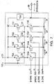
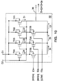
- the upper row of four transistors labeled T24, T23, T22, and T21, are connected to points C1 and C2 and thus to the reference voltage VR.
- the bottom bank of transistors labeled T25, T26, T27, and T28 act as switches. These p-channel devices, when turned on by a LOW signal, let the current flow therethrough.
- the bottom bank of transistors are configured such that when their respective lines D1-D4 are at a LOW state the current is enabled to flow. Conversely, when lines D1-D4 are at a HIGH state the current does not flow.
- a reference current and a reference voltage which followed the values of the bias voltage and bias current were established by the combination of a transistor and a current mirror means.
- the reference current was multiplied by a factor of four.
- a set of predetermined voltage reference points were established in the voltage referencing means and sufficient current supplied there across by the current multiplication means.
- the ramping values of the input voltage 38 were then compared to the voltage reference points in the comparison means the outputs of which flagged the highest voltage reference point which the value of the input voltage crossed.
- these comparitor outputs trigger predetermined incremental values of the reference current to be delivered to the output. In such a manner, an incremental output source current is generated which is dependent on an input voltage level and predetermined incrementally by the value of an established reference current.
- the level of the input voltage ramps up it passes the 2.3V reference point.
- the REF becomes higher than INV thereby forcing the output of comparator 4 line D4 to HIGH.
- the value of REF becomes greater than that of INV at comparitor 3 forcing the output of comparator 3 line D3 to HIGH.
- the final ramping level of the input voltage was greater than 2.7V but less than 2.9V.
- the final states as indicated in brackets at D1 and D2 are LOW and D3 and D4 are set HIGH.
- the start-up states of the NOR do not have to be commonly set because of the reset means 35.
- the functionality of a NOR gate is such that the output is LOW if any (or both) of the inputs are HIGH else the output is HIGH. Since the desired initial state is LOW, in order to effectuate a reset both of the input lines of each of the NOR gates must be made LOW. As discussed, upon start-up the output of each of the 4 comparators is set LOW. So the reset must set the other input lines to LOW to allow reaction to other signals. When the output, at line 46, of the reset invertor is HIGH nothing can happen in the latching means.
- the states of lines D1-D4 are LOW, LOW, HIGH, and HIGH respectively.
- the corresponding states of lines E1-E3 are HIGH, HIGH, and LOW respectively, as is shown.
- latching means and reset means of the preset invention could effectuate a similar output at points E1-E3 using other means such as NAND gates or transistors or other circuitry.
- Other embodiments thus envisioned would also have a means associated therewith to effectuate a reset if that particular configuration was such that the initial states had to be effectively known and controllable. It is envisioned that some configurations could function without the reset means entirely.
- the latching means could have a locking mechanism added to it in order to prevent jitter when and if the input voltage drifts. Therefore, other embodiments of the latching means with or without the accompanying reset means are to be considered within the scope of the present invention.
- FIG. 8 is a table of the ratios of one configuration of the top bank of the current output means.
- transistor T24 when switched will effectively deliver 20 units of IR to the output as I4.
- Transistor T23 will effectively deliver 12 units of IR to the output as I3.
- Transistor T32 will deliver 8 units of IR to the output as I2.
- transistor T21 will always deliver a total of 24 units of IR to the output as I1.
- at least 3/4 the value of IR will at least be available as the output current 36.
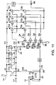
- Figure 12 is a diagram of the preferred embodiment of the circuit of the present invention incorporating the individual configurations of Figures 3A, 4, 5, 6B, 9, and 10.
- a reference current and a reference voltage which followed the values of the bias voltage and current were established by the combination of a transistor and a current mirror means.
- the reference current was multiplied by a factor of four.
- a set of predetermined voltage reference points were established in the voltage referencing means and sufficient current supplied there across by the current multiplication means.
- the ramping values of the input voltage were then compared to the voltage reference points in the comparison means the outputs of-which flagged the highest voltage reference point which the value of the input voltage crossed. These outputs are directed into a latching means for holding the signal steady and a reset means.
- these outputs trigger predetermined incremental values of the reference current to be delivered to the output as the output current. In such a manner, an incremental output source current is generated which is dependent on an input voltage level and predetermined incrementally by the value of an established reference current.
- the output current can be quickly ramped to a predetermined level the overall time required to test a die can be shortened because the circuit turn-on time is much quicker.
- this output current can also be used to adjust the changing current in the Phase Detector because that circuit typically has a charge pump in it.
Landscapes
- Engineering & Computer Science (AREA)
- Microelectronics & Electronic Packaging (AREA)
- Physics & Mathematics (AREA)
- Nonlinear Science (AREA)
- Electromagnetism (AREA)
- General Physics & Mathematics (AREA)
- Radar, Positioning & Navigation (AREA)
- Automation & Control Theory (AREA)
- Amplifiers (AREA)
- Manipulation Of Pulses (AREA)
- Semiconductor Integrated Circuits (AREA)
- Control Of Electrical Variables (AREA)
- Dc-Dc Converters (AREA)
- Logic Circuits (AREA)
- Analogue/Digital Conversion (AREA)
Applications Claiming Priority (2)
| Application Number | Priority Date | Filing Date | Title |
|---|---|---|---|
| US226163 | 1988-07-29 | ||
| US08/226,163 US5608314A (en) | 1994-04-11 | 1994-04-11 | Incremental output current generation circuit |
Publications (2)
| Publication Number | Publication Date |
|---|---|
| EP0676684A2 true EP0676684A2 (de) | 1995-10-11 |
| EP0676684A3 EP0676684A3 (de) | 1998-03-04 |
Family
ID=22847820
Family Applications (1)
| Application Number | Title | Priority Date | Filing Date |
|---|---|---|---|
| EP95301859A Withdrawn EP0676684A3 (de) | 1994-04-11 | 1995-03-21 | Inkrementalausgangschaltung zur Stromversorgung |
Country Status (5)
| Country | Link |
|---|---|
| US (1) | US5608314A (de) |
| EP (1) | EP0676684A3 (de) |
| JP (1) | JPH086655A (de) |
| KR (1) | KR950035049A (de) |
| TW (1) | TW279284B (de) |
Cited By (1)
| Publication number | Priority date | Publication date | Assignee | Title |
|---|---|---|---|---|
| WO2003075451A1 (de) * | 2002-03-04 | 2003-09-12 | Infineon Technologies Ag | Abstimmbares, kapazitives bauteil und lc-oszillator mit dem bauteil |
Families Citing this family (2)
| Publication number | Priority date | Publication date | Assignee | Title |
|---|---|---|---|---|
| US6362767B1 (en) * | 1999-03-22 | 2002-03-26 | The Board Of Trustees Of The Leland Stanford Junior University | Methods for simultaneous analog-to-digital conversion and multiplication |
| JP4177364B2 (ja) * | 2005-09-12 | 2008-11-05 | 三菱電機株式会社 | 定電圧制御装置 |
Family Cites Families (6)
| Publication number | Priority date | Publication date | Assignee | Title |
|---|---|---|---|---|
| US3832624A (en) * | 1973-09-06 | 1974-08-27 | Allis Chalmers | Group blanking control for cycloconverter |
| JPS592410A (ja) * | 1982-06-28 | 1984-01-09 | Sony Corp | 電流増幅器 |
| KR880700349A (ko) * | 1984-10-01 | 1988-02-22 | 마이클 와이·엡스타인 | 전류원을 구비한 집적회로 |
| GB2222884A (en) * | 1988-09-19 | 1990-03-21 | Philips Electronic Associated | Temperature sensing circuit |
| US5355077A (en) * | 1992-04-27 | 1994-10-11 | Dell U.S.A., L.P. | High efficiency regulator with shoot-through current limiting |
| US5291446A (en) * | 1992-10-22 | 1994-03-01 | Advanced Micro Devices, Inc. | VPP power supply having a regulator circuit for controlling a regulated positive potential |
-
1994
- 1994-04-11 US US08/226,163 patent/US5608314A/en not_active Expired - Fee Related
- 1994-08-17 TW TW083107534A patent/TW279284B/zh active
-
1995
- 1995-03-21 EP EP95301859A patent/EP0676684A3/de not_active Withdrawn
- 1995-04-04 KR KR1019950007865A patent/KR950035049A/ko not_active Withdrawn
- 1995-04-10 JP JP7084084A patent/JPH086655A/ja not_active Withdrawn
Cited By (2)
| Publication number | Priority date | Publication date | Assignee | Title |
|---|---|---|---|---|
| WO2003075451A1 (de) * | 2002-03-04 | 2003-09-12 | Infineon Technologies Ag | Abstimmbares, kapazitives bauteil und lc-oszillator mit dem bauteil |
| US6995626B2 (en) | 2002-03-04 | 2006-02-07 | Infineon Technologies Ag | Tunable capacitive component, and LC oscillator with the component |
Also Published As
| Publication number | Publication date |
|---|---|
| JPH086655A (ja) | 1996-01-12 |
| EP0676684A3 (de) | 1998-03-04 |
| KR950035049A (ko) | 1995-12-30 |
| US5608314A (en) | 1997-03-04 |
| TW279284B (de) | 1996-06-21 |
Similar Documents
| Publication | Publication Date | Title |
|---|---|---|
| US6084437A (en) | Logic circuit utilizing pass transistors and logic gate | |
| US5546052A (en) | Phase locked loop circuit with phase/frequency detector which eliminates dead zones | |
| JP3086405B2 (ja) | 位相ロック・ループ回路、位相ロック・インジケータおよびロック済み状態表示判定方法 | |
| EP0599517A2 (de) | Bipolare logische Gatter für den Betrieb mit geringen Speisespannungen | |
| JP3145615B2 (ja) | 可変負荷を有する差動電流制御発振器 | |
| US5528185A (en) | CMOS strobed comparator with programmable hysteresis | |
| JPH11212660A (ja) | 参照電圧発生回路 | |
| US8258836B2 (en) | Locked loops, bias generators, charge pumps and methods for generating control voltages | |
| JPH03201818A (ja) | 比較回路 | |
| US4140920A (en) | Multivalued integrated injection logic circuitry and method | |
| US5841270A (en) | Voltage and/or current reference generator for an integrated circuit | |
| US7705659B1 (en) | Power regulator circuitry with power-on-reset control | |
| US5327072A (en) | Regulating circuit for a substrate bias voltage generator | |
| US4952821A (en) | Voltage detection circuit and comparison voltage generator therefor | |
| JP2816124B2 (ja) | 電圧レベル変換器 | |
| US6737901B2 (en) | Integrable, controllable delay device, delay device in a control loop, and method for delaying a clock signal using a delay device | |
| US5294847A (en) | Latching sense amplifier | |
| US5608314A (en) | Incremental output current generation circuit | |
| JP3172404B2 (ja) | 位相ロック・ループ回路およびパルス供給/生成方法 | |
| US6008668A (en) | Semiconductor device and input and output circuits thereof | |
| US5973545A (en) | Single pump circuit for generating high voltage from two different inputs | |
| JPH08172354A (ja) | 位相ロック・ループ回路におけるチャージ・ポンプ構造および電流供給方法 | |
| KR100475891B1 (ko) | 파워온리셋회로 | |
| US6507229B1 (en) | Voltage controlled delay circuit | |
| JPH0794969A (ja) | 高速電流感知増幅器 |
Legal Events
| Date | Code | Title | Description |
|---|---|---|---|
| PUAI | Public reference made under article 153(3) epc to a published international application that has entered the european phase |
Free format text: ORIGINAL CODE: 0009012 |
|
| AK | Designated contracting states |
Kind code of ref document: A2 Designated state(s): AT BE DE DK ES FR GB GR IE IT LU NL PT SE |
|
| PUAL | Search report despatched |
Free format text: ORIGINAL CODE: 0009013 |
|
| AK | Designated contracting states |
Kind code of ref document: A3 Designated state(s): AT BE DE DK ES FR GB GR IE IT LU NL PT SE |
|
| 17P | Request for examination filed |
Effective date: 19980713 |
|
| 17Q | First examination report despatched |
Effective date: 19991124 |
|
| STAA | Information on the status of an ep patent application or granted ep patent |
Free format text: STATUS: THE APPLICATION IS DEEMED TO BE WITHDRAWN |
|
| 18D | Application deemed to be withdrawn |
Effective date: 20000405 |