EP0676806B1 - Verpackung eines BGA-integrierten Schaltkreises mit hoher thermischer Leitfähigkeit - Google Patents
Verpackung eines BGA-integrierten Schaltkreises mit hoher thermischer Leitfähigkeit Download PDFInfo
- Publication number
- EP0676806B1 EP0676806B1 EP94309423A EP94309423A EP0676806B1 EP 0676806 B1 EP0676806 B1 EP 0676806B1 EP 94309423 A EP94309423 A EP 94309423A EP 94309423 A EP94309423 A EP 94309423A EP 0676806 B1 EP0676806 B1 EP 0676806B1
- Authority
- EP
- European Patent Office
- Prior art keywords
- substrate
- slug
- integrated circuit
- circuit board
- chip
- Prior art date
- Legal status (The legal status is an assumption and is not a legal conclusion. Google has not performed a legal analysis and makes no representation as to the accuracy of the status listed.)
- Expired - Lifetime
Links
Images

Classifications
-
- H—ELECTRICITY
- H05—ELECTRIC TECHNIQUES NOT OTHERWISE PROVIDED FOR
- H05K—PRINTED CIRCUITS; CASINGS OR CONSTRUCTIONAL DETAILS OF ELECTRIC APPARATUS; MANUFACTURE OF ASSEMBLAGES OF ELECTRICAL COMPONENTS
- H05K3/00—Apparatus or processes for manufacturing printed circuits
- H05K3/30—Assembling printed circuits with electric components, e.g. with resistors
- H05K3/303—Assembling printed circuits with electric components, e.g. with resistors with surface mounted components
-
- H—ELECTRICITY
- H05—ELECTRIC TECHNIQUES NOT OTHERWISE PROVIDED FOR
- H05K—PRINTED CIRCUITS; CASINGS OR CONSTRUCTIONAL DETAILS OF ELECTRIC APPARATUS; MANUFACTURE OF ASSEMBLAGES OF ELECTRICAL COMPONENTS
- H05K3/00—Apparatus or processes for manufacturing printed circuits
- H05K3/30—Assembling printed circuits with electric components, e.g. with resistors
- H05K3/32—Assembling printed circuits with electric components, e.g. with resistors electrically connecting electric components or wires to printed circuits
- H05K3/34—Assembling printed circuits with electric components, e.g. with resistors electrically connecting electric components or wires to printed circuits by soldering
- H05K3/341—Surface mounted components
-
- H—ELECTRICITY
- H05—ELECTRIC TECHNIQUES NOT OTHERWISE PROVIDED FOR
- H05K—PRINTED CIRCUITS; CASINGS OR CONSTRUCTIONAL DETAILS OF ELECTRIC APPARATUS; MANUFACTURE OF ASSEMBLAGES OF ELECTRICAL COMPONENTS
- H05K3/00—Apparatus or processes for manufacturing printed circuits
- H05K3/30—Assembling printed circuits with electric components, e.g. with resistors
- H05K3/32—Assembling printed circuits with electric components, e.g. with resistors electrically connecting electric components or wires to printed circuits
- H05K3/34—Assembling printed circuits with electric components, e.g. with resistors electrically connecting electric components or wires to printed circuits by soldering
- H05K3/341—Surface mounted components
- H05K3/3431—Leadless components
- H05K3/3436—Leadless components having an array of bottom contacts, e.g. pad grid array or ball grid array components
-
- H—ELECTRICITY
- H10—SEMICONDUCTOR DEVICES; ELECTRIC SOLID-STATE DEVICES NOT OTHERWISE PROVIDED FOR
- H10W—GENERIC PACKAGES, INTERCONNECTIONS, CONNECTORS OR OTHER CONSTRUCTIONAL DETAILS OF DEVICES COVERED BY CLASS H10
- H10W40/00—Arrangements for thermal protection or thermal control
- H10W40/70—Fillings or auxiliary members in containers or in encapsulations for thermal protection or control
- H10W40/77—Auxiliary members characterised by their shape
- H10W40/778—Auxiliary members characterised by their shape in encapsulations
-
- H—ELECTRICITY
- H10—SEMICONDUCTOR DEVICES; ELECTRIC SOLID-STATE DEVICES NOT OTHERWISE PROVIDED FOR
- H10W—GENERIC PACKAGES, INTERCONNECTIONS, CONNECTORS OR OTHER CONSTRUCTIONAL DETAILS OF DEVICES COVERED BY CLASS H10
- H10W74/00—Encapsulations, e.g. protective coatings
- H10W74/10—Encapsulations, e.g. protective coatings characterised by their shape or disposition
- H10W74/111—Encapsulations, e.g. protective coatings characterised by their shape or disposition the semiconductor body being completely enclosed
- H10W74/114—Encapsulations, e.g. protective coatings characterised by their shape or disposition the semiconductor body being completely enclosed by a substrate and the encapsulations
- H10W74/117—Encapsulations, e.g. protective coatings characterised by their shape or disposition the semiconductor body being completely enclosed by a substrate and the encapsulations the substrate having spherical bumps for external connection
-
- H—ELECTRICITY
- H10—SEMICONDUCTOR DEVICES; ELECTRIC SOLID-STATE DEVICES NOT OTHERWISE PROVIDED FOR
- H10W—GENERIC PACKAGES, INTERCONNECTIONS, CONNECTORS OR OTHER CONSTRUCTIONAL DETAILS OF DEVICES COVERED BY CLASS H10
- H10W90/00—Package configurations
- H10W90/701—Package configurations characterised by the relative positions of pads or connectors relative to package parts
-
- H—ELECTRICITY
- H05—ELECTRIC TECHNIQUES NOT OTHERWISE PROVIDED FOR
- H05K—PRINTED CIRCUITS; CASINGS OR CONSTRUCTIONAL DETAILS OF ELECTRIC APPARATUS; MANUFACTURE OF ASSEMBLAGES OF ELECTRICAL COMPONENTS
- H05K1/00—Printed circuits
- H05K1/02—Details
- H05K1/0201—Thermal arrangements, e.g. for cooling, heating or preventing overheating
- H05K1/0203—Cooling of mounted components
-
- H—ELECTRICITY
- H05—ELECTRIC TECHNIQUES NOT OTHERWISE PROVIDED FOR
- H05K—PRINTED CIRCUITS; CASINGS OR CONSTRUCTIONAL DETAILS OF ELECTRIC APPARATUS; MANUFACTURE OF ASSEMBLAGES OF ELECTRICAL COMPONENTS
- H05K2201/00—Indexing scheme relating to printed circuits covered by H05K1/00
- H05K2201/09—Shape and layout
- H05K2201/09209—Shape and layout details of conductors
- H05K2201/09654—Shape and layout details of conductors covering at least two types of conductors provided for in H05K2201/09218 - H05K2201/095
- H05K2201/09781—Dummy conductors, i.e. not used for normal transport of current; Dummy electrodes of components
-
- H—ELECTRICITY
- H05—ELECTRIC TECHNIQUES NOT OTHERWISE PROVIDED FOR
- H05K—PRINTED CIRCUITS; CASINGS OR CONSTRUCTIONAL DETAILS OF ELECTRIC APPARATUS; MANUFACTURE OF ASSEMBLAGES OF ELECTRICAL COMPONENTS
- H05K2201/00—Indexing scheme relating to printed circuits covered by H05K1/00
- H05K2201/10—Details of components or other objects attached to or integrated in a printed circuit board
- H05K2201/10613—Details of electrical connections of non-printed components, e.g. special leads
- H05K2201/10621—Components characterised by their electrical contacts
- H05K2201/10734—Ball grid array [BGA]; Bump grid array
-
- H—ELECTRICITY
- H05—ELECTRIC TECHNIQUES NOT OTHERWISE PROVIDED FOR
- H05K—PRINTED CIRCUITS; CASINGS OR CONSTRUCTIONAL DETAILS OF ELECTRIC APPARATUS; MANUFACTURE OF ASSEMBLAGES OF ELECTRICAL COMPONENTS
- H05K2201/00—Indexing scheme relating to printed circuits covered by H05K1/00
- H05K2201/10—Details of components or other objects attached to or integrated in a printed circuit board
- H05K2201/10613—Details of electrical connections of non-printed components, e.g. special leads
- H05K2201/10954—Other details of electrical connections
- H05K2201/10969—Metallic case or integral heatsink of component electrically connected to a pad on PCB
-
- H—ELECTRICITY
- H05—ELECTRIC TECHNIQUES NOT OTHERWISE PROVIDED FOR
- H05K—PRINTED CIRCUITS; CASINGS OR CONSTRUCTIONAL DETAILS OF ELECTRIC APPARATUS; MANUFACTURE OF ASSEMBLAGES OF ELECTRICAL COMPONENTS
- H05K2203/00—Indexing scheme relating to apparatus or processes for manufacturing printed circuits covered by H05K3/00
- H05K2203/04—Soldering or other types of metallurgic bonding
- H05K2203/041—Solder preforms in the shape of solder balls
-
- H—ELECTRICITY
- H05—ELECTRIC TECHNIQUES NOT OTHERWISE PROVIDED FOR
- H05K—PRINTED CIRCUITS; CASINGS OR CONSTRUCTIONAL DETAILS OF ELECTRIC APPARATUS; MANUFACTURE OF ASSEMBLAGES OF ELECTRICAL COMPONENTS
- H05K2203/00—Indexing scheme relating to apparatus or processes for manufacturing printed circuits covered by H05K3/00
- H05K2203/04—Soldering or other types of metallurgic bonding
- H05K2203/0465—Shape of solder, e.g. differing from spherical shape, different shapes due to different solder pads
-
- H—ELECTRICITY
- H10—SEMICONDUCTOR DEVICES; ELECTRIC SOLID-STATE DEVICES NOT OTHERWISE PROVIDED FOR
- H10W—GENERIC PACKAGES, INTERCONNECTIONS, CONNECTORS OR OTHER CONSTRUCTIONAL DETAILS OF DEVICES COVERED BY CLASS H10
- H10W72/00—Interconnections or connectors in packages
- H10W72/071—Connecting or disconnecting
- H10W72/075—Connecting or disconnecting of bond wires
- H10W72/07551—Connecting or disconnecting of bond wires characterised by changes in properties of the bond wires during the connecting
- H10W72/07554—Connecting or disconnecting of bond wires characterised by changes in properties of the bond wires during the connecting changes in dispositions
-
- H—ELECTRICITY
- H10—SEMICONDUCTOR DEVICES; ELECTRIC SOLID-STATE DEVICES NOT OTHERWISE PROVIDED FOR
- H10W—GENERIC PACKAGES, INTERCONNECTIONS, CONNECTORS OR OTHER CONSTRUCTIONAL DETAILS OF DEVICES COVERED BY CLASS H10
- H10W72/00—Interconnections or connectors in packages
- H10W72/50—Bond wires
- H10W72/541—Dispositions of bond wires
- H10W72/547—Dispositions of multiple bond wires
-
- H—ELECTRICITY
- H10—SEMICONDUCTOR DEVICES; ELECTRIC SOLID-STATE DEVICES NOT OTHERWISE PROVIDED FOR
- H10W—GENERIC PACKAGES, INTERCONNECTIONS, CONNECTORS OR OTHER CONSTRUCTIONAL DETAILS OF DEVICES COVERED BY CLASS H10
- H10W74/00—Encapsulations, e.g. protective coatings
-
- H—ELECTRICITY
- H10—SEMICONDUCTOR DEVICES; ELECTRIC SOLID-STATE DEVICES NOT OTHERWISE PROVIDED FOR
- H10W—GENERIC PACKAGES, INTERCONNECTIONS, CONNECTORS OR OTHER CONSTRUCTIONAL DETAILS OF DEVICES COVERED BY CLASS H10
- H10W74/00—Encapsulations, e.g. protective coatings
- H10W74/10—Encapsulations, e.g. protective coatings characterised by their shape or disposition
- H10W74/131—Encapsulations, e.g. protective coatings characterised by their shape or disposition the semiconductor body being only partially enclosed
- H10W74/142—Encapsulations, e.g. protective coatings characterised by their shape or disposition the semiconductor body being only partially enclosed the encapsulations exposing the passive side of the semiconductor body
-
- H—ELECTRICITY
- H10—SEMICONDUCTOR DEVICES; ELECTRIC SOLID-STATE DEVICES NOT OTHERWISE PROVIDED FOR
- H10W—GENERIC PACKAGES, INTERCONNECTIONS, CONNECTORS OR OTHER CONSTRUCTIONAL DETAILS OF DEVICES COVERED BY CLASS H10
- H10W90/00—Package configurations
- H10W90/701—Package configurations characterised by the relative positions of pads or connectors relative to package parts
- H10W90/751—Package configurations characterised by the relative positions of pads or connectors relative to package parts of bond wires
- H10W90/754—Package configurations characterised by the relative positions of pads or connectors relative to package parts of bond wires between a chip and a stacked insulating package substrate, interposer or RDL
-
- Y—GENERAL TAGGING OF NEW TECHNOLOGICAL DEVELOPMENTS; GENERAL TAGGING OF CROSS-SECTIONAL TECHNOLOGIES SPANNING OVER SEVERAL SECTIONS OF THE IPC; TECHNICAL SUBJECTS COVERED BY FORMER USPC CROSS-REFERENCE ART COLLECTIONS [XRACs] AND DIGESTS
- Y02—TECHNOLOGIES OR APPLICATIONS FOR MITIGATION OR ADAPTATION AGAINST CLIMATE CHANGE
- Y02P—CLIMATE CHANGE MITIGATION TECHNOLOGIES IN THE PRODUCTION OR PROCESSING OF GOODS
- Y02P70/00—Climate change mitigation technologies in the production process for final industrial or consumer products
- Y02P70/50—Manufacturing or production processes characterised by the final manufactured product
Definitions
- the present invention relates generally to semiconductor integrated circuit device packages, and is more particularly directed to thermal conduction techniques.
- BGA packages of the ball-grid-array (BGA) type have recently become popular in the field.
- Conventional BGA packages are similar in layout and arrangement to the pin-grid-array (PGA) packages, in providing a rectangular or square array of connections on the underside of the integrated circuit package.
- PGA packages instead of the pin connectors used in PGA packages, however, BGA packages utilize a solder ball located at each connector location.
- the BGA package is attached to a printed circuit board by reflowing the solder balls to make connection to conductors at the surface of the printed circuit board.
- the BGA package provides the important advantage of being self-aligning, as the surface tension of the solder will tend to pull the BGA package into proper alignment with the corresponding conductors on the printed circuit board.
- BGA integrated circuit packages of various types are known, including those of both the “cavity-up” and the “cavity-down” type.
- Conventional cavity-up BGA packages mount the integrated circuit chip with the circuitry facing up into a cavity (or onto the surface) of the package substrate, attach wire bonds between the package and the chip on its top side, and then either transfer mold or otherwise dispense a plastic over the chip and bond wires to provide environmental protection to the chip and wires.
- the solder balls are provided on the side of the substrate opposite the chip, and the packaged chip is then mounted to the system printed circuit board. It is known to use plated vias through the substrate at locations underlying the chip, but that are offset from conductors on the printed circuit board to which the packaged chip is mounted, to provide thermal conduction from the chip to its external environment.
- US-5157480 discloses a packaged semi-conductor device.
- the package includes an integrated circuit chip on a substrate which is encapsulated in a package body. Solder balls are attached to form the package semiconductor device.
- the package is mounted to a circuit board by forming an opening in the circuit board, extending a cold plate through the opening and securing. this in place. A reflow process may then be carried out which results in the package collapsing onto the top of the plate.
- US-A-5285352 describes a package which includes a substrate having an opening filled with a thermal conductor and an integrated circuit chip mounted on the thermal conductor. This is encapsulated and solder balls are added to form a semiconductor device. The package is mounted to a circuit board by conducting a reflow process.
- FR-A-2609841 describes a packaged integrated circuit device which includes a substrate having an opening with a unified ground electrode extending therethrough. An integrated chip is mounted in the package.
- BGA ball-grid-array
- the present invention provides a packaged integrated circuit mounted on an upper surface of a circuit board, said packaged integrated circuit comprising a substrate having an opening disposed therethrough and having a plurality of electrical conductors, a slug connected to the substrate and comprised of a thermally conductive material, an integrated circuit chip, mounted on an upper surface of the slug which is exposed in said opening in the substrate, and electrically connected to the conductors of the substrate and a plurality of solder balls, attached to a lower surface of the substrate in electrical connection with the conductors of the substrate and secured to the circuit board by a reflow procedure; characterised in that an undersurface of the slug contacts the upper surface of the circuit board, and a portion of the upper surface of the slug contacts the lower surface of the substrate, a portion of the slug between the substrate and the circuit board therein defining a stand-off distance between the upper surface of the circuit board and the lower surface of the substrate, which stand-off distance set by the slug determined a collapse distance for the sold
- the present invention also provides a method of mounting a packaged integrated circuit on an upper surface of a circuit board, comprising the steps of attaching a thermally conductive slug onto a substrate said substrate having an opening disposed therethrough and having a plurality of electrical conductors, mounting an integrated circuit chip on an upper surface of the slug which is exposed in said opening in the substrate and electrically connecting the integrated circuit chip to the plurality of electrical conductors, encapsulating the integrated circuit chip, attaching a plurality of solder balls to a lower surface of the substrate in electrical connection with the conductors of the substrate; whereby the packaged integrated circuit comprises the thermally conductive slug, the substrate, the integrated circuit chip and the solder balls, placing the packaged integrated circuit on an upper surface of the circuit board; and characterised in that said method further comprises the steps of attaching the conductive slug to the lower surface of the substrate wherein an undersurface of the slug lies below the plane of the lower surface of the substrate and conducting a reflow procedure such that the undersurface of the thermally
- the invention may be implemented in a ball-grid-array (BGA) package of the cavity-up orientation.
- a thermally conductive slug for example, made of copper, is attached to a package substrate having an opening therethrough; the substrate itself may be formed of a printed circuit board or ceramic substrate.
- a first surface of the slug lies below the plane of a first or underside surface of the substrate.
- a portion of a second surface of the slug is attached to the underside of the substrate.
- the integrated circuit chip is attached to the slug in the opening, and bonds are made between the bond pads of the chip and the package conductors, followed by encapsulation of the chip by molding or dispensing of a plastic.
- Solder balls are attached to the underside of the substrate package around the slug at locations corresponding to the terminals of the package. Upon attachment to the system circuit board, thermal and electrical connection is made between the slug and the system circuit board, along with electrical connection of the solder ball connectors to their respective system circuit board terminals.
- the slug thus provides direct thermal conduction between the chip and the system circuit board, to take advantage of the thermal conductivity of the system circuit board in conducting heat away from the chip.
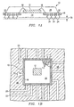
- packaged integrated circuit 10 according to a first preferred embodiment of the invention will now be described in detail. While the following description is provided using the example of a package containing a single integrated circuit chip, it is of course to be understood that the present invention is also applicable to the packaging or mounting of multiple integrated circuit chips to a board, for example in a hybrid integrated circuit or multichip module.
- the active element of packaged integrated circuit 10 is semiconductor chip 12, which is a solid-state integrated circuit device such as a microprocessor, memory, logic device, analog device or other electronic function implemented in a single-chip integrated circuit, as known in the art. According to this embodiment of the invention, chip 12 is attached on its bottom (inactive) surface to conductive slug 14, mounted within and below the plane of substrate 16.
- Substrate 16 may be a ceramic substrate, printed circuit board, or other similar substrate having conductors 17 upon or within the substrate (see Figure 1B) for carrying electrical signals to and from chip 12, and having an opening or receptacle therein within which the conductive slug 14 is mounted.
- Bond wires 18 connect conductors 17 to bond pads on chip 12 in the conventional manner.
- Plated-through vias 22 make connection between conductors 17 on the top surface of substrate 16 and solder balls 24 on the lower surface of substrate 16.
- solder balls 24 are arranged in the conventional ball-grid-array manner around conductive slug 14, and correspond to lands or other surface conductors 23 (see Figure 1B) on the top surface of system circuit board 28 (see Figure 2A) to which packaged integrated circuit 10 is to be mounted.
- Conductive slug 14 is preferably formed of a material with high thermal conductivity, so that heat from chip 12 may be readily conducted therethrough. In addition, if electrical connection is to be made to chip 12, conductive slug 14 is also preferably electrically conductive. The preferred material for conductive slug 14 is believed to be copper, but other materials known in the art to be thermally conductive and, if desired, electrically conductive, may alternatively be used for slug 14.
- Solder balls 24 are also disposed in an array manner beneath and in contact with substrate 16. Slug 14 and solder balls 24 are capable of conducting heat away from chip 12. Slug 14 may be connected to a ground plane within system circuit board 28 (see Figure 2A). The ground plane may be biased to ground or another substrate bias voltage, in which case slug 14 will also provide proper grounding for chip 12. While packaged integrated circuit 10, according to this embodiment of the invention, is shown in Figure 2A as attached to system circuit board 28, it is to be understood by those of ordinary skill in the art that packaged integrated circuit 10 will often be individually manufactured and sold, with the purchaser performing the installation of packaged integrated circuit 10 to system circuit board 28 in a computer or other end equipment.
- packaged integrated circuit 10 begins with the insertion of slug 14 into the corresponding cavity of substrate 16; slug 14 is preferably epoxied into this cavity for mechanical integrity.
- Chip 12 is then mounted to the top surface of slug 14 by conventional die attach techniques, such as a conductive epoxy or eutectic mount.
- Bond wires 18 are then attached between substrate 16 and chip 12 by conventional techniques, such as thermocompression or ultrasonic bonding.
- encapsulant 20 is formed over chip 12 and wires 18 in the conventional manner.
- encapsulate 20 is formed by conventional transfer molding; alternatively, encapsulant 20 may be "globbed" over chip 12 and substrate 16 by dispensation and curing, in the conventional manner.
- Solder balls 24 are formed on the underside of substrate 24, in the conventional manner, for example, by way of a solder mask (not shown) on the underside of substrate 16.
- packaged integrated circuit 10 Upon completion of the construction of packaged integrated circuit 10, and any desired electrical testing in packaged form, packaged integrated circuit 10 is ready for mounting to system circuit board 28 (see Figure 2A). Mounting of packaged integrated circuit 10 is preferably done by way of IR reflow or other conventional technique for the surface mounting of BGA packages to circuit boards.
- conductive slug 14 may be plated on the underside region at interface 29 between the slug 14 and system circuit board 28. Plating slug 14 will create a wettable surface during reflow which will bond to system circuit board 28 maximizing the area of thermal conduction from chip 12 to system circuit board 28. This thermal conduction path will enable system circuit board 28 to behave as a heat sink.
- Conductive slug 14 may be plated with conventional materials such as tin or nickel or other appropriate plating material. Alternatively, due to process variations, during reflow a small air gap or void may remain between slug 14 and system circuit board 28 without substantially impairing the ability of slug 14 to provide a thermal conduction path from chip 12 to system circuit board 28.
- Conductive slug 14 will serve as a stand-off during solder reflow of solder bumps 24.
- the specific collapse distance 26 of the solder bumps is determined by the height of conductive slug 14 below the plane of substrate 16.
- the shape of the solder bumps 24 after reflow will be determined by the starting volume of solder and the collapse distance 26.
- the shape of solder bumps 24 after reflow may remain substantially circular (see Figure 2A) or may result in an hour-glass shape (see Figure 2B).
- the hour-glass shape may be more desirable and may be optimized according to the specific collapse distance 26 and starting volume of solder.
- Figures 3 and 4 illustrate, in cross-section, packaged integrated circuit 30 according to a second embodiment of the invention.
- packaged integrated circuit 30 includes chip 32 mounted upon thermally conductive slug 34.
- Slug 34 lies below the plane of substrate 36 and is attached to the underside of substrate 36 at locations 35 providing a lateral surface of substrate 36 to which slug 34 may be epoxied or otherwise securely fastened.
- an opening is provide through substrate 36, to which chip 32 is mounted.
- This construction allows for a reduced height of the overall package and provides for the maximum area for the arrangement of bond wire lands on substrate 36 with minimum wire length, while maximizing the surface area of thermal conduction on the underside.
- Bond wires 38 electrically connect conductors (not shown) in substrate 36 to pads on the surface of chip 32.
- encapsulant 40 is disposed over the cavity of substrate 36, and thus over chip 32 and wires 38.
- Encapsulant 40 according to this embodiment of the invention, is dispensed by way of a syringe or other liquid dispenser, and is then cured in a conventional manner for so-called "chip-on-board" construction.
- Solder balls 42 are attached to lands on the bottom of substrate 36 around thermally conductive slug 34. Vias (not shown) are provided within substrate 36 to provide electrical connection to the conductors in the substrate. A solder mask (not shown) may be provided on the underside of substrate 36 to aid in defining the location of solder balls 42, during the attachment in the conventional manner.
- packaged integrated circuit 30 is attached to system circuit board 46 (see figure 4) by way of infrared (IR) solder reflow or other conventional surface mount technique.
- Solder balls 42 and slug 34 may connect to a thermal conductor within system circuit board 46, thus providing a path of relatively low thermal resistance between chip 32 and system circuit board 46.
- conductive slug 34 will serve as a stand-off during the solder reflow of solder bumps 42.
- the shape of the solder bumps after reflow will be determined by the volume of solder before reflow and the specific collapse distance 44 (see Figure 3).
- the underside of slug 34 may be plated to create a wettable surface during reflow at the interface 45 between slug 34 and system circuit board 46 to form a strong bond and enhance the thermal conduction from chip 32 to system circuit board 46.
Landscapes
- Engineering & Computer Science (AREA)
- Manufacturing & Machinery (AREA)
- Microelectronics & Electronic Packaging (AREA)
- Cooling Or The Like Of Semiconductors Or Solid State Devices (AREA)
Claims (15)
- Eingehäuste integrierte Schaltung (10, 30), die auf einer Oberseite einer Leiterplatte (28, 46) befestigt ist, wobei die eingehäuste integrierte Schaltung umfasst:dadurch gekennzeichnet, dass eine Unterseite des Blocks die Oberseite der Leiterplatte kontaktiert, undein Substrat (16, 36) mit einer durchgehenden Öffnung und mit mehreren elektrischen Leitern;einen Block (14, 34), der mit dem Substrat verbunden ist und ein wärmeleitendes Material aufweist;einen Chip mit einer integrierten Schaltung (12, 32), der auf einer Oberseite des Blocks, der in der Öffnung des Substrats freiliegt und elektrisch mit den Leitern des Substrats verbunden ist, befestigt ist; undmehrere Lötperlen (24, 32), die mit einer Unterseite des Substrats in elektrischer Verbindung mit den Leitern des Substrats verbunden ist und mit der Leiterplatte durch ein Aufschmelzverfahren verbunden ist,
dass ein Abschnitt der Oberseite des Blocks die Unterseite des Substrats kontaktiert, wobei dadurch ein Abschnitt des Blocks zwischen dem Substrat und der Leiterplatte einen Abstand zwischen der Oberseite der Leiterplatte und der Unterseite des Substrats definiert, wobei der Abstand, der durch den Block bestimmt ist, einen Kollapsabstand für die Lötperlen während des Aufschmelzens bestimmt, wodurch eine effektive Wärmeleitung durch den Block zwischen dem Chip und der Leiterplatte zur Verfügung gestellt wird. - Eingehäuste integrierte Schaltung nach Anspruch 1, wobei die Oberseite des Blocks (14, 32) eine erste und eine zweite Ebene aufweist, wobei ein Abschnitt des Blocks sich durch die Öffnung erstreckt, wobei die zweite Ebene der Oberseite des Blocks im Wesentlichen eben zu der zweiten Oberseite des Substrats (16, 36) ist.
- Eingehäuste integrierte Schaltung nach Anspruch 1, die weiterhin umfasst:ein Einkapselungsmittel (20, 40), das auf dem Chip mit der integrierten Schaltung (12, 32), auf einem Abschnitt der zweiten Oberfläche des Substrats und auf einem Abschnitt der Oberseite des Blocks aufgebracht ist.
- Eingehäuste integrierte Schaltung nach Anspruch 3, wobei das Einkapselungsmittel einen spritzgußfähigen Kunststoff umfasst.
- Eingehäuste integrierte Schaltung nach Anspruch 1, wobei das Substrat entweder eine Leiterplatte oder ein Keramiksubstrat umfasst.
- Eingehäuste integrierte Schaltung nach Anspruch 1, wobei der Block Kupfer enthält.
- Eingehäuste integrierte Schaltung nach Anspruch 1, wobei die veränderte Form jedes der mehreren Lötperlen nach dem Aufschmelzen entweder im Wesentlichen rund oder im wesentlichen sanduhrförmig ist.
- Eingehäuste integrierte Schaltung nach Anspruch 1, die weiterhin umfasst:einen metallisierten Bereich der ersten Oberfläche des leitenden Blockes.
- Verfahren zum Befestigen einer eingehäusten integrierten Schaltung (10, 30) auf einer Oberseite einer Leiterplatte (28, 46), mit folgenden Schritten:wobei die eingehäuste integrierte Schaltung (10, 30), den wärmeleitenden Block, das Substrat, den Chip mit der integrierten Schaltung und die Lötperlen umfasst;Anordnen eines wärmeleitenden Blockes (14, 34) auf einem Substrat (16, 36), wobei das Substrat eine durchgehende Öffnung und mehrere elektrische Leiter aufweist;Befestigen eines Chips (12, 32) mit einer integrierten Schaltung auf einer Oberseite des Blocks, der in der Öffnung in dem Substrat freiliegt und elektrisch den Chip mit der integrierten Schaltung mit den mehreren elektrischen Leitern verbindet;Einkapseln des Chips mit der integrierten Schaltung;Anordnen von mehreren Lötperlen (24, 42) auf eine Unterseite des Substrats in elektrischer Verbindung mit den Leitern des Substrats;
Anordnen der eingehäusten integrierten Schaltung auf einer Oberseite der Leiterplatte;
dadurch gekennzeichnet, dass das Verfahren die weiteren Schritte umfasst:Verbinden des leitenden Blockes mit der Unterseite des Substrats, wobei eine Unterseite des Blocks unter der Ebene der Unterseite des Substrats liegt; undDurchführen eines Aufschmelzverfahrens, so dass die Unterseite des wärmeleitenden Blocks (14, 34) die Oberseite der Leiterplatte kontaktiert, und so dass ein Abschnitt der Oberseite des Blocks die Unterseite des Substrats kontaktiert, wodurch ein Abschnitt des Blocks zwischen dem Substrat und der Leiterplatte einen Abstand zwischen der Oberseite der Leiterplatte und der Unterseite des Substrats definiert, wobei der Abstand, der durch den Block bestimmt ist, einen Kollapsabstand für die Lötperlen während des Aufschmelzens bestimmt, wodurch eine effektive Wärmeleitung durch den Block zwischen dem Chip und der Leiterplatte zur Verfügung gestellt wird. - Verfahren nach Anspruch 9, wobei die Oberseite des wärmeleitenden Blocks (14, 34) eine erste und eine zweite Ebene umfasst, wobei der Schritt des Befestigen des wärmeleitenden Blockes an der Oberseite des Substrats (16, 36) weiterhin den Schritt umfasst:Einfügen des wärmeleitenden Blockes in das Substrat, wobei die erste Ebene der Oberseite mit der ersten Oberfläche des Substrats verbunden ist und wobei die zweite Ebene der Oberseite im Wesentlichen eben zu der zweiten Oberfläche des Substrats ist.
- Verfahren nach Anspruch 9, wobei der Schritt des Einkapselns weiterhin umfasst:Spritzgießen einer Kunststoffverbindung über den Chip mit der integrierten Schaltung.
- Verfahren nach Anspruch 9, wobei der Schritt des Einkapselns weiterhin die Schritte umfasst:Aufbringen eines Kunststoffs auf den Chip mit der integrierten Schaltung; undAusheilen des aufgebrachten Kunststoffs.
- Verfahren nach Anspruch 9, das weiterhin den Schritt umfasst:Metallisieren der Unterseite des wärmeleitenden Blocks.
- Verfahren nach Anspruch 9, das weiterhin den Schritt umfasst:Verbinden von mehreren Drahtverbindungen (18, 38) mit einer Oberseite des Chips mit der integrierten Schaltung und der Oberseite des Substrats.
- Verfahren nach Anspruch 14, wobei der Schritt des Verbindens entweder ein Ultraschallverbinden oder ein Thermokompressionsverbinden umfasst.
Applications Claiming Priority (2)
| Application Number | Priority Date | Filing Date | Title |
|---|---|---|---|
| US225138 | 1994-04-08 | ||
| US08/225,138 US5991156A (en) | 1993-12-20 | 1994-04-08 | Ball grid array integrated circuit package with high thermal conductivity |
Publications (3)
| Publication Number | Publication Date |
|---|---|
| EP0676806A2 EP0676806A2 (de) | 1995-10-11 |
| EP0676806A3 EP0676806A3 (de) | 1996-02-14 |
| EP0676806B1 true EP0676806B1 (de) | 2004-08-18 |
Family
ID=22843694
Family Applications (1)
| Application Number | Title | Priority Date | Filing Date |
|---|---|---|---|
| EP94309423A Expired - Lifetime EP0676806B1 (de) | 1994-04-08 | 1994-12-16 | Verpackung eines BGA-integrierten Schaltkreises mit hoher thermischer Leitfähigkeit |
Country Status (3)
| Country | Link |
|---|---|
| EP (1) | EP0676806B1 (de) |
| JP (1) | JP3618393B2 (de) |
| DE (1) | DE69433952T2 (de) |
Families Citing this family (5)
| Publication number | Priority date | Publication date | Assignee | Title |
|---|---|---|---|---|
| US5852870A (en) | 1996-04-24 | 1998-12-29 | Amkor Technology, Inc. | Method of making grid array assembly |
| SG63803A1 (en) | 1997-01-23 | 1999-03-30 | Toray Industries | Epoxy-resin composition to seal semiconductors and resin-sealed semiconductor device |
| KR100456482B1 (ko) * | 1997-12-29 | 2005-01-17 | 삼성전자주식회사 | 패터닝된 리드 프레임을 이용한 볼 그리드 어레이 패키지 |
| WO2011036840A1 (ja) * | 2009-09-24 | 2011-03-31 | パナソニック株式会社 | 半導体装置、半導体実装体、および半導体装置の製造方法 |
| JP2015176971A (ja) * | 2014-03-14 | 2015-10-05 | 三菱電機株式会社 | 半導体パッケージ、およびその製造方法 |
Family Cites Families (3)
| Publication number | Priority date | Publication date | Assignee | Title |
|---|---|---|---|---|
| US4922324A (en) * | 1987-01-20 | 1990-05-01 | Kabushiki Kaisha Toshiba | Semiconductor integrated circuit device |
| US5157480A (en) * | 1991-02-06 | 1992-10-20 | Motorola, Inc. | Semiconductor device having dual electrical contact sites |
| US5285352A (en) * | 1992-07-15 | 1994-02-08 | Motorola, Inc. | Pad array semiconductor device with thermal conductor and process for making the same |
-
1994
- 1994-12-16 DE DE69433952T patent/DE69433952T2/de not_active Expired - Lifetime
- 1994-12-16 EP EP94309423A patent/EP0676806B1/de not_active Expired - Lifetime
-
1995
- 1995-04-10 JP JP08360695A patent/JP3618393B2/ja not_active Expired - Lifetime
Also Published As
| Publication number | Publication date |
|---|---|
| JP3618393B2 (ja) | 2005-02-09 |
| EP0676806A2 (de) | 1995-10-11 |
| EP0676806A3 (de) | 1996-02-14 |
| JPH07297311A (ja) | 1995-11-10 |
| DE69433952T2 (de) | 2005-01-05 |
| DE69433952D1 (de) | 2004-09-23 |
Similar Documents
| Publication | Publication Date | Title |
|---|---|---|
| US5991156A (en) | Ball grid array integrated circuit package with high thermal conductivity | |
| EP0690500B1 (de) | Kugelmatrixgehäuse für integrierte Schaltung mit lötverbundenen thermischen Leiter | |
| US5977626A (en) | Thermally and electrically enhanced PBGA package | |
| US5541450A (en) | Low-profile ball-grid array semiconductor package | |
| JP4476482B2 (ja) | ロープロファイルボールグリッドアレイ半導体パッケージ、集積回路、印刷回路板、プロセサシステム、ロープロファイルボールグリッドアレイ半導体パッケージを製造する方法、および、半導体ダイを搭載する方法 | |
| US6031284A (en) | Package body and semiconductor chip package using same | |
| KR100694739B1 (ko) | 다수의 전원/접지면을 갖는 볼 그리드 어레이 패키지 | |
| US5583377A (en) | Pad array semiconductor device having a heat sink with die receiving cavity | |
| US5903052A (en) | Structure for semiconductor package for improving the efficiency of spreading heat | |
| US7145225B2 (en) | Interposer configured to reduce the profiles of semiconductor device assemblies and packages including the same and methods | |
| US6492726B1 (en) | Chip scale packaging with multi-layer flip chip arrangement and ball grid array interconnection | |
| US5834839A (en) | Preserving clearance between encapsulant and PCB for cavity-down single-tier package assembly | |
| US20020195699A1 (en) | Packaged die on PCB with heat sink encapsulant | |
| US20040164404A1 (en) | Semiconductor package with heat dissipating structure | |
| US6894229B1 (en) | Mechanically enhanced package and method of making same | |
| JPH09153565A (ja) | ヒートシンク付きボールグリッドアレーパッケージ | |
| US20020031865A1 (en) | Method for fabricating a dual-chip package and package formed | |
| US20100019374A1 (en) | Ball grid array package | |
| US7344916B2 (en) | Package for a semiconductor device | |
| US10068841B2 (en) | Apparatus and methods for multi-die packaging | |
| KR100995478B1 (ko) | 패키지형 반도체 디바이스 및 그 형성 방법 | |
| JP3148718B2 (ja) | 熱的及び電気的に増強された半導体パッケージ | |
| EP0676806B1 (de) | Verpackung eines BGA-integrierten Schaltkreises mit hoher thermischer Leitfähigkeit | |
| US6248951B1 (en) | Dielectric decal for a substrate of an integrated circuit package | |
| KR100230189B1 (ko) | 볼 그리드 어레이 반도체 패키지 |
Legal Events
| Date | Code | Title | Description |
|---|---|---|---|
| PUAI | Public reference made under article 153(3) epc to a published international application that has entered the european phase |
Free format text: ORIGINAL CODE: 0009012 |
|
| AK | Designated contracting states |
Kind code of ref document: A2 Designated state(s): DE FR GB IT |
|
| PUAL | Search report despatched |
Free format text: ORIGINAL CODE: 0009013 |
|
| AK | Designated contracting states |
Kind code of ref document: A3 Designated state(s): DE FR GB IT |
|
| 17P | Request for examination filed |
Effective date: 19960803 |
|
| 17Q | First examination report despatched |
Effective date: 19971105 |
|
| RAP3 | Party data changed (applicant data changed or rights of an application transferred) |
Owner name: STMICROELECTRONICS, INC. |
|
| APAB | Appeal dossier modified |
Free format text: ORIGINAL CODE: EPIDOS NOAPE |
|
| APAB | Appeal dossier modified |
Free format text: ORIGINAL CODE: EPIDOS NOAPE |
|
| APAB | Appeal dossier modified |
Free format text: ORIGINAL CODE: EPIDOS NOAPE |
|
| APAD | Appeal reference recorded |
Free format text: ORIGINAL CODE: EPIDOS REFNE |
|
| APBZ | Receipt of observations in appeal recorded |
Free format text: ORIGINAL CODE: EPIDOSNOBA4E |
|
| APBT | Appeal procedure closed |
Free format text: ORIGINAL CODE: EPIDOSNNOA9E |
|
| GRAP | Despatch of communication of intention to grant a patent |
Free format text: ORIGINAL CODE: EPIDOSNIGR1 |
|
| GRAS | Grant fee paid |
Free format text: ORIGINAL CODE: EPIDOSNIGR3 |
|
| GRAA | (expected) grant |
Free format text: ORIGINAL CODE: 0009210 |
|
| AK | Designated contracting states |
Kind code of ref document: B1 Designated state(s): DE FR GB IT |
|
| PG25 | Lapsed in a contracting state [announced via postgrant information from national office to epo] |
Ref country code: IT Free format text: LAPSE BECAUSE OF FAILURE TO SUBMIT A TRANSLATION OF THE DESCRIPTION OR TO PAY THE FEE WITHIN THE PRE;WARNING: LAPSES OF ITALIAN PATENTS WITH EFFECTIVE DATE BEFORE 2007 MAY HAVE OCCURRED AT ANY TIME BEFORE 2007. THE CORRECT EFFECTIVE DATE MAY BE DIFFERENT FROM THE ONE RECORDED.SCRIBED TIME-LIMIT Effective date: 20040818 |
|
| REG | Reference to a national code |
Ref country code: GB Ref legal event code: FG4D |
|
| REF | Corresponds to: |
Ref document number: 69433952 Country of ref document: DE Date of ref document: 20040923 Kind code of ref document: P |
|
| ET | Fr: translation filed | ||
| PLBE | No opposition filed within time limit |
Free format text: ORIGINAL CODE: 0009261 |
|
| STAA | Information on the status of an ep patent application or granted ep patent |
Free format text: STATUS: NO OPPOSITION FILED WITHIN TIME LIMIT |
|
| 26N | No opposition filed |
Effective date: 20050519 |
|
| APAH | Appeal reference modified |
Free format text: ORIGINAL CODE: EPIDOSCREFNO |
|
| PGFP | Annual fee paid to national office [announced via postgrant information from national office to epo] |
Ref country code: GB Payment date: 20131125 Year of fee payment: 20 Ref country code: DE Payment date: 20131121 Year of fee payment: 20 |
|
| PGFP | Annual fee paid to national office [announced via postgrant information from national office to epo] |
Ref country code: FR Payment date: 20131219 Year of fee payment: 20 |
|
| REG | Reference to a national code |
Ref country code: DE Ref legal event code: R071 Ref document number: 69433952 Country of ref document: DE |
|
| REG | Reference to a national code |
Ref country code: GB Ref legal event code: PE20 Expiry date: 20141215 |
|
| PG25 | Lapsed in a contracting state [announced via postgrant information from national office to epo] |
Ref country code: GB Free format text: LAPSE BECAUSE OF EXPIRATION OF PROTECTION Effective date: 20141215 |