EP0676855B1 - Versorgung-unterscheidendes und Versorgung-adaptierendes elektronisches System - Google Patents
Versorgung-unterscheidendes und Versorgung-adaptierendes elektronisches System Download PDFInfo
- Publication number
- EP0676855B1 EP0676855B1 EP95104833A EP95104833A EP0676855B1 EP 0676855 B1 EP0676855 B1 EP 0676855B1 EP 95104833 A EP95104833 A EP 95104833A EP 95104833 A EP95104833 A EP 95104833A EP 0676855 B1 EP0676855 B1 EP 0676855B1
- Authority
- EP
- European Patent Office
- Prior art keywords
- voltage
- supply
- supply voltage
- reset
- circuit
- Prior art date
- Legal status (The legal status is an assumption and is not a legal conclusion. Google has not performed a legal analysis and makes no representation as to the accuracy of the status listed.)
- Expired - Lifetime
Links
- 238000000034 method Methods 0.000 claims description 8
- 230000000630 rising effect Effects 0.000 claims 3
- 238000010586 diagram Methods 0.000 description 10
- 238000001514 detection method Methods 0.000 description 8
- 230000001105 regulatory effect Effects 0.000 description 6
- 230000006978 adaptation Effects 0.000 description 1
- 230000006399 behavior Effects 0.000 description 1
- 230000001934 delay Effects 0.000 description 1
- 230000001419 dependent effect Effects 0.000 description 1
- 230000036039 immunity Effects 0.000 description 1
- 239000004065 semiconductor Substances 0.000 description 1
- 239000007858 starting material Substances 0.000 description 1
Images



Classifications
-
- H—ELECTRICITY
- H02—GENERATION; CONVERSION OR DISTRIBUTION OF ELECTRIC POWER
- H02M—APPARATUS FOR CONVERSION BETWEEN AC AND AC, BETWEEN AC AND DC, OR BETWEEN DC AND DC, AND FOR USE WITH MAINS OR SIMILAR POWER SUPPLY SYSTEMS; CONVERSION OF DC OR AC INPUT POWER INTO SURGE OUTPUT POWER; CONTROL OR REGULATION THEREOF
- H02M3/00—Conversion of DC power input into DC power output
- H02M3/02—Conversion of DC power input into DC power output without intermediate conversion into AC
- H02M3/04—Conversion of DC power input into DC power output without intermediate conversion into AC by static converters
- H02M3/06—Conversion of DC power input into DC power output without intermediate conversion into AC by static converters using resistors or capacitors, e.g. potential divider
- H02M3/07—Conversion of DC power input into DC power output without intermediate conversion into AC by static converters using resistors or capacitors, e.g. potential divider using capacitors charged and discharged alternately by semiconductor devices with control electrode, e.g. charge pumps
-
- Y—GENERAL TAGGING OF NEW TECHNOLOGICAL DEVELOPMENTS; GENERAL TAGGING OF CROSS-SECTIONAL TECHNOLOGIES SPANNING OVER SEVERAL SECTIONS OF THE IPC; TECHNICAL SUBJECTS COVERED BY FORMER USPC CROSS-REFERENCE ART COLLECTIONS [XRACs] AND DIGESTS
- Y10—TECHNICAL SUBJECTS COVERED BY FORMER USPC
- Y10S—TECHNICAL SUBJECTS COVERED BY FORMER USPC CROSS-REFERENCE ART COLLECTIONS [XRACs] AND DIGESTS
- Y10S323/00—Electricity: power supply or regulation systems
- Y10S323/901—Starting circuits
Definitions
- the present invention relates to electronic systems with supply-adaptive reference generation and more specifically to supplying and regulating external devices such as PCMCIA cards from the supply of a personal computer.
- PCMCIA-compatible cards which may be functional at 3.3 volt but plugged into a 5-volt system such as a laptop computer. Detection and adaptation by the PCMCIA card thus become an integral part of the power-on process. Without the procedure prior to power-on, the PCMCIA card may be operating under an incompatible supply and system configuration.
- a voltage regulator and voltage doubler are implemented with the IA circuit.
- the voltage regulator and voltage doubler generate a DC voltage of 5 volt regardless of the system power supply being 5 volt or 3.3 volt.
- This approach allows the 5-volt components of a system, such as a PCMCIA card for a notebook computer to be functional with both 5-volt and 3.3-volt supplies without the need to redesign the existing components.
- the conventional approach requires the system to generate an accurate reference voltage for the voltage regulator and voltage doubler so that the voltage generated thereafter is as close to 5 volt as possible.
- this bandgap reference voltage in many cases may only be operational under a 5-volt steady supply. Since the voltage regulator and voltage doubler also require an accurate reference voltage to generate a DC voltage of about 5 volt for invoking the bandgap voltage, the voltage regulator and voltage doubler cannot use the bandgap reference voltage as their reference voltage during system power-up transients.
- US-A-5,073,850 which relates to a power supply control integrated circuit that includes an internal start circuit.
- the start circuit monitors the time that an output of a latch is in a first logic state such that after a predetermined length of time has elapsed the start circuit forces a second logic state to occur at the output of the latch.
- EP-A-0 470 498 discloses a voltage reference initialization circuit for a voltage reference generator.
- the initialization circuit has a starter circuit connected to the input of the voltage reference generator and to an external voltage supply to initially couple the input of the reference generator to the external voltage supply and thereby start the reference generator. It also has a pump circuit.
- the pump circuit is connected to the input of the voltage reference generator and to the external voltage supply. It is coupled to the output of the reference generator.
- the pump circuit pumps a fixed charge from the external voltage supply into the voltage reference generator.
- Such a circuit may be incorporated into a semiconductor memory device having an on chip voltage reference generator.
- a circuit for detecting the level of a supply voltage as set forth in claim 1 and a method of supply discriminating for an integrated circuit as set forth in claim 5 is provided. Preferred embodiments are disclosed in the dependent claims.
- a novel supply discriminator circuit for detecting the level of a supply voltage during power-up of a system for configuring an IA circuit such as a PCMCIA card coupled to the system.
- the circuit compares a reference voltage with a divided-down supply voltage and latches the result after a predetermined delay. The delay thus provides timing for the reference voltage to stabilize after power-up to assure accurate detection, as well as noise immunity from other devices.
- FIG. 1 illustrates a functional block diagram of a supply-adaptive voltage generation circuit in accordance with the present invention.
- FIG. 2 illustrates a circuit diagram of the reference generator for the diode reference, bandgap reference and sleep mode reference as incorporated in the present invention.
- FIG. 3 illustrates a timing diagram for the supply-adaptive internal voltage generation circuit.
- FIG. 4 illustrates a novel DC-DC power supply converter incorporated in the present invention.
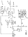
- FIG. 5 illustrates a circuit diagram of a novel supply-adaptive VCC detection circuit incorporated in the present invention.
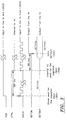
- FIG. 6 illustrates the timing behavior of the supply-adaptive detection circuit.
- FIG. 7 illustrates the circuit diagram of another embodiment of the reference generation circuit for the voltage regulator shown in FIG. 1.
- Modem VCC 100 for the IA can be either 3.3 volt or 5 volt as supplied by a system such as a notebook computer.
- Modem VCC 100 is applied to a voltage regulator, which is formed by p-channel transistor 115, amplifier 120 and resistors R1 and R2.
- Voltage doubler 135 is coupled to the output of the voltage regulator at node 116.
- the operation of voltage doubler 135 is driven by clock 130. Currently the clock rate is set at 125 KHz.
- Output node 136 of voltage doubler 135 is connected to IA VCC node 151 through switch 150.
- modem VCC 100 represents the 3.3V or 5V which are supplied by a system such as a personal computer
- IA VCC 151 represents the 5 volt VCC operating an IA circuit such as a PCMCIA card.
- Bypass path 105 connects between modem VCC 100 and switch 150.
- the output of switch 150 is applied to IA VCC 151 at 5 volt for the IA circuit.
- Supply-adaptive ("SA") VCC detection circuit 140 is connected to bypass path 105 and generates a control signal 141 (5 volt or 3 volt) for switch 150 to control switching.
- Reference generation circuit 161 has three modes: diode reference 160, IA bandgap reference 170 and sleep mode reference 180. Start-up timer 190 facilitates the necessary switching among the three reference voltages.
- Bandgap reference 170 can also be used for the IA circuit as IA reference 171.
- a diode-connected N-channel transistor 110 is connected between modem VCC 100 and node 136 for providing an initial voltage drop at node 136 when modem VCC 100 is first powered up.
- diode reference voltage 160 which currently is a forward-biased diode-connected PNP transistor (to be described in Fig. 2), provides the requisite reference voltage for amplifier 120 of the voltage regulator. Node 116 is thus regulated at about 2.75 volt, without regard to whether modem VCC 100 is a 3.3 volt or 5 volt supply.
- the voltage at node 116 is multiplied by voltage doubler 135 to about 5 volt at node 136, which is sufficient to activate the bandgap voltage of the IA device such that IA bandgap voltage 170 can now be used as a more precise voltage reference for the regulator's amplifier 120 after a predetermined time delay for modem VCC 100 to settle.
- a timing diagram is shown in Figure 3, where diode reference 160 is first used as input to the regulator upon power-on reset (POR) and IA bandgap reference 170 is used after the 180 ms delay, as currently implemented.
- switch 150 is used to switch IA VCC 151 to modem VCC 100 through bypass 105 when modem VCC 100 is 5 volt as detected by SA VCC detector 140. This feature is advantageous in that once a 5 volt modem VCC is detected, it can readily supply the 5 volt to IA VCC 151 without the redundancy of operating the regulator and doubler circuitry.
- IA bandgap voltage 170 is generally more precise as reference voltage than forward-biased diode 160 such that once IA bandgap voltage 170 is activated, diode reference voltage 160 can be de-activated to reduce power consumption.
- “Sleep” mode reference voltage 180 generates the reference voltage for amplifier 120 of the regulator when the IA circuit is reviving from sleep mode, i.e. when the IA circuit is not used by the system for an extended period of time.
- sleep mode is different from the power-up situation because the voltage level supplied by modem VCC 100 is already known and detected prior to sleep mode.
- sleep mode reference voltage 180 preserves the information on the level of the supply voltage so that the IA circuit need not go through the delay again in determining modem VCC 100 when it is awakening from sleep mode.
- the operation of sleep mode 180, as well as diode and bandgap references 160, 170, will be described in connection with Figure 2.
- FIG. 2 a circuit diagram of reference generator 161 ( Figure 1) for diode reference 160, bandgap reference 170 and sleep mode reference 180 is further illustrated.
- n-channel transistors 210, 220 and 241 control the switching among the three modes of reference voltages: diode reference voltage 200, bandgap reference voltage node 240 and sleep mode reference voltage node 254.
- Transistor 210 is turned on by CTRL3V 242.
- Diode-connected PNP transistor 200, resistor 231 and p-channel transistor 230 form the connection when the reference is generated by the diode reference voltage 160 of Figure 1.
- the bandgap reference voltage 170 (Figure 1) is available at node 20 when both transistors 220, 241 are turned on and transistor 210 is turned off. Sleep mode can be activated when transistor 241 is turned off to cut off the voltage at node 240 from node 254. Also, transistors 255, 256, 257 are turned on when sleep mode is activated. Also during sleep mode, transistors 258 and 259 are turned off to break the d.c. path to save power.
- timer 25 When coming out of sleep mode, timer 25 opens a switch at transistor 257 by turning it off so that the voltage level at node 254 is boosted until node 254 is stabilized. Timer 25 and transistors 255 and 256 are then turned off and transistor 241 is turned on to go back into normal operation.
- transistors 200, 210, 230 and resistor 231 are turned on to provide the reference voltage at node 20.
- This voltage at node 20 can be used as a reference voltage for regulator 120 in Figure 1 as Vref.
- IAVcc Figure 1
- the voltage level at node 240 reaches about 1.25 volt.
- transistors 210 and 230 are turned off while transistors 220 and 241 are turned on to provide the 1.25 volt at node 240 to node 220 so that it can be used as the regulator (120, Fig. 1) input at node 20.
- transistors 251 and 255 are turned off.
- transistors 255, 256 and 257 are turned on and transistors 241, 258, and 259 are turned off. As described above, transistors 258 and 259 are turned off to break the d.c. path to conserve power during the sleep mode.
- resistor divider formed by resistors 251 and 252 provides about 1.25 volt at node 120 to be used as the regulator input.
- the voltage level is preserved during sleep mode when the supply voltage is already detected at 3.3 volts. If the supply voltage is detected at 5 volts, then no information would need to be kept, because the system can readily use the supply voltage as it awakens in a 5 volt condition. In this case, the voltage regulator and multiplier can thus be disabled during sleep mode for the 5 volt condition detected.
- timer 25 When coming out of sleep mode, timer 25 would delay the turning off of transistors 255 and 256 until the voltage level at node 240 is about 1.25 volts. Transistors 258 and 259 are also turned on. Transistor 257 is also turned off to provide more boost to the system that is coming out of sleep mode. When voltage at node 240 is settled, timer 25 goes on to turn off transistor 255 and 256 and to turn on transistor 241.
- FIG. 3 a timing diagram for the supply-adaptive IA voltage generation is illustrated. Note that the diode reference is first used at 300 as an input to the regulator. A predetermined delay later, the band-gap reference voltage is activated and can be used as an input to the regulator at 310. Another time delay later, currently set at 80 ms, a valid detection of the modem VCC is made with the DETCK going high.
- Supply voltage 400 is first used to generate a voltage drop across diode-connected n-channel transistor 401 at node 420 for providing the start-up conditions.
- Supply voltage 400 is then regulated by regulator 403 formed by transistor 404 and amplifier 402.
- voltage doubler 440 doubles it to generate a supply for the IA circuit at node 420, which is equal to two times Vcc at node 410.
- the IA supply voltage can be made a real-number multiple of supply voltage 400 by using voltage drop 401 and doubler 440.
- Switches, as illustrated in Fig. 4 act to provide the phases 1 and 2 needed for doubling the voltage from node 410 to node 420.
- Switches as illustrated in Fig. 4 act to provide the phases 1 and 2 needed for doubling the voltage from node 410 to node 420.
- FIG. 5 a circuit diagram of a novel supply-adaptive Vcc detect circuit 140 ( Figure 1) incorporated in the present invention is illustrated.
- the inverting input to comparator 510 is reference generator 500, which may come from a temperature-regulated supply-insensitive reference generator.
- the non-inverting input to comparator 510 is a resistor divider for Vcc 501, which is either 3.3 volt or 5 volt.
- the output of comparator 510 is applied to latch 520, which is clocked by DETCK 532 from timer 530.
- DETCK 532 is also used to reset other components during power-on.
- Timer 530 is reset by power-on reset (POR) 531 when the system supply voltage is first turned on.
- POR power-on reset
- timer 530 holds DETCK 532 low for a predetermined time, ensuring that all devices are to be held in reset state upon power-on.
- Comparator 510 then compares the divided-down Vcc 501 with a voltage generated by Vref 500. If Vcc 501 is 5 volt, comparator 510 output is high and a "1" is latched. If Vcc 501 is 3.3 volt, a "0" is latched. At the end of the time delay, DETOUT 521 is thus a valid indication of Vcc 510, and DETCK 532 goes high allowing all other devices to come out of reset with configuration consistent with Vcc 501.
- FIG. 7 where another embodiment of reference generation circuit for the voltage regulator shown in Figure 1 is illustrated.
- This reference voltage generation circuit is capable of providing a bandgap reference voltage operational across the entire voltage range of the system supply voltage, i.e. from 3 volt to about 5.25 volt.
- the biasing scheme including level-shifting, as shown, is necessary for low-voltage operation, which may be below 3.0 volt.
- the biasing scheme works down to as low as: Vgs(p-channel) + V(diode) + 3 Vdsats, or approximately 2.5-plus volt.
- p-channel transistor 710 is biased by p-channel transistors 715, 719.
- P-channel transistor 711 is biased by transistors 716, 718.
- N-channel transistor 713 is biased by n-channel transistor 717 and node 720.
- node 720 is derived from level-shifting the voltage at node P by transistors 727, 728 successively. The net result is that current paths 1, 2, and 3 experience identical currents and Vref is equal to the diode voltages at transistors 710, 711, 713 plus (I times R).
Landscapes
- Engineering & Computer Science (AREA)
- Power Engineering (AREA)
- Power Sources (AREA)
- Control Of Electrical Variables (AREA)
- Continuous-Control Power Sources That Use Transistors (AREA)
Claims (7)
- Eine Schaltung zum Detektieren des Pegels einer Versorgungsspannung (501) von einem System während der "Leistung-ein"-Rückstellung (531) des Systems zur Konfigurierung einer mit dem System gekoppelten integrierten Vorrichtung, wobei die Versorgungsspannung (501) einen von zwei Spannungspegeln besitzt, und wobei folgendes vorgesehen ist:Bezugsgeneratormittel (500) gekoppelt mit der erwähnten integrierten Vorrichtung zur Erzeugung einer Bezugsspannung ansprechend auf die erwähnten Versorgungsspannungs-(501)-ein-Anstieg auf einen vorbestimmten Pegel während der Leistung-ein-Rückstellung-531 des Systems;einen Widerstandsteiler zur Teilung der Versorgungsspannung (501) in eine erste Spannung basierend auf einem vorbestimmten Teilungsfaktor;einen Komperator (510) zum Vergleichen der ersten Spannung mit der Bezugsspannung zur Erzeugung eines Ausgangssignals basierend auf dem Vergleichsergebnis;eine Zeitsteuerung (530) zur Erzeugung eines Clock- oder Taktsignals (532) nach einer vorbestimmten Verzögerung von der Leistung-ein-Rückstellung (531), wobei die Verzögerung hinreichend Zeit dafür vorsieht, daß sich die Versorgungsspannung (501) stabilisiert und ihr Endniveau oder ihren Endpegel erreicht;Verriegelungsmittel (520) zum Verriegeln des Ausgangssignals des Komperators (510) ansprechend auf das Taktsignal (532) von der Zeitsteuerung (530) derart, daß das Ausgangssignal (521) reflektiert welchen der zwei erwähnten Spannungspegel die Versorgungsspannung (501) besitzt.
- Schaltung nach Anspruch 1, wobei das Taktsignal (532) von der Zeitsteuerung (530) auch andere Komponenten des Systems und die erwähnte integrierte Vorrichtung aktiviert, die während der Leistung-ein-Rückstellung (531) des Systems rückgestellt oder rückgesetzt waren.
- Schaltung nach Anspruch 1 oder 2, wobei die Bezugsspannung aus einer Bandabstandsspannung der integrierten Vorrichtung abgeleitet wird, und wobei die Bandabstandsspannung dann aktiviert wird, wenn die Versorgungsspannung (501) den vorbestimmten Pegel erreicht.
- Schaltung nach Anspruch 1 oder 2, wobei die erwähnte Leistung-ein-Rückstellung (531) durch ein Leistung-Ein-Rückstellsignal initiiert wird, wobei die integrierte Vorrichtung eine Bandabstandsspannung besitzt, und zwar im Betrieb befindlich bei einer vorbestimmten Spannung der Versorgungsspannung, wobei die Verriegelung (520) eine D-Typ-Verriegelung ist und die Verriegelungsausgangsgröße der D-Typ-Verriegelung somit repräsentiert auf welchem der zwei Pegel die Versorgungsspannung (501) sich befindet, wobei die Schaltung ferner folgendes aufweist:
Bezugsgeneratormittel (500) gekoppelt mit der integrierten Vorrichtung zur Erzeugung einer Bezugsspannung durch die Bandabstandsspannung aktiviert durch die Versorgungsspannung (501) welche auf den erwähnten vorbestimmten Pegel während der Leistung-ein-Rückstellung (531) ansteigt. - Verfahren zur Versorgungsdiskriminierung einer integrierten Schaltung gekoppelt mit einem elektronischen System zum Detektieren eines Pegels einer Versorgungsspannung (501) aus dem elektronischen System wenn das elektronische System zuerst Leistung-ein-rückgestellt oder rückgesetzt (531) wird, wobei die Versorgungsspannung (501) einen von zwei Pegeln besitzt, und wobei ferner die folgenden Schritte vorgesehen sind:
Die integrierte Schaltung liefert eine Bezugsspannung mit einem Bezugsgenerator (500) ansprechend auf den Anstieg der Versorgungsspannung (501) auf einen vorbestimmten Pegel während der Leistung-ein-Rückstellung oder-Rücksetzung (531) des elektronischen Systems;Herunterteilen der Versorgungsspannung (501) auf eine erste Spannung mit einem Widerstandsteiler basierend auf einem vorbestimmten Divisionsfaktor;Vergleichen der erwähnten ersten Spannung mit der Bezugsspannung unter Verwendung eines Komperators (510) und Erzeugung eines Ausgangssignals, welches das Vergleichsergebnis repräsentiert;Erzeugung eines Clock- oder Taktsignals (530) nach einer vorbestimmten Verzögerung aus der Leistung-ein-Rückstellung (531), um zu gestatten, daß sich die Versorgungsspannung (501) stabilisiert und ihren Endpegel erreicht;Verriegeln des Ausgangssignals von dem Komperator (510), dann wenn das Taktsignal (532) erzeugt wird, derart, daß das erwähnte Ausgangssignal (521) reflektiert welcher welchen der zwei Spannungspegel die Versorgungsspannung (501) besitzt. - Verfahren nach Anspruch 5, wobei die Bezugsspannung aus einer Bandabstandsspannung von der integrierten Schaltung abgeleitet wird, wobei die Bandabstandsspannung aktiviert wird wenn die Versorgungsspannung (501) vom elektronischen System den vorbestimmten Pegel erreicht.
- Verfahren nach Anspruch 5 oder 6, wobei das Taktsignal (532) von der Zeitsteuerung (530) auch andere Komponenten des elektronischen Systems und die integrierte Vorrichtung aktiviert.
Applications Claiming Priority (2)
| Application Number | Priority Date | Filing Date | Title |
|---|---|---|---|
| US08/226,198 US5514951A (en) | 1994-04-11 | 1994-04-11 | Supply-discriminating supply-adaptive electronic system |
| US226198 | 1994-04-11 |
Publications (3)
| Publication Number | Publication Date |
|---|---|
| EP0676855A2 EP0676855A2 (de) | 1995-10-11 |
| EP0676855A3 EP0676855A3 (de) | 1996-09-04 |
| EP0676855B1 true EP0676855B1 (de) | 2000-09-06 |
Family
ID=22847972
Family Applications (1)
| Application Number | Title | Priority Date | Filing Date |
|---|---|---|---|
| EP95104833A Expired - Lifetime EP0676855B1 (de) | 1994-04-11 | 1995-03-31 | Versorgung-unterscheidendes und Versorgung-adaptierendes elektronisches System |
Country Status (4)
| Country | Link |
|---|---|
| US (1) | US5514951A (de) |
| EP (1) | EP0676855B1 (de) |
| JP (1) | JPH07325638A (de) |
| DE (1) | DE69518687T2 (de) |
Families Citing this family (13)
| Publication number | Priority date | Publication date | Assignee | Title |
|---|---|---|---|---|
| JPH08123583A (ja) * | 1994-10-27 | 1996-05-17 | Oki Electric Ind Co Ltd | 内部状態確定装置 |
| US5852376A (en) * | 1996-08-23 | 1998-12-22 | Ramtron International Corporation | Bandgap reference based power-on detect circuit including a supression circuit |
| US5920731A (en) * | 1997-02-21 | 1999-07-06 | Vlsi Technology, Inc. | Single-housing electrical device self-configurable to connect to PCMCIA compliant or non-PCMCIA compliant host interfaces |
| JP4225630B2 (ja) * | 1999-05-27 | 2009-02-18 | 株式会社ルネサステクノロジ | 電圧発生回路 |
| FI109848B (fi) * | 1999-05-27 | 2002-10-15 | Nokia Corp | Menetelmä elektroniikkalaitteen jännitesyötön järjestämiseksi |
| US6606705B1 (en) * | 1999-09-15 | 2003-08-12 | Intel Corporation | Method and apparatus for configuring an I/O buffer having an initialized default signaling level to operate at a sampled external circuit signaling level |
| US6624662B1 (en) | 2000-06-30 | 2003-09-23 | Intel Corporation | Buffer with compensating drive strength |
| US7256517B2 (en) * | 2000-08-23 | 2007-08-14 | Lsi Corporation | Interface circuit for providing a computer logic circuit with first and second voltages and an associated method |
| US6700430B1 (en) * | 2002-07-01 | 2004-03-02 | Advanced Micro Devices, Inc. | Method to reduce time to dynamic steady-state condition |
| JP3652351B2 (ja) * | 2002-12-20 | 2005-05-25 | 松下電器産業株式会社 | スイッチング電源装置 |
| JP5091024B2 (ja) * | 2008-06-24 | 2012-12-05 | 株式会社リコー | スイッチングレギュレータ及びその動作制御方法 |
| CN102033501B (zh) * | 2010-12-01 | 2012-09-05 | 中颖电子股份有限公司 | 单片机的电源控制系统 |
| CN107422770B (zh) * | 2016-05-23 | 2019-09-27 | 中芯国际集成电路制造(上海)有限公司 | 一种带隙基准电压电路及其控制方法 |
Family Cites Families (5)
| Publication number | Priority date | Publication date | Assignee | Title |
|---|---|---|---|---|
| GB2020437B (en) * | 1978-04-14 | 1982-08-04 | Seiko Instr & Electronics | Voltage detecting circuit |
| US4806842A (en) * | 1988-05-09 | 1989-02-21 | National Semiconductor Corporation | Soft start for five pin switching regulators |
| EP0470498A3 (en) * | 1990-07-31 | 1993-06-09 | Texas Instruments Incorporated | Improvements in or relating to integrated circuits |
| US5073850A (en) * | 1991-06-03 | 1991-12-17 | Motorola, Inc. | Start circuit for a power supply control integrated circuit |
| US5359281A (en) * | 1992-06-08 | 1994-10-25 | Motorola, Inc. | Quick-start and overvoltage protection for a switching regulator circuit |
-
1994
- 1994-04-11 US US08/226,198 patent/US5514951A/en not_active Expired - Lifetime
-
1995
- 1995-03-31 DE DE69518687T patent/DE69518687T2/de not_active Expired - Lifetime
- 1995-03-31 EP EP95104833A patent/EP0676855B1/de not_active Expired - Lifetime
- 1995-04-10 JP JP7083846A patent/JPH07325638A/ja active Pending
Also Published As
| Publication number | Publication date |
|---|---|
| JPH07325638A (ja) | 1995-12-12 |
| DE69518687T2 (de) | 2001-08-02 |
| EP0676855A2 (de) | 1995-10-11 |
| US5514951A (en) | 1996-05-07 |
| DE69518687D1 (de) | 2000-10-12 |
| EP0676855A3 (de) | 1996-09-04 |
Similar Documents
| Publication | Publication Date | Title |
|---|---|---|
| US5532576A (en) | Efficient, well regulated, DC-DC power supply up-converter for CMOS integrated circuits | |
| EP0676857B1 (de) | Präzise Referenzerzeugungstechnik gültig während Systemsanlaufstransienten | |
| US7888943B2 (en) | Method and apparatus for battery test | |
| US7170197B2 (en) | Switching power supply controller with built-in supply switching | |
| EP0676855B1 (de) | Versorgung-unterscheidendes und Versorgung-adaptierendes elektronisches System | |
| US8779734B2 (en) | Integrated circuit device with two voltage regulators | |
| CA2216274C (en) | Voltage regulator disable circuit | |
| CN112640281B (zh) | 数字辅助动态多模式电源电路 | |
| US6882942B1 (en) | Accessing main ATX outputs without monitoring all outputs | |
| US20130141058A1 (en) | Integrated circuit device with integrated voltage controller | |
| US7034587B2 (en) | Conditioned and robust ultra-low power power-on reset sequencer for integrated circuits | |
| US6885215B1 (en) | Voltage detector circuit with a programmable threshold point | |
| JP4472106B2 (ja) | 全ての出力をモニタリングすることなしに主atx出力をアクセスする方法 | |
| US20240275282A1 (en) | Circuit and method for start-up of reference circuits in devices with a plurality of supply voltages | |
| JPH04212786A (ja) | 半導体集積回路 | |
| CIRCUIT | Integrated Power Solution with Quad Buck Regulators, Supervisory, and I2C Interface | |
| HK1031002A (en) | Accessing main atx outputs without monitoring all outputs | |
| JPH08307226A (ja) | リセット信号発生回路 |
Legal Events
| Date | Code | Title | Description |
|---|---|---|---|
| PUAI | Public reference made under article 153(3) epc to a published international application that has entered the european phase |
Free format text: ORIGINAL CODE: 0009012 |
|
| AK | Designated contracting states |
Kind code of ref document: A2 Designated state(s): DE FR GB |
|
| PUAL | Search report despatched |
Free format text: ORIGINAL CODE: 0009013 |
|
| AK | Designated contracting states |
Kind code of ref document: A3 Designated state(s): DE FR GB |
|
| 17P | Request for examination filed |
Effective date: 19970206 |
|
| 17Q | First examination report despatched |
Effective date: 19971021 |
|
| GRAG | Despatch of communication of intention to grant |
Free format text: ORIGINAL CODE: EPIDOS AGRA |
|
| GRAG | Despatch of communication of intention to grant |
Free format text: ORIGINAL CODE: EPIDOS AGRA |
|
| GRAH | Despatch of communication of intention to grant a patent |
Free format text: ORIGINAL CODE: EPIDOS IGRA |
|
| GRAH | Despatch of communication of intention to grant a patent |
Free format text: ORIGINAL CODE: EPIDOS IGRA |
|
| RAP1 | Party data changed (applicant data changed or rights of an application transferred) |
Owner name: CONEXANT SYSTEMS, INC. |
|
| GRAA | (expected) grant |
Free format text: ORIGINAL CODE: 0009210 |
|
| AK | Designated contracting states |
Kind code of ref document: B1 Designated state(s): DE FR GB |
|
| ET | Fr: translation filed | ||
| REF | Corresponds to: |
Ref document number: 69518687 Country of ref document: DE Date of ref document: 20001012 |
|
| PLBE | No opposition filed within time limit |
Free format text: ORIGINAL CODE: 0009261 |
|
| STAA | Information on the status of an ep patent application or granted ep patent |
Free format text: STATUS: NO OPPOSITION FILED WITHIN TIME LIMIT |
|
| 26N | No opposition filed | ||
| REG | Reference to a national code |
Ref country code: GB Ref legal event code: IF02 |
|
| REG | Reference to a national code |
Ref country code: GB Ref legal event code: 732E |
|
| REG | Reference to a national code |
Ref country code: FR Ref legal event code: TP |
|
| PGFP | Annual fee paid to national office [announced via postgrant information from national office to epo] |
Ref country code: DE Payment date: 20140328 Year of fee payment: 20 |
|
| PGFP | Annual fee paid to national office [announced via postgrant information from national office to epo] |
Ref country code: FR Payment date: 20140319 Year of fee payment: 20 |
|
| PGFP | Annual fee paid to national office [announced via postgrant information from national office to epo] |
Ref country code: GB Payment date: 20140319 Year of fee payment: 20 |
|
| REG | Reference to a national code |
Ref country code: DE Ref legal event code: R071 Ref document number: 69518687 Country of ref document: DE |
|
| REG | Reference to a national code |
Ref country code: DE Ref legal event code: R071 Ref document number: 69518687 Country of ref document: DE |
|
| REG | Reference to a national code |
Ref country code: GB Ref legal event code: PE20 Expiry date: 20150330 |
|
| PG25 | Lapsed in a contracting state [announced via postgrant information from national office to epo] |
Ref country code: GB Free format text: LAPSE BECAUSE OF EXPIRATION OF PROTECTION Effective date: 20150330 |