EP0677391A2 - Dispositif d'inscription permettant de déposer des charges sur un substrat - Google Patents
Dispositif d'inscription permettant de déposer des charges sur un substrat Download PDFInfo
- Publication number
- EP0677391A2 EP0677391A2 EP95104246A EP95104246A EP0677391A2 EP 0677391 A2 EP0677391 A2 EP 0677391A2 EP 95104246 A EP95104246 A EP 95104246A EP 95104246 A EP95104246 A EP 95104246A EP 0677391 A2 EP0677391 A2 EP 0677391A2
- Authority
- EP
- European Patent Office
- Prior art keywords
- pole
- potential
- writing device
- voltage
- substrate
- Prior art date
- Legal status (The legal status is an assumption and is not a legal conclusion. Google has not performed a legal analysis and makes no representation as to the accuracy of the status listed.)
- Withdrawn
Links
Images

Classifications
-
- B—PERFORMING OPERATIONS; TRANSPORTING
- B41—PRINTING; LINING MACHINES; TYPEWRITERS; STAMPS
- B41J—TYPEWRITERS; SELECTIVE PRINTING MECHANISMS, i.e. MECHANISMS PRINTING OTHERWISE THAN FROM A FORME; CORRECTION OF TYPOGRAPHICAL ERRORS
- B41J2/00—Typewriters or selective printing mechanisms characterised by the printing or marking process for which they are designed
- B41J2/385—Typewriters or selective printing mechanisms characterised by the printing or marking process for which they are designed characterised by selective supply of electric current or selective application of magnetism to a printing or impression-transfer material
Definitions
- the invention relates to a writing device for the controlled application of charge carriers to a substrate, a charge carrier source for generating the charge carriers being connected to a first pole and to a second pole of a voltage source, as a result of which a circuit is formed in which a control device is located and with a third pole of the voltage source, which generates a predeterminable electrical potential on the substrate, so that the charge carriers can be applied there by correspondingly controlling the control device.
- Writing devices of the type mentioned serve to be able to apply charge carriers to a substrate in a defined manner, for example in order to bind a colorant to these applied charge carriers, which is then transferred to a printing material, for example on paper or the like.
- a printing material for example on paper or the like.
- the highest possible integration of the individual components of the writing device is required, but this is limited in terms of the insulation distances.
- the writing device having electronic components, in particular semiconductors is always exposed to the risk that, due to high potential differences, undesired breakdowns occur which can lead to inoperability.
- the invention is therefore based on the object of providing a writing device of the type mentioned at the outset which permits maximum integration and has a high level of functional reliability.
- this object is achieved in that the control device is assigned to the first or the second pole and is approximately at O-volt potential (OV potential). Because of this configuration, the components of the electronic control device thus have potentials which are in the range of the O-volt potential, that is to say have an equal potential with respect to the environment, which is usually referred to as the ground potential.
- O-volt potential can not mean that no voltage swing is available for the control function, but indicates that the individual parts and components of the control device in The range of this O-volt potential is, for example in the range of 30 volts, if such a control voltage is used.
- the design according to the invention thus ensures that the individual assemblies of the control device are only subject to a slight voltage difference with respect to the ground potential surrounding them, so that very close spacings are sufficient to nevertheless ensure adequate dielectric strength.
- Maximum integration is thus possible without the risk of breakdowns or rollovers.
- the modules that directly control the charge carriers, but also these upstream elements, for example microprocessors, with which the writing device is controlled can be located in the range of the O-volt potential due to the configuration according to the invention; they are therefore subject to the same advantages already mentioned above. Because of the high level of integration made possible by the invention the small distances very short switching tents possible, that is, an essentially instantaneous control can be carried out.
- the charge carrier source is an ion source.
- the charge carriers used for the writing are ions which have a mobility which is substantially lower than that of electrons and therefore remain at the deposition location on the substrate.
- the first pole forms an anode.
- the second pole forms a cathode.
- the third pole is preferably provided with a positive potential, this positive potential, however, being substantially smaller than the positive potential of the anode.
- control device lies between the cathode and the approximately 0 volt potential.
- the anode has a potential of> + 200 volts.
- the cathode has a potential of approximately 0 volts, which means that it is at the electrical potential of the control device.
- the control device is therefore assigned to the cathode.
- the third pole which is connected to the substrate, preferably has a potential of> 40 volts.
- the invention further relates to a writing device for the controlled application of charge carriers to a substrate, a landing carrier source for generating the charge carriers and a control device being present, the charge carrier source being connected to an anode voltage U for ignition is brought to the charge carrier source with the value U max , which is greater than a voltage U peak at the anode.
- U max a voltage U peak at the anode.
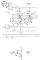
- FIG. 1 shows a writing device 1 which has a charge carrier source 2, which is connected via a circuit 3 to a voltage source 4, not shown, which has a first pole 5, a second pole 6 and a third pole 7.
- the first pole 5 forms an anode 8 and the second pole 6 forms a cathode 9.
- the arrangement is such that a plasma path 10 is ignited when an ignition voltage lying between anode 8 and cathode 9 is exceeded in charge carrier source 2, whereby free charge carriers, namely ions, are generated.
- a quiescent current forms in circuit 3, which maintains the plasma current flow.
- the current conditions can be controlled by a control device (which is not shown in FIG. 1) move, whereby ions in the direction of arrow 11 leave the circuit 3 and meet a substrate 12, whereby a targeted writing of the substrate with ions is possible.
- a plurality of charge carrier sources 2 are preferably provided, which are closely spaced from one another, that is to say highly integrated, opposite the substrate 12 and can each accumulate ions on the surface of the substrate 12 by means of control.
- the substrate 12 is constructed as a dielectric which is provided with a conductive layer which forms the pole 7. In this way, by appropriate control, a charge image can be generated on the surface of the substrate 12, which then — in a further process step, not shown in FIG. 1 — comes into contact with a colorant, as a result of which the colorant corresponds to the subject to be written bound and then fed to a printing material (for example paper).
- a printing material for example paper
- the anode 8 has a potential of> + 200 volts, in particular> + 300 volts.
- the cathode 9 has a potential which is in the O-volt potential range and above.
- the potential of the substrate 12, which is supplied to the voltage source 4 via the third pole 7, is preferably> 40 volts, in particular approximately 60 volts.
- FIG. 2 shows a current-voltage diagram of the plasma path 10 of the charge carrier source 2. It can be seen that when the voltage U rises, the plasma path ignites and then decreases considerably while the necessary rest voltage is reduced (in order to maintain the plasma current flow), even small changes in voltage leading to very large changes in current. For the operation of the writing device according to the invention it is therefore necessary to first ignite the individual plasma sections 10. Only then can you voltage jumps are generated in the circuit 3 by means of the associated control devices, which lead to ions being deposited on the substrate 12.
- FIG. 3 shows a block diagram of the writing device 1. It can be seen that a voltage pulse 13 is applied to the anode 8, which serves to ignite all the plasma lines 10. Once the ignition has taken place, the charge carrier sources 2 are in the stand-by mode already mentioned above. The voltage ratios are chosen so that no ions hit the substrate. Comparing the voltage pulse 13 with the illustration in FIG. 2, it becomes clear that it is necessary for the ignition of the plasma sections 10 to first apply the voltage U to the anode 8, which is greater than the voltage U peak according to FIG. 2. Once the ignition has taken place, the static operation is present, which requires a voltage U stat that is less than the voltage U peak . According to FIG.
- the voltage U stat is greater than the anode voltage U min running approximately parallel to the I axis (FIG. 2).
- these voltage ratios result in the advantage that only low voltage drops occur in the control path of the control device 17, which is important for a high integration density of the circuit.
- a switch S serves as an on-off switch, that is, it is closed for operation.
- Each charge carrier source 2 is advantageously assigned a series resistor Rv in the area of the anode 8, which serves to match the individual plasma paths 10 approximately identically to one another. The quiescent current is thus set constant everywhere.
- An electrical conductor 15 is connected to a connection 14 of the plasma path 10, which represents the cathode 9, which forms the opposite pole to the anode and which leads to an output stage 16 of the one already mentioned
- Control device 17 leads, which also has a logic 18 and a microprocessor 19.
- the control device 17 has a ground line 20, which forms the reference potential of the electronics, that is to say it is approximately at 0 volt potential with respect to the voltage source 4.
- An electronic control element (not shown), in particular a transistor or the like, is connected between the conductor 15 - and thus the cathode 9 - and the ground line 20, as a result of which the potential of the conductor 15 and thus the cathode 9 can be changed, in particular also down to the potential the ground line 20 is "pullable".
- This control element can also be a controllable resistor or the like.
- This variation possibility represents the control possibility of the control device 17. As already explained with reference to FIG. 1, it is possible to actively transfer ions in the direction of the arrow 11 to the substrate 12 by corresponding potential changes.
- control device and thus the associated advantages, in particular also the electronic components of the logic 18 and also of the microprocessor 19, are in a potential range which corresponds to the ground potential, so that the prevailing voltages are relatively low compared to the ground range. namely in the range of control voltages. In this way, flashovers and breakdowns can be avoided and an optimal high integration of the components can be realized. Smallest distances are possible, which means that extremely short switching times can be achieved.
- FIG. 4 shows a circuit section which has a switching transistor 21 which lies between the line 15 and the ground line 20 and can thus carry out the control function. Its base is connected to a Zener diode 22, which leads to the collector of the switching transistor 21. Is parallel to the Zener diode 22 a collector-emitter path of a further transistor 23, which serves as a driver. If - due to an impermissible operating state - the collector of the switching transistor 21 were supplied with too great a voltage, the driver transistor 23 breaks down and controls the switching transistor 21 in a corresponding manner, so that overall self-protection of the electronics is established.
Landscapes
- Printers Or Recording Devices Using Electromagnetic And Radiation Means (AREA)
- Non-Volatile Memory (AREA)
- Electrophotography Using Other Than Carlson'S Method (AREA)
Applications Claiming Priority (2)
| Application Number | Priority Date | Filing Date | Title |
|---|---|---|---|
| DE4413237 | 1994-04-15 | ||
| DE4413237A DE4413237A1 (de) | 1994-04-15 | 1994-04-15 | Schreibeinrichtung zum gesteuerten Aufbringen von Ladungsträgern auf ein Substrat |
Publications (2)
| Publication Number | Publication Date |
|---|---|
| EP0677391A2 true EP0677391A2 (fr) | 1995-10-18 |
| EP0677391A3 EP0677391A3 (fr) | 1998-01-07 |
Family
ID=6515627
Family Applications (1)
| Application Number | Title | Priority Date | Filing Date |
|---|---|---|---|
| EP95104246A Withdrawn EP0677391A3 (fr) | 1994-04-15 | 1995-03-23 | Dispositif d'inscription permettant de déposer des charges sur un substrat |
Country Status (4)
| Country | Link |
|---|---|
| US (1) | US5798782A (fr) |
| EP (1) | EP0677391A3 (fr) |
| JP (1) | JPH07290758A (fr) |
| DE (1) | DE4413237A1 (fr) |
Cited By (2)
| Publication number | Priority date | Publication date | Assignee | Title |
|---|---|---|---|---|
| US4566406A (en) * | 1983-07-13 | 1986-01-28 | Westinghouse Electric Corp. | Sludge removing apparatus for a steam generator |
| EP0876918A3 (fr) * | 1997-05-08 | 1999-08-04 | Heidelberger Druckmaschinen Aktiengesellschaft | Tête d'écriture électrostatique pour une machine d'impression électronique |
Family Cites Families (6)
| Publication number | Priority date | Publication date | Assignee | Title |
|---|---|---|---|---|
| US4524371A (en) * | 1983-04-01 | 1985-06-18 | Xerox Corporation | Modulation structure for fluid jet assisted ion projection printing apparatus |
| JPS61255870A (ja) * | 1985-05-10 | 1986-11-13 | Fuji Xerox Co Ltd | イオン流制御型記録ヘツド |
| JPS62144958A (ja) * | 1985-12-19 | 1987-06-29 | Fuji Xerox Co Ltd | イオン流静電記録装置 |
| US4763141A (en) * | 1987-08-03 | 1988-08-09 | Xerox Corporation | Printing apparatus with improved ion focus |
| JPH03230968A (ja) * | 1990-02-06 | 1991-10-14 | Fuji Xerox Co Ltd | 静電記録装置 |
| US5239317A (en) * | 1991-02-20 | 1993-08-24 | Kabushiki Kaisha Toshiba | Apparatus for generating ions in solid ion recording head with improved stability |
-
1994
- 1994-04-15 DE DE4413237A patent/DE4413237A1/de not_active Withdrawn
-
1995
- 1995-03-23 EP EP95104246A patent/EP0677391A3/fr not_active Withdrawn
- 1995-04-17 US US08/422,454 patent/US5798782A/en not_active Expired - Lifetime
- 1995-04-17 JP JP7090510A patent/JPH07290758A/ja active Pending
Cited By (2)
| Publication number | Priority date | Publication date | Assignee | Title |
|---|---|---|---|---|
| US4566406A (en) * | 1983-07-13 | 1986-01-28 | Westinghouse Electric Corp. | Sludge removing apparatus for a steam generator |
| EP0876918A3 (fr) * | 1997-05-08 | 1999-08-04 | Heidelberger Druckmaschinen Aktiengesellschaft | Tête d'écriture électrostatique pour une machine d'impression électronique |
Also Published As
| Publication number | Publication date |
|---|---|
| US5798782A (en) | 1998-08-25 |
| JPH07290758A (ja) | 1995-11-07 |
| EP0677391A3 (fr) | 1998-01-07 |
| DE4413237A1 (de) | 1995-10-19 |
Similar Documents
| Publication | Publication Date | Title |
|---|---|---|
| DE69105548T2 (de) | Vorrichtung zum Schutz gegen durch An- und Ausschaltung einer elektronischen Einheit an eine Gleichspannungsspeisung erzeugte Speisespannungsstörungen. | |
| DE69500086T2 (de) | Schaltungsanordnung zur Spannungsbegrenzung mit Hysteresiskomparator | |
| DE3125470C2 (fr) | ||
| DE4334513C1 (de) | CMOS-Schaltung mit erhöhter Spannungsfestigkeit | |
| DE3689986T2 (de) | Überwachungsschaltung für niedrige Spannungen. | |
| CH656818A5 (de) | Energiezuliefereinheit fuer eine funkenerosionsmaschine. | |
| DE102013105230A1 (de) | Treiberschaltkreis für einen Transistor | |
| DE3507130A1 (de) | Treiberstromkreis fuer eine magnetspule | |
| DE3615690C2 (de) | Integriertes Schutzelement, insbesondere für Eingänge in MOS-Technologie von integrierten Schaltungen | |
| DE2415098C3 (de) | Amplitudendetektorschaltung | |
| DE3842288A1 (de) | Schaltungsanordnung zur erzeugung einer konstanten bezugsspannung | |
| DE2336123A1 (de) | Bootstrap-schaltung | |
| EP0677391A2 (fr) | Dispositif d'inscription permettant de déposer des charges sur un substrat | |
| DE2137567B2 (de) | Elektronische Verstärkerschaltung zur Speisung einer Last mit einer Spannung, welche außergewöhnlich hohe Werte annehmen kann | |
| DE2056797B2 (de) | Schaltungsanordnung zur umschaltung einer kapazitiven last zwischen zwei potentialen | |
| DE10157524B4 (de) | Luftionisationsgerät | |
| DE19813964A1 (de) | Bussystem mit einer Zentraleinheit eine Mehrzahl von Steuermodulen, insbesondere für Insassenschutzsysteme in Kraftfahrzeugen | |
| DE3330383A1 (de) | Eingangsverstaerkerschaltung mit verbesserter rauschfreiheit | |
| DE2165160C2 (de) | CMOS-Schaltung als exklusives ODER-Glied | |
| WO2001011684A1 (fr) | Structure de protection contre les decharges electrostatiques (esd) | |
| EP3333656B1 (fr) | Circuiterie pour une entrée numérique d'un module périphérique et module périphérique | |
| DE69320631T2 (de) | Cmos stromsteuerschaltung | |
| DE102018207610B4 (de) | Schaltungsanordnung zum Begrenzen einer Spannung für eine an eine Kommunikationsleitung angeschlossene Kommunikationseinrichtung | |
| DE69611325T2 (de) | Schaltkreis zur selektiven Auswahl von Spannungen verschiedener Vorzeichen | |
| DE112020003959T5 (de) | Ausgabevorrichtung |
Legal Events
| Date | Code | Title | Description |
|---|---|---|---|
| PUAI | Public reference made under article 153(3) epc to a published international application that has entered the european phase |
Free format text: ORIGINAL CODE: 0009012 |
|
| 17P | Request for examination filed |
Effective date: 19950323 |
|
| AK | Designated contracting states |
Kind code of ref document: A2 Designated state(s): CH DE FR GB IT LI |
|
| GBC | Gb: translation of claims filed (gb section 78(7)/1977) | ||
| PUAL | Search report despatched |
Free format text: ORIGINAL CODE: 0009013 |
|
| AK | Designated contracting states |
Kind code of ref document: A3 Designated state(s): CH DE FR GB IT LI |
|
| 17Q | First examination report despatched |
Effective date: 19990115 |
|
| 18D | Application deemed to be withdrawn |
Effective date: 19990526 |