EP0678914A2 - Procédé de planarization d'un circuit intégré - Google Patents
Procédé de planarization d'un circuit intégré Download PDFInfo
- Publication number
- EP0678914A2 EP0678914A2 EP95301415A EP95301415A EP0678914A2 EP 0678914 A2 EP0678914 A2 EP 0678914A2 EP 95301415 A EP95301415 A EP 95301415A EP 95301415 A EP95301415 A EP 95301415A EP 0678914 A2 EP0678914 A2 EP 0678914A2
- Authority
- EP
- European Patent Office
- Prior art keywords
- gap distance
- oxide
- teos
- teos oxide
- thickness
- Prior art date
- Legal status (The legal status is an assumption and is not a legal conclusion. Google has not performed a legal analysis and makes no representation as to the accuracy of the status listed.)
- Withdrawn
Links
Images


Classifications
-
- H—ELECTRICITY
- H10—SEMICONDUCTOR DEVICES; ELECTRIC SOLID-STATE DEVICES NOT OTHERWISE PROVIDED FOR
- H10W—GENERIC PACKAGES, INTERCONNECTIONS, CONNECTORS OR OTHER CONSTRUCTIONAL DETAILS OF DEVICES COVERED BY CLASS H10
- H10W20/00—Interconnections in chips, wafers or substrates
- H10W20/01—Manufacture or treatment
- H10W20/071—Manufacture or treatment of dielectric parts thereof
- H10W20/092—Manufacture or treatment of dielectric parts thereof by smoothing the dielectric parts
-
- H—ELECTRICITY
- H10—SEMICONDUCTOR DEVICES; ELECTRIC SOLID-STATE DEVICES NOT OTHERWISE PROVIDED FOR
- H10P—GENERIC PROCESSES OR APPARATUS FOR THE MANUFACTURE OR TREATMENT OF DEVICES COVERED BY CLASS H10
- H10P95/00—Generic processes or apparatus for manufacture or treatments not covered by the other groups of this subclass
- H10P95/06—Planarisation of inorganic insulating materials
Definitions
- This invention relates to integrated circuit manufacture and more particularly to a method of forming a planarization structure of dielectric materials placed upon an integrated circuit topography which may, for example, form a highly planar interlevel dielectric structure having minimal stress properties.
- Manufacture of an integrated circuit involves numerous processing steps. Electronic devices must be patterned within a semiconductor substrate, and the patterned devices must be interconnected to one another to form a densely arranged integrated circuit. Due to rapid advances in layout density, interconnect between devices may involve numerous levels of interconnect stacked upon each other with a dielectric placed therebetween. Stacking of interconnect must be closely monitored to ensure that the interlevel dielectric is sufficient to electrically isolate the stacked conductors. Moreover, the interlevel dielectrics must be deposited in such a manner as to present a fairly even or smooth (i.e., planar) upper surface upon which a subsequent interconnect layer is placed. If the upper surface of the dielectric is not planar, then subsequent processing problems can occur such as step coverage and depth of focus problems.
- integrated circuit 10 includes a substrate 12 having an upper surface upon which a plurality of interconnect conductors 14 are arranged.
- Conductors 14 comprise one level of interconnect and, for illustrative purposes, comprise the first level of interconnect.
- a dielectric material 16 is placed above and between conductors 14.
- a second level of conductors can be placed upon the upper surface of dielectric 16 to form multilevel interconnects.
- another dielectric can be placed over the second level of conductors, and the process repeated depending upon the number of interconnect levels desired.
- the interlevel dielectric exhibit numerous mechanical as well as electrical properties. Electrically speaking, the dielectric must be substantially nonconductive and must provide a barrier against movement of mobile ions between conductive overlayers and conductive underlayers. Mechanically speaking, the dielectric must be easily etched, at a substantially uniform etch rate, and must exhibit conformal coverage and, if desired, highly planar coverage above and between uneven or non-planar underlayer. Providing a dielectric which is both conformal as well as having an upper surface which is substantially planar is difficult to achieve.
- Area 18 of densely patterned conductors 14 requires a substantially planar upper surface of dielectric 16.
- dielectric 16 must be conformal, but more importantly, dielectric 16 in area 18 must have an upper surface which is substantially planarized.
- Densely patterned conductors in area 18 form an uneven topography at the upper surface of dielectric 16 if dielectric 16 is not planarized. Resulting from an uneven dielectric upper surface is poor step coverage of subsequent conductors placed within area 18.
- Planarization in area 20 is not as crucial as in area 18. Namely, area 20 does not present severe unevenness at the upper surface of conductors 14 and, thereby, will not produce densely patterned disparities in the upper surface topography of dielectric 16.
- Fig. 2 not only illustrates the need for conformal dielectric 16 in area 20 and planarizable dielectric 16 in area 18, but also suggests problems associated with lack thereof.
- upper interconnect conductor 22a may experience step coverage problems.
- conductor 22b in area 20 may be larger (wider) than conductor 22a due to another problem often referred to as "depth of focus" problem. Depth of focus problem results from lithography process and, more specifically, from a disparity in resist removal caused by the relative depth of the resist being removed.
- the defocused area will cause a wider line width.
- An illustrated example is shown by the difference between the wider interconnect 22b than that of the narrower interconnect 22a.
- a shorter wavelength and a smaller numerical aperture of the optical projection source will lessen the depth of focus problem, but will not eliminate it. It is therefore essential that the upper surface of dielectric be maintained as a substantially uniform planar surface both to minimize step coverage problems and depth of focus problems.
- U.S. Patent No. 4,954,459 describes a dielectric which comprises either tetraethoxysilane (TEOS) or chemical vapor deposition (CVD) oxide. Select areas of the TEOS or CVD dielectric can be removed by subsequent etch-back and polishing steps in order to produce a highly planarized upper surface. While TEOS and CVD dielectrics are highly conformal, they are not highly planarizable unless subsequent etch-back and polishing steps are performed. Unfortunately, subsequent chemical or mechanical planarization steps (etch-back and polish) are time consuming and may leave additional contaminants upon the substrate topography.
- TEOS tetraethoxysilane
- CVD chemical vapor deposition
- SOG spin-on glasses
- SOGs often called organic silicates (which includes siloxanes), are applied in liquid form across the upper surface of the substrate in the same manner as, for example, photoresist. The liquid silicate is then heated to convert it to a silica film. The liquid silicate easily flows into any deformational valley at the upper surface of the interconnect topography in order to fill and thereby planarize the upper surface.
- SOG dielectrics are usually of a lower density than TEOS or CVD dielectrics.
- the SOG film undergoes a water sorption process that, when subjected to subsequent contact formation and aluminum deposition, causes water "outgassing" to occur. Water outgassing can lead to severe degradation and possible opencircuit failure in small contact windows etched through the SOG. See, e.g., Lifshitz, et al., "Water-Related Degradation of Contacts in the Multilevel MOS IC with Spin-On Glasses as Interlevel Dielectrics", IEEE Electron Device Letters, Vol. 10, No. 12, December 1989.
- TEOS and CVD dielectrics are highly conformal and perform well in sparsely patterned areas 20, they do not perform well in densely patterned areas 18.
- SOGs are well suited in densely patterned areas 18, but are usually avoided in sparsely patterned areas 20.
- TEOS and CVD oxides cannot be easily planarized to suit areas 18 and while SOGs exhibit water outgassing, neither dielectric, in and of itself, provides an adequate solution to the planarization problem. Accordingly, many researchers and manufacturers have focused upon an interlevel dielectric comprising both a deposited oxide (CVD or TEOS) and an SOG.
- the multi-layered dielectric structure achieves the advantage of presenting a highly conformal dielectric within area 20 and a planarized upper surface within area 18.
- the combinational dielectric structure often experiences severe cracking caused by intrinsic stresses within each layer as well as thermal expansivity problems between layers. It is possible that the primary source of the stress properties which cause cracking occur at the interface between the interconnect (or silicon substrate) and the dielectric.
- the dielectric comprises a sandwich structure of an SOG placed between CVD oxides. The CVD oxide which contacts the interconnect or substrate is subjected to significant thermal expansion stress at the juncture as well as inherent, intrinsic stress within the CVD (or TEOS) film.
- the interlevel dielectric structure comprises a plasma enhanced CVD (PECVD) oxide placed at the juncture between substrate (and/or interconnect) and overlying TEOS oxide.
- PECVD oxide is used to minimize the tensilly stressed TEOS overlayer.
- PECVD oxide is chosen as having a compressive stress factor which offsets the tensilly stressed TEOS oxide.
- PECVD oxide exhibits a lower expansion coefficient (relative to the underlayers of interconnect and substrate).
- a lower film expansivity difference between the PECVD and underlying substrate allows for a lower thermal mismatch at the juncture and therefore provides fewer stress points and possible cracks at the juncture as well as in the TEOS film.
- PECVD film is highly conformal to dense patterns of underlying interconnect (and substrate), and provides a good base topography adherence for overlying TEOS oxide. Furthermore, PECVD oxide helps reduce stress at the juncture between the interconnect and TEOS to allow a thicker TEOS oxide and the advantages thereof. In particular, a thicker TEOS oxide can be deposited having some advantages of planarization. A thicker TEOS oxide lacking substantial intrinsic tensile stress and thermal expansivity differential provides not only a high quality dielectric, but also can produce a base surface for receiving a planarization upper layer in densely patterned areas.
- thicker TEOS does provide some advantages of planarization
- thicker TEOS does not alone provide planarization absent an SOG overlayer.
- an SOG layer is deposited upon the thick TEOS oxide in order to fully planarize densely patterned areas and present an upper surface which is substantially uniform across the entire wafer topography.
- a capping layer of either PECVD oxide or TEOS oxide is formed above the SOG layer to (i) minimize sorption of water or hydrogen from the surrounding ambient into the SOG, and (ii) provide controlled thickness over areas in which a specific capacitance value is required.
- the entire SOG layer as well as the upper portions of TEOS oxide are removed prior to the placement or deposition of the capping layer.
- SOG and TEOS layers are etched at substantially the same rate so as to provide a resulting, substantially planar upper surface which is then capped using either PECVD or TEOS oxide.
- the TEOS oxide is formed within an atmospheric pressure CVD chamber using a TEOS and ozone ambient.
- the ozone, O3 is advantageously used to reduce the tensile stress within the TEOS oxide.
- the amount of O3 deposited within the TEOS can be adjusted. If O3 quantities are increased, then tensile stress is further reduced. A reduction in tensile stress reduces the amount of tensile stress, in relation to the compressive stress of the underlying PECVD oxide.
- a proper combination of the compressive stress of the underlayer PECVD oxide and the lower tensilly stressed TEOS oxide (as a result of O3) further minimizes the possibility of stress points or cracks within the combination dielectric.
- the present invention contemplates a method for forming a planarization structure of dielectric materials without removing the dielectric materials in non-contact areas prior to deposition of overlying conductors.
- the method comprises the steps of providing an integrated circuit topography comprising a plurality of conductors.
- the conductors are arranged at an elevation level disparity and at dissimilar pitch distances comprising a large gap distance and a small gap distance between the conductors.
- a plasma oxide is then deposited in a plasma enhanced CVD chamber upon the integrated circuit topography.
- a TEOS oxide is deposited upon the plasma oxide.
- the TEOS oxide is deposited in an atmospheric pressure CVD chamber and within a TEOS and ozone ambient.
- the TEOS oxide comprises a thickness which is larger in the small gap distance than in the large gap distance such that a TEOS oxide thickness disparity exists between TEOS oxide thickness in the large and small gap distances.
- a silicate (or siloxane) solution is spin deposited upon the TEOS oxide to form a silicate thickness which is larger in the large gap distance than in the small gap distance.
- Spin depositing the silicate solution is continued until a heating step causes the silicate solution to form a silica film having a substantially planarized upper surface.
- a silica thickness disparity exists between silica thickness in the large and small gap distances and the silica thickness disparity substantially equals the sum of the elevation level disparity and the TEOS oxide thickness disparity.
- a capping dielectric is placed upon the silica film to complete the planarization, dielectric structure.
- the present invention further contemplates an alternative exemplary methodology for forming a planarization structure which purposefully removes dielectric materials in non-contact areas prior to deposition of overlying conductors.
- the method utilizes the steps of providing an integrated circuit topography comprising a plurality of conductors having a large gap distance and a small gap distance between the conductors.
- a plasma oxide is then deposited upon the topography, and a TEOS oxide is deposited upon the plasma oxide.
- the TEOS oxide comprises a TEOS oxide upper surface in a small gap distance which is at a higher elevation level than the TEOS oxide upper surface in the large gap distance.
- a silicate solution is then deposited upon the TEOS oxide to form a silica film having a thickness which is larger in the large gap distance than in the small gap distance.
- the silica film comprises a silica upper surface which is substantially planar.
- the silica film and a portion of the TEOS oxide are removed at substantially the same removal rate to produce a final upper surface which is planarized at an elevation level substantially equal to the TEOS oxide upper surface in the large gap distance.
- a capping dielectric is then deposited upon the final upper surface.
- Integrated circuit 30 includes a silicon substrate 32 and area 34 of densely patterned conductors 38 as well as area 36 of sparsely patterned conductors 38.
- Conductors 38 can be somewhat thick (e.g., 3000 to 20,000 ⁇ ) and can be arranged in a dense fashion such as that normally found in a DRAM array.
- Conductors 38 are shown as the first layer or level of conductors. Subsequent layers are deposited and etched to form upper levels or layers of conductors, as described below. For simplicity, conductors 38 are illustrated substantially coplanar to each other.
- conductors 38 can be arranged in active and inactive (field oxide) regions at different elevation levels thereby comprising elevational disparity between conductors. Accordingly, the upper surfaces of conductors 38 are generally at different elevation levels above the silicon substrate and/or field oxides placed between substrate 32 and conductors 38. Moreover, it is understood that conductors 38 can be of any suitable conductive material including aluminum, aluminum silicide, polysilicon, etc.
- a plasma oxide 40 is deposited upon the upper surface of substrate 32 (and/or field oxides) as well as on the upper and side surfaces of conductors 38.
- Plasma oxide 40 is deposited at a thickness of approximately 2000 ⁇ , and is highly conformal about the upper topography.
- plasma oxide 40 conforms to the narrow spacing between conductors 38 and, depending upon said spacing, can form a thickness t1 greater than the thickness t2 in sparsely patterned area 36. Thickness t1, however, is not sufficiently thick so as to provide an upper planarized surface within area 34.
- the conformal nature of plasma oxide 40 thereby provides an initial disparity in the to-be-formed planarization structure. The initial disparity, however, is purposefully offset by subsequent dielectric layers.
- plasma oxide 40 is formed in the plasma enhanced CVD (PECVD) chamber.
- PECVD films utilize a reaction gas of, for example, silane (SiH4).
- silane reacts with, for example, oxygen or derivatives thereof, to form a reaction as follows: SiH4 + 2N2O ⁇ SiO2 + 2H2 + 2N2
- stoichiometry can deviate somewhat from SiO2 and a substantial amount of hydrogen may be incorporated in the resulting film.
- the benefit from PECVD is a lower temperature reaction.
- Silicon dioxide is formed at a temperature range from 200° C to 400° C, substantially less than the 600° C to 1200° C range for normal CVD reaction.
- Another important advantage of plasma oxide films generally relates to a lower internal or intrinsic stress property of the plasma film, as opposed to normal CVD films. Lower intrinsic stress plasma films are less likely to crack when they are deposited in thick layers.
- Intrinsic stress of plasma oxide 40 is measured in numerous ways. Generally speaking, stress is a function of expansion coefficient at the interface between layer 40 and underlayers as well as within in the internal properties of the film. Thus, total stress S is calculated as follows: Where ⁇ s is the expansion coefficient of the substrate and ⁇ f is the expansion coefficient of the oxide film. E f is Young's modulus of the film, ⁇ T is the deposition temperature minus room temperature, ⁇ f is Poisson's ratio of the oxide, and S i is the internal stress of the film. S i is process dependent and can be highly variable. Each of the above variables are well defined in semiconductor process technology and are well known to those skilled in the art. It is also well known that TEOS oxide is tensilly stressed.
- Tensile stress is measured as a positive stress from the above formula and is generally defined as a greater film expansivity than the underlying wafer (substrate) expansivity. Opposite to tensile stress is "compressive stress". Compressive stress involves a higher substrate expansivity than film expansivity. Being tensilly stressed, upper layers of TEOS oxide have a tendency to "pull apart" the internal structure of the TEOS as it is cooled. Resulting cracks in the TEOS oxide are common place unless compensated by an offsetting stress in an underlayer. Plasma oxides not only exhibit a lower intrinsic stress than do CVD oxides, but advantageously exhibit compressive stress.
- the compressive stress of oxide 40 functions to offset tensile stress of upper layer TEOS oxide to present a "stress balanced" dielectric structure. Accordingly, as circuit 30 cools after each and every thermal cycle, balanced stress between plasma oxide 40 and overlying TEOS oxide 42 (shown in Fig. 5) substantially prevents or minimizes cracks within the TEOS oxide. Any cracks which form within the dielectric can cause possible shorting paths between conductors 38 and overlying conductors 44 (shown in Figs. 8a and 8b).
- a stress balanced structure at the interface between TEOS oxide 42, plasma oxide 40 and substrate 32 is presented whereby the total stress does not exceed 1x10⁹ dynes/cm2 over the whole range of temperatures to which the films are subjected.
- stress balancing allows a thicker TEOS oxide 42 to be deposited than in conventional TEOS formations.
- TEOS oxide 42 is deposited at a thickness range of 6000 to 10000 ⁇ .
- the thicker oxide is substantially free of stress points and resulting cracks which would normally occur in a non-stress balanced structure.
- the thicker TEOS oxide provides a more planar upper surface 44 and a substantial disparity between the thickness t3 in region 34 and thickness t4 in region 36.
- Thickness disparity can range anywhere from 1:1.1 to over 1:1.3, whereas thickness t3 is advantageously greater than thickness t4. Thickness t3 is greater than thickness t4 so as to provide a somewhat planarized upper surface 44 in densely patterned, uneven substrate topography area 34. Additionally, upper surface 44 is relatively conformal in sparsely patterned region 36.
- the advantages of a thicker TEOS oxide 42 and thickness disparity (planarization) of the upper surface 44 will be made evident with reference to the remaining figures. It is important, however, that for reasons described below, the lowest elevational point for upper surface 44 is above any and all plasma oxide 40. A thicker TEOS oxide provides such elevational assurances.
- TEOS oxide 42 is formed upon plasma oxide 40 by placing substrate 32 (wafer) within an atmospheric pressure CVD (APCVD) reactor.
- a gas flow of TEOS in conjunction with ozone (O3) is placed in a flow pattern across the substrate upper surface.
- the TEOS and ozone mix and react in a gas phase upon the substrate upper surface leaving TEOS oxide 42 on oxide 40 while byproducts are evacuated from the reaction site. If the concentration of ozone is increased within the TEOS oxide, then tensile stress is correspondingly decreased. In order to ensure that sufficient amounts of ozone are placed within film 42, it is important that the ozone does not degrade prior to its deposition.
- a spin-on glass (SOG) film 46 such as an alkoxysilane, tetraethoxysilane methylsiloxane or acyloxysilane (each being placed in a solvent) is spin deposited on TEOS oxide 42.
- SOG spin-on glass
- a variety of well known spin-on polymers can also be used such as, for example, silsesquioxane.
- the liquid is then heated to convert it to a silica film.
- TEOS tetraethoxysilane
- a catalytic agent initiator
- heat is ordinarily used to covert the TEOS to silica.
- the doping agent itself for example, POCl3, may suffice as the initiator.
- a suitable siloxane-based SOG can be obtained from Allied-Signal, Milpitas, California, as tradename Accuglass® X-11 series product.
- SOG 46 can be deposited to thicknesses in the range of 1000 ⁇ to 9000 ⁇ and is heated in the range of 350° C to 450° C.
- the primary advantage of SOGs is the simplicity of applying a layer to a wafer, and have an additional advantage of topography planarization.
- upper surface 48 of SOG 46 is substantially planar, wherein the silica thickness t5 is greater than silica thickness t6 in regions 36 and 34, respectively.
- a thickness disparity between thicknesses t5 and t6 ranges anywhere from 1:1.1 to 1:2.0 in order to offset the thickness disparity in TEOS oxide 42 and thereby present a substantially planar upper surface 48.
- SOG film 46 presents many problems which can affect reliability of an integrated circuit.
- One problem stems from the lower density of SOG in relation to TEOS oxide or plasma oxide.
- the lower density SOG has a tendency to absorb water thereby causing "outgassing" of the water when contact windows are formed through the SOG. Outgassing of moisture in the contact windows adversely affects contact conductivity and should in most instances be avoided.
- One way to avoid the problems of SOG moisture absorption is to remove the entire SOG layer after its deposition -- i.e., remove a "sacrificial" SOG layer. Referring to Fig. 6b, SOG layer 46 is removed at substantially the same etch rate as the removal of underlying, upper portions of TEOS oxide 42.
- the substantially planar upper surface 48 can be maintained to an etch-back upper surface 50.
- a wet etchant such as HF
- Etch-back upper surface 50 is at approximately the same elevational level as the lowest elevation level of TEOS oxide 42 upper surface.
- a capping layer 52 can be deposited upon SOG layer 46 without previously removing the SOG layer. Capping layer 52 of Fig. 7a is therefore shown placed upon the upper surface 48 of SOG 46, illustrated in Fig. 6a.
- Capping layer 52 is preferably a CVD oxide and is formed as either a TEOS oxide or a plasma oxide. Preferably, however, capping layer 52 is a plasma oxide which is highly conformal to upper surface 48 of SOG 46. Capping layer 52 provides a barrier against water sorption into the underlying SOG from a moisture ambient.
- Capping layer 52 can be deposited at a controlled thickness upon SOG 46 to provide a close tolerance to capacitance value for the entire dielectric structure (plasma oxide 40, TEOS oxide 42 and SOG 46). Thus, capping layer 52 can have a variable thickness depending upon the desired capacitance outcome of the resulting dielectric. Any upper interconnect conductors placeable upon capping layer 52 incur a specific capacitance based upon the variability of the capping layer thickness relative to the remaining dielectric layers.
- capping layer 52 can be placed upon an etch-back upper surface 50 of Fig. 6b, as shown in Fig. 7b.
- Capping layer 52 in either embodiments of Fig. 7a or 7b, provide the advantages described above.
- Capping layer 52 upon etch-back upper surface 50, shown in Fig. 7b, ensures that the lower density TEOS oxide will not absorb moisture from an outside ambient.
- Capping layer 52 provides a barrier against absorption similar to the barrier formed above SOG layer 46, as shown in Fig. 7a.
- FIG. 8a upper interconnect conductors 44 are shown deposited upon the upper surface of capping layer 52.
- Conductors 44 form another level of conductors in a multi-level arrangement of interconnect. Multi-level conductors are commonly used in high density integrated circuit applications. It is understood that the procedures described in Figs. 3-7 can be repeated for numerous levels of interconnect (more than two) to achieve even higher interconnect densities.
- Conductors 44 of Fig. 8a are shown placed in the embodiments illustrated in the previous processing steps of Figs. 6a and 7a.
- Fig. 8b illustrates upper interconnect conductors 44 placed upon capping layer 52 subsequent to the processing steps of the embodiments illustrated in Figs. 6b and 7b.
- a desired outcome of the dielectric structure hereof is to not only achieve a upper planarized surface which produces minimal depth of focus problems, but also provides a dielectric with low stress properties and with a capping barrier against water or contamination absorption into the underlying dielectric.
- the resulting dielectric has low stress properties.
- stress is controlled by minimizing the intrinsic stress (tensile stress) within TEOS oxide 42.
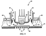
- Fig. 9 illustrates APCVD reactor 54 used for depositing TEOS oxide 42.
- Reactor 54 includes an injector 56 for injecting gaseous TEOS and ozone 58 into a mixing area directly above wafer 60.
- the unused material is purged through outlet exhaust 62 in the direction indicated by arrows 64.
- Nitrogen is often used as the purge carrier, and is generally inserted through purge curtains 66 and through perforations 68 arranged beneath conveyor belt 70 and wafer 60. Insertion of nitrogen carrier is shown along arrows 72.
- An APCVD system similar to that shown in Fig. 9, is available from, for example, Watkins-Johnson Company, Palo Alto, California. Functionality and structural description of a suitable Watkins-Johnson APCVD system is described in U.S. Patent No. 5,122,391 to Mayer (herein incorporated by reference).
- ozone provides an adjustable tensilly stressed TEOS oxide generally of less tensile stress than non-ozone TEOS oxide.
- the ozone TEOS provides a dielectric structure having a lesser tendency to crack and also provides an improved flow-like coverage in dense areas.
Landscapes
- Internal Circuitry In Semiconductor Integrated Circuit Devices (AREA)
- Formation Of Insulating Films (AREA)
- Local Oxidation Of Silicon (AREA)
Applications Claiming Priority (2)
| Application Number | Priority Date | Filing Date | Title |
|---|---|---|---|
| US229170 | 1994-04-18 | ||
| US08/229,170 US5503882A (en) | 1994-04-18 | 1994-04-18 | Method for planarizing an integrated circuit topography |
Publications (2)
| Publication Number | Publication Date |
|---|---|
| EP0678914A2 true EP0678914A2 (fr) | 1995-10-25 |
| EP0678914A3 EP0678914A3 (fr) | 1997-02-19 |
Family
ID=22860095
Family Applications (1)
| Application Number | Title | Priority Date | Filing Date |
|---|---|---|---|
| EP95301415A Withdrawn EP0678914A3 (fr) | 1994-04-18 | 1995-03-06 | Procédé de planarization d'un circuit intégré. |
Country Status (3)
| Country | Link |
|---|---|
| US (1) | US5503882A (fr) |
| EP (1) | EP0678914A3 (fr) |
| JP (1) | JPH07312368A (fr) |
Cited By (3)
| Publication number | Priority date | Publication date | Assignee | Title |
|---|---|---|---|---|
| EP0893825A1 (fr) * | 1997-07-23 | 1999-01-27 | STMicroelectronics S.r.l. | Méthode de planarisation d'un circuit électronique utilisant des multicouches |
| FR2776833A1 (fr) * | 1998-03-30 | 1999-10-01 | Samsung Electronics Co Ltd | Condensateur ferroelectrique et procede de fabrication d'un dispositif semi-conducteur le comprenant |
| FR2964245A1 (fr) * | 2010-08-30 | 2012-03-02 | Soitec Silicon On Insulator | Procede d'aplanissement |
Families Citing this family (44)
| Publication number | Priority date | Publication date | Assignee | Title |
|---|---|---|---|---|
| JPH0878406A (ja) * | 1994-09-08 | 1996-03-22 | Sony Corp | 酸化膜の成膜方法 |
| US5821163A (en) * | 1996-02-13 | 1998-10-13 | Vlsi Technology, Inc. | Method for achieving accurate SOG etchback selectivity |
| KR100230392B1 (ko) * | 1996-12-05 | 1999-11-15 | 윤종용 | 반도체 소자의 콘택 플러그 형성방법 |
| US5851867A (en) * | 1996-08-27 | 1998-12-22 | Mosel Vitellic Incorporated | Rugged stacked oxide layer structure and method of fabricating same |
| US6599847B1 (en) * | 1996-08-27 | 2003-07-29 | Taiwan Semiconductor Manufacturing Company | Sandwich composite dielectric layer yielding improved integrated circuit device reliability |
| US5786278A (en) * | 1996-08-27 | 1998-07-28 | Watkins-Johnson Company | Method of stress-relieving silicon oxide films |
| US6069069A (en) * | 1996-12-16 | 2000-05-30 | Chartered Semiconductor Manufacturing, Ltd. | Method for planarizing a low dielectric constant spin-on polymer using nitride etch stop |
| US5691247A (en) * | 1996-12-19 | 1997-11-25 | Tower Semiconductor Ltd. | Method for depositing a flow fill layer on an integrated circuit wafer |
| US6551665B1 (en) * | 1997-04-17 | 2003-04-22 | Micron Technology, Inc. | Method for improving thickness uniformity of deposited ozone-TEOS silicate glass layers |
| US5976979A (en) * | 1997-06-10 | 1999-11-02 | Industrial Technology Research Institute | Sequential oxygen plasma treatment and chemical mechanical polish (CMP) planarizing method for forming planarized low dielectric constant dielectric layer |
| TW396454B (en) * | 1997-06-24 | 2000-07-01 | Matsushita Electrics Corporati | Semiconductor device and method for fabricating the same |
| TW362269B (en) * | 1997-11-21 | 1999-06-21 | Promos Technologies Inc | Manufacturing method for improving the step coverage of titanium barrier capability |
| US6413583B1 (en) * | 1998-02-11 | 2002-07-02 | Applied Materials, Inc. | Formation of a liquid-like silica layer by reaction of an organosilicon compound and a hydroxyl forming compound |
| EP0948035A1 (fr) * | 1998-03-19 | 1999-10-06 | Applied Materials, Inc. | Méthode d'application d'un film diélectrique de recouvrement sur un empilement diélectrique |
| KR19990076407A (ko) * | 1998-03-31 | 1999-10-15 | 윤종용 | 반도체장치의 제조공정에 있어서의 박막 형성방법 |
| EP0954017A3 (fr) * | 1998-04-16 | 2000-08-09 | STMicroelectronics, Inc. | Structure semiconductrice avec une pile dielectrique 'pre-metal' améliorée |
| US6113465A (en) * | 1998-06-16 | 2000-09-05 | Speedfam-Ipec Corporation | Method and apparatus for improving die planarity and global uniformity of semiconductor wafers in a chemical mechanical polishing context |
| KR100518519B1 (ko) * | 1998-07-21 | 2005-11-25 | 삼성전자주식회사 | 반도체장치의 금속배선간 절연막 및 그 제조방법 |
| KR100480230B1 (ko) * | 1998-08-05 | 2005-07-05 | 주식회사 하이닉스반도체 | 반도체장치의금속배선형성방법 |
| US6800571B2 (en) * | 1998-09-29 | 2004-10-05 | Applied Materials Inc. | CVD plasma assisted low dielectric constant films |
| TW498433B (en) * | 1998-11-16 | 2002-08-11 | Taiwan Semiconductor Mfg | A surface planarization method |
| US6107186A (en) * | 1999-01-27 | 2000-08-22 | Advanced Micro Devices, Inc. | High planarity high-density in-laid metallization patterns by damascene-CMP processing |
| US6255232B1 (en) * | 1999-02-11 | 2001-07-03 | Taiwan Semiconductor Manufacturing Company | Method for forming low dielectric constant spin-on-polymer (SOP) dielectric layer |
| US6258643B1 (en) * | 1999-06-25 | 2001-07-10 | United Microelectronics Corp. | Method for forming twin gate CMOS |
| US6372664B1 (en) * | 1999-10-15 | 2002-04-16 | Taiwan Semiconductor Manufacturing Company | Crack resistant multi-layer dielectric layer and method for formation thereof |
| US6559020B1 (en) | 1999-10-20 | 2003-05-06 | Applied Micro Circuits Corporation | Bipolar device with silicon germanium (SiGe) base region |
| US6136688A (en) * | 1999-10-20 | 2000-10-24 | Vanguard International Semiconductor Corporation | High stress oxide to eliminate BPSG/SiN cracking |
| JP2004501503A (ja) * | 2000-03-07 | 2004-01-15 | マイクロン・テクノロジー・インコーポレーテッド | 集積回路におけるほとんど平坦な絶縁膜の形成方法 |
| US6635923B2 (en) * | 2001-05-24 | 2003-10-21 | International Business Machines Corporation | Damascene double-gate MOSFET with vertical channel regions |
| JP4318417B2 (ja) * | 2001-10-05 | 2009-08-26 | ソニー株式会社 | 高周波モジュール基板装置 |
| JP2004079988A (ja) * | 2002-06-19 | 2004-03-11 | Toshiba Corp | 半導体装置 |
| US6867129B2 (en) * | 2003-07-15 | 2005-03-15 | Taiwan Semiconductor Manufacturing Company | Method of improving the top plate electrode stress inducting voids for 1T-RAM process |
| KR100616187B1 (ko) * | 2004-10-07 | 2006-08-25 | 에스티마이크로일렉트로닉스 엔.브이. | 반도체 소자의 절연막 형성 방법 |
| KR100675895B1 (ko) * | 2005-06-29 | 2007-02-02 | 주식회사 하이닉스반도체 | 반도체소자의 금속배선구조 및 그 제조방법 |
| US20070048906A1 (en) * | 2005-08-23 | 2007-03-01 | Han Seung H | Method for fabricating semiconductor device |
| DE102006015096B4 (de) * | 2006-03-31 | 2011-08-18 | Globalfoundries Inc. | Verfahren zur Verringerung der durch Polieren hervorgerufenen Schäden in einer Kontaktstruktur durch Bilden einer Deckschicht |
| TWI396235B (zh) * | 2007-04-11 | 2013-05-11 | United Microelectronics Corp | 複合覆蓋層及其製作方法 |
| JP2009054683A (ja) * | 2007-08-24 | 2009-03-12 | Panasonic Corp | 半導体装置およびその製造方法 |
| CN101740467B (zh) * | 2008-11-24 | 2011-08-24 | 上海华虹Nec电子有限公司 | 半导体制造铝金属线制程 |
| US8883021B2 (en) | 2012-03-30 | 2014-11-11 | Taiwan Semiconductor Manufacturing Company, Ltd. | MEMS nanostructures and methods of forming the same |
| US8946095B2 (en) * | 2012-10-25 | 2015-02-03 | Taiwan Semiconductor Manufacturing Co., Ltd. | Method of forming interlayer dielectric film above metal gate of semiconductor device |
| CN104810277B (zh) * | 2014-01-26 | 2017-10-31 | 北大方正集团有限公司 | 一种晶圆表面平坦化工艺 |
| CN104795400B (zh) * | 2015-02-12 | 2018-10-30 | 合肥鑫晟光电科技有限公司 | 阵列基板制造方法、阵列基板和显示装置 |
| DE102020102533A1 (de) | 2020-01-31 | 2021-08-05 | Gesellschaft für angewandte Mikro- und Optoelektronik mit beschränkter Haftung - AMO GmbH | Verfahren zur Herstellung einer elektro-optischen Einrichtung, elektro-optische Einrichtung, Halbleitereinrichtung und Halbleitervorrichtung |
Family Cites Families (17)
| Publication number | Priority date | Publication date | Assignee | Title |
|---|---|---|---|---|
| US4407850A (en) * | 1982-01-11 | 1983-10-04 | The Perkin-Elmer Corporation | Profile control photoresist |
| JPH0642482B2 (ja) * | 1984-11-15 | 1994-06-01 | 株式会社東芝 | 半導体装置の製造方法 |
| US4872947A (en) * | 1986-12-19 | 1989-10-10 | Applied Materials, Inc. | CVD of silicon oxide using TEOS decomposition and in-situ planarization process |
| US4721548A (en) * | 1987-05-13 | 1988-01-26 | Intel Corporation | Semiconductor planarization process |
| CA2006174A1 (fr) * | 1989-12-20 | 1991-06-20 | Luc Ouellet | Methode de fabrication de films isolants sans craquelures au moyen de couches intermediaires de verre de spin |
| JP3128811B2 (ja) * | 1990-08-07 | 2001-01-29 | セイコーエプソン株式会社 | 半導体装置の製造方法 |
| US5089442A (en) * | 1990-09-20 | 1992-02-18 | At&T Bell Laboratories | Silicon dioxide deposition method using a magnetic field and both sputter deposition and plasma-enhanced cvd |
| DE4135810C2 (de) * | 1990-10-30 | 2000-04-13 | Mitsubishi Electric Corp | Halbleitereinrichtung mit einem Zwischenschichtisolierfilm und Verfahren zu deren Herstellung |
| JPH04223374A (ja) * | 1990-12-25 | 1992-08-13 | Mitsubishi Electric Corp | 固体撮像装置の製造方法 |
| DE69130947T2 (de) * | 1991-01-08 | 1999-07-08 | Fujitsu Ltd., Kawasaki, Kanagawa | Verfahren zur bildung eines siliciumoxid-filmes |
| US5279865A (en) * | 1991-06-28 | 1994-01-18 | Digital Equipment Corporation | High throughput interlevel dielectric gap filling process |
| US5252515A (en) * | 1991-08-12 | 1993-10-12 | Taiwan Semiconductor Manufacturing Company | Method for field inversion free multiple layer metallurgy VLSI processing |
| JPH05235184A (ja) * | 1992-02-26 | 1993-09-10 | Nec Corp | 半導体装置の多層配線構造体の製造方法 |
| US5286518A (en) * | 1992-04-30 | 1994-02-15 | Vlsi Technology, Inc. | Integrated-circuit processing with progressive intermetal-dielectric deposition |
| US5356722A (en) * | 1992-06-10 | 1994-10-18 | Applied Materials, Inc. | Method for depositing ozone/TEOS silicon oxide films of reduced surface sensitivity |
| EP0582724A1 (fr) * | 1992-08-04 | 1994-02-16 | Siemens Aktiengesellschaft | Procédé de dépôt chimique en phase vapeur de couches de SiO2 planarisées localement et globalement sur des substrats en silicium structurés |
| US5403780A (en) * | 1993-06-04 | 1995-04-04 | Jain; Vivek | Method enhancing planarization etchback margin, reliability, and stability of a semiconductor device |
-
1994
- 1994-04-18 US US08/229,170 patent/US5503882A/en not_active Expired - Lifetime
-
1995
- 1995-03-06 EP EP95301415A patent/EP0678914A3/fr not_active Withdrawn
- 1995-04-18 JP JP7092365A patent/JPH07312368A/ja not_active Withdrawn
Cited By (3)
| Publication number | Priority date | Publication date | Assignee | Title |
|---|---|---|---|---|
| EP0893825A1 (fr) * | 1997-07-23 | 1999-01-27 | STMicroelectronics S.r.l. | Méthode de planarisation d'un circuit électronique utilisant des multicouches |
| FR2776833A1 (fr) * | 1998-03-30 | 1999-10-01 | Samsung Electronics Co Ltd | Condensateur ferroelectrique et procede de fabrication d'un dispositif semi-conducteur le comprenant |
| FR2964245A1 (fr) * | 2010-08-30 | 2012-03-02 | Soitec Silicon On Insulator | Procede d'aplanissement |
Also Published As
| Publication number | Publication date |
|---|---|
| US5503882A (en) | 1996-04-02 |
| EP0678914A3 (fr) | 1997-02-19 |
| JPH07312368A (ja) | 1995-11-28 |
Similar Documents
| Publication | Publication Date | Title |
|---|---|---|
| US5503882A (en) | Method for planarizing an integrated circuit topography | |
| US5607773A (en) | Method of forming a multilevel dielectric | |
| KR100288827B1 (ko) | 반도체장치 및 그 제조방법 | |
| US5578524A (en) | Fabrication process of a semiconductor device with a wiring structure | |
| EP0496614A1 (fr) | Procéde pour la formation d'ouvertures de contact lors de la fabrication de dispositif à semiconducteur | |
| US6187662B1 (en) | Semiconductor device with low permittivity interlayer insulating film and method of manufacturing the same | |
| US7196422B2 (en) | Low-dielectric constant structure with a multilayer stack of thin films with pores | |
| KR100382376B1 (ko) | 반도체 장치 및 그의 제조방법 | |
| US12087692B2 (en) | Hardened interlayer dielectric layer | |
| JP4168397B2 (ja) | 高アスペクト比の半導体デバイス用のボロンドープ窒化チタン層 | |
| US5366850A (en) | Submicron planarization process with passivation on metal line | |
| US5502006A (en) | Method for forming electrical contacts in a semiconductor device | |
| KR100562541B1 (ko) | Cvd 실리콘 옥시나이트라이드층에 의해 후처리되는sion/teos 층간 유전체 형성 방법 | |
| US6846737B1 (en) | Plasma induced depletion of fluorine from surfaces of fluorinated low-k dielectric materials | |
| KR100248572B1 (ko) | 반도체장치 및 그제조방법 | |
| US6472751B1 (en) | H2 diffusion barrier formation by nitrogen incorporation in oxide layer | |
| US6727160B1 (en) | Method of forming a shallow trench isolation structure | |
| JP2001118928A (ja) | 集積回路の製造方法 | |
| JP2953447B2 (ja) | 溝分離型半導体装置の製造方法 | |
| US6580155B1 (en) | Semiconductor device | |
| US10957531B2 (en) | Method of manufacturing semiconductor device | |
| JP4028032B2 (ja) | 半導体装置及びその製造方法 | |
| KR100248159B1 (ko) | 반도체장치에 있어서 이온주입을 통한 에스오지층형성방법 | |
| US20050112877A1 (en) | Method of manufacturing a semiconductor device | |
| KR100265357B1 (ko) | 반도체장치의콘택홀형성방법 |
Legal Events
| Date | Code | Title | Description |
|---|---|---|---|
| PUAI | Public reference made under article 153(3) epc to a published international application that has entered the european phase |
Free format text: ORIGINAL CODE: 0009012 |
|
| AK | Designated contracting states |
Kind code of ref document: A2 Designated state(s): AT BE DE DK ES FR GB GR IE IT LU NL PT SE |
|
| PUAL | Search report despatched |
Free format text: ORIGINAL CODE: 0009013 |
|
| AK | Designated contracting states |
Kind code of ref document: A3 Designated state(s): AT BE DE DK ES FR GB GR IE IT LU NL PT SE |
|
| 17P | Request for examination filed |
Effective date: 19970723 |
|
| 17Q | First examination report despatched |
Effective date: 19971003 |
|
| 18D | Application deemed to be withdrawn |
Effective date: 19990323 |