EP0678918A2 - Circuit imprimé multi-couche - Google Patents
Circuit imprimé multi-couche Download PDFInfo
- Publication number
- EP0678918A2 EP0678918A2 EP95302211A EP95302211A EP0678918A2 EP 0678918 A2 EP0678918 A2 EP 0678918A2 EP 95302211 A EP95302211 A EP 95302211A EP 95302211 A EP95302211 A EP 95302211A EP 0678918 A2 EP0678918 A2 EP 0678918A2
- Authority
- EP
- European Patent Office
- Prior art keywords
- insulating
- interlaminar
- layers
- insulating layers
- glass transition
- Prior art date
- Legal status (The legal status is an assumption and is not a legal conclusion. Google has not performed a legal analysis and makes no representation as to the accuracy of the status listed.)
- Withdrawn
Links
Images


Classifications
-
- H—ELECTRICITY
- H05—ELECTRIC TECHNIQUES NOT OTHERWISE PROVIDED FOR
- H05K—PRINTED CIRCUITS; CASINGS OR CONSTRUCTIONAL DETAILS OF ELECTRIC APPARATUS; MANUFACTURE OF ASSEMBLAGES OF ELECTRICAL COMPONENTS
- H05K3/00—Apparatus or processes for manufacturing printed circuits
- H05K3/46—Manufacturing multilayer circuits
- H05K3/4688—Composite multilayer circuits, i.e. comprising insulating layers having different properties
-
- H—ELECTRICITY
- H05—ELECTRIC TECHNIQUES NOT OTHERWISE PROVIDED FOR
- H05K—PRINTED CIRCUITS; CASINGS OR CONSTRUCTIONAL DETAILS OF ELECTRIC APPARATUS; MANUFACTURE OF ASSEMBLAGES OF ELECTRICAL COMPONENTS
- H05K1/00—Printed circuits
- H05K1/02—Details
-
- H—ELECTRICITY
- H05—ELECTRIC TECHNIQUES NOT OTHERWISE PROVIDED FOR
- H05K—PRINTED CIRCUITS; CASINGS OR CONSTRUCTIONAL DETAILS OF ELECTRIC APPARATUS; MANUFACTURE OF ASSEMBLAGES OF ELECTRICAL COMPONENTS
- H05K3/00—Apparatus or processes for manufacturing printed circuits
- H05K3/46—Manufacturing multilayer circuits
- H05K3/4611—Manufacturing multilayer circuits by laminating two or more circuit boards
- H05K3/4623—Manufacturing multilayer circuits by laminating two or more circuit boards the circuit boards having internal via connections between two or more circuit layers before lamination, e.g. double-sided circuit boards
-
- H—ELECTRICITY
- H05—ELECTRIC TECHNIQUES NOT OTHERWISE PROVIDED FOR
- H05K—PRINTED CIRCUITS; CASINGS OR CONSTRUCTIONAL DETAILS OF ELECTRIC APPARATUS; MANUFACTURE OF ASSEMBLAGES OF ELECTRICAL COMPONENTS
- H05K3/00—Apparatus or processes for manufacturing printed circuits
- H05K3/46—Manufacturing multilayer circuits
- H05K3/4611—Manufacturing multilayer circuits by laminating two or more circuit boards
- H05K3/4626—Manufacturing multilayer circuits by laminating two or more circuit boards characterised by the insulating layers or materials
-
- H—ELECTRICITY
- H05—ELECTRIC TECHNIQUES NOT OTHERWISE PROVIDED FOR
- H05K—PRINTED CIRCUITS; CASINGS OR CONSTRUCTIONAL DETAILS OF ELECTRIC APPARATUS; MANUFACTURE OF ASSEMBLAGES OF ELECTRICAL COMPONENTS
- H05K3/00—Apparatus or processes for manufacturing printed circuits
- H05K3/46—Manufacturing multilayer circuits
- H05K3/4697—Manufacturing multilayer circuits having cavities, e.g. for mounting components
-
- H—ELECTRICITY
- H10—SEMICONDUCTOR DEVICES; ELECTRIC SOLID-STATE DEVICES NOT OTHERWISE PROVIDED FOR
- H10W—GENERIC PACKAGES, INTERCONNECTIONS, CONNECTORS OR OTHER CONSTRUCTIONAL DETAILS OF DEVICES COVERED BY CLASS H10
- H10W70/00—Package substrates; Interposers; Redistribution layers [RDL]
- H10W70/01—Manufacture or treatment
- H10W70/05—Manufacture or treatment of insulating or insulated package substrates, or of interposers, or of redistribution layers
-
- H—ELECTRICITY
- H10—SEMICONDUCTOR DEVICES; ELECTRIC SOLID-STATE DEVICES NOT OTHERWISE PROVIDED FOR
- H10W—GENERIC PACKAGES, INTERCONNECTIONS, CONNECTORS OR OTHER CONSTRUCTIONAL DETAILS OF DEVICES COVERED BY CLASS H10
- H10W70/00—Package substrates; Interposers; Redistribution layers [RDL]
- H10W70/60—Insulating or insulated package substrates; Interposers; Redistribution layers
- H10W70/611—Insulating or insulated package substrates; Interposers; Redistribution layers for connecting multiple chips together
-
- H—ELECTRICITY
- H10—SEMICONDUCTOR DEVICES; ELECTRIC SOLID-STATE DEVICES NOT OTHERWISE PROVIDED FOR
- H10W—GENERIC PACKAGES, INTERCONNECTIONS, CONNECTORS OR OTHER CONSTRUCTIONAL DETAILS OF DEVICES COVERED BY CLASS H10
- H10W70/00—Package substrates; Interposers; Redistribution layers [RDL]
- H10W70/60—Insulating or insulated package substrates; Interposers; Redistribution layers
- H10W70/67—Insulating or insulated package substrates; Interposers; Redistribution layers characterised by their insulating layers or insulating parts
- H10W70/68—Shapes or dispositions thereof
- H10W70/685—Shapes or dispositions thereof comprising multiple insulating layers
-
- H—ELECTRICITY
- H10—SEMICONDUCTOR DEVICES; ELECTRIC SOLID-STATE DEVICES NOT OTHERWISE PROVIDED FOR
- H10W—GENERIC PACKAGES, INTERCONNECTIONS, CONNECTORS OR OTHER CONSTRUCTIONAL DETAILS OF DEVICES COVERED BY CLASS H10
- H10W70/00—Package substrates; Interposers; Redistribution layers [RDL]
- H10W70/60—Insulating or insulated package substrates; Interposers; Redistribution layers
- H10W70/67—Insulating or insulated package substrates; Interposers; Redistribution layers characterised by their insulating layers or insulating parts
- H10W70/69—Insulating materials thereof
- H10W70/695—Organic materials
-
- H—ELECTRICITY
- H05—ELECTRIC TECHNIQUES NOT OTHERWISE PROVIDED FOR
- H05K—PRINTED CIRCUITS; CASINGS OR CONSTRUCTIONAL DETAILS OF ELECTRIC APPARATUS; MANUFACTURE OF ASSEMBLAGES OF ELECTRICAL COMPONENTS
- H05K2201/00—Indexing scheme relating to printed circuits covered by H05K1/00
- H05K2201/01—Dielectrics
- H05K2201/0137—Materials
- H05K2201/0154—Polyimide
-
- H—ELECTRICITY
- H05—ELECTRIC TECHNIQUES NOT OTHERWISE PROVIDED FOR
- H05K—PRINTED CIRCUITS; CASINGS OR CONSTRUCTIONAL DETAILS OF ELECTRIC APPARATUS; MANUFACTURE OF ASSEMBLAGES OF ELECTRICAL COMPONENTS
- H05K3/00—Apparatus or processes for manufacturing printed circuits
- H05K3/46—Manufacturing multilayer circuits
- H05K3/4644—Manufacturing multilayer circuits by building the multilayer layer by layer, i.e. build-up multilayer circuits
- H05K3/4673—Application methods or materials of intermediate insulating layers not specially adapted to any one of the previous methods of adding a circuit layer
- H05K3/4676—Single layer compositions
-
- H—ELECTRICITY
- H10—SEMICONDUCTOR DEVICES; ELECTRIC SOLID-STATE DEVICES NOT OTHERWISE PROVIDED FOR
- H10W—GENERIC PACKAGES, INTERCONNECTIONS, CONNECTORS OR OTHER CONSTRUCTIONAL DETAILS OF DEVICES COVERED BY CLASS H10
- H10W70/00—Package substrates; Interposers; Redistribution layers [RDL]
- H10W70/60—Insulating or insulated package substrates; Interposers; Redistribution layers
- H10W70/67—Insulating or insulated package substrates; Interposers; Redistribution layers characterised by their insulating layers or insulating parts
- H10W70/68—Shapes or dispositions thereof
- H10W70/682—Shapes or dispositions thereof comprising holes having chips therein
-
- H—ELECTRICITY
- H10—SEMICONDUCTOR DEVICES; ELECTRIC SOLID-STATE DEVICES NOT OTHERWISE PROVIDED FOR
- H10W—GENERIC PACKAGES, INTERCONNECTIONS, CONNECTORS OR OTHER CONSTRUCTIONAL DETAILS OF DEVICES COVERED BY CLASS H10
- H10W72/00—Interconnections or connectors in packages
- H10W72/071—Connecting or disconnecting
- H10W72/075—Connecting or disconnecting of bond wires
- H10W72/07551—Connecting or disconnecting of bond wires characterised by changes in properties of the bond wires during the connecting
- H10W72/07554—Connecting or disconnecting of bond wires characterised by changes in properties of the bond wires during the connecting changes in dispositions
-
- H—ELECTRICITY
- H10—SEMICONDUCTOR DEVICES; ELECTRIC SOLID-STATE DEVICES NOT OTHERWISE PROVIDED FOR
- H10W—GENERIC PACKAGES, INTERCONNECTIONS, CONNECTORS OR OTHER CONSTRUCTIONAL DETAILS OF DEVICES COVERED BY CLASS H10
- H10W72/00—Interconnections or connectors in packages
- H10W72/50—Bond wires
- H10W72/531—Shapes of wire connectors
- H10W72/5363—Shapes of wire connectors the connected ends being wedge-shaped
-
- H—ELECTRICITY
- H10—SEMICONDUCTOR DEVICES; ELECTRIC SOLID-STATE DEVICES NOT OTHERWISE PROVIDED FOR
- H10W—GENERIC PACKAGES, INTERCONNECTIONS, CONNECTORS OR OTHER CONSTRUCTIONAL DETAILS OF DEVICES COVERED BY CLASS H10
- H10W72/00—Interconnections or connectors in packages
- H10W72/50—Bond wires
- H10W72/541—Dispositions of bond wires
- H10W72/547—Dispositions of multiple bond wires
-
- H—ELECTRICITY
- H10—SEMICONDUCTOR DEVICES; ELECTRIC SOLID-STATE DEVICES NOT OTHERWISE PROVIDED FOR
- H10W—GENERIC PACKAGES, INTERCONNECTIONS, CONNECTORS OR OTHER CONSTRUCTIONAL DETAILS OF DEVICES COVERED BY CLASS H10
- H10W90/00—Package configurations
- H10W90/701—Package configurations characterised by the relative positions of pads or connectors relative to package parts
- H10W90/751—Package configurations characterised by the relative positions of pads or connectors relative to package parts of bond wires
- H10W90/754—Package configurations characterised by the relative positions of pads or connectors relative to package parts of bond wires between a chip and a stacked insulating package substrate, interposer or RDL
-
- Y—GENERAL TAGGING OF NEW TECHNOLOGICAL DEVELOPMENTS; GENERAL TAGGING OF CROSS-SECTIONAL TECHNOLOGIES SPANNING OVER SEVERAL SECTIONS OF THE IPC; TECHNICAL SUBJECTS COVERED BY FORMER USPC CROSS-REFERENCE ART COLLECTIONS [XRACs] AND DIGESTS
- Y10—TECHNICAL SUBJECTS COVERED BY FORMER USPC
- Y10T—TECHNICAL SUBJECTS COVERED BY FORMER US CLASSIFICATION
- Y10T428/00—Stock material or miscellaneous articles
- Y10T428/24—Structurally defined web or sheet [e.g., overall dimension, etc.]
- Y10T428/24802—Discontinuous or differential coating, impregnation or bond [e.g., artwork, printing, retouched photograph, etc.]
- Y10T428/24917—Discontinuous or differential coating, impregnation or bond [e.g., artwork, printing, retouched photograph, etc.] including metal layer
Definitions
- the present invention relates to a multilayer printed wiring board, particularly one used for semiconductor chip package, and a process for producing such a wiring board.
- Multilayer printed wiring board usually comprises an insulating substrate, a power layer, a ground layer, circuit conductors formed on the surface thereof, inner layer circuits, via holes or through-holes for making electrical connection of the circuits in the respective layers, and solder resists for insulating the surface circuits.
- a method which comprises forming the inner circuits and interlayer circuit boards including a power layer and a ground layer by etching away unnecessary parts of the copper foil of a copper-clad laminate, placing thereon a prepreg and a copper foil in layers, integrally laminating them by heating under pressure, forming openings at the parts where electrical connection is to be made, metallizing the inner walls of said openings by electroless plating or other means, etching away the unnecessary parts of the copper foil on the surface, then coating a solder resist thereon and drying the same.
- the inner layer circuits of the respective layers are formed separately and positioned by using guide pins, and after integral lamination, the through-holes, outer layer circuits and solder resist are formed.
- JP-A- Japanese Patent Application Kokai (Laid-Open) [JP-A-] No. 59-158579 discloses a leadless chip carrier in which the terminals connected to semiconductor chips are extended out from the inside to a part on the outside of the package.
- JP-B-]No. 58-11100 discloses a pin grid array having a plurality of terminal pins for connection to the through-holes in other package-carrying wiring boards, and a process for producing such an array.
- This patent also presents a ball grid array in which solder balls are fused to the lands instead of pins in the pin grid array to make electrical connection by soldering.
- JP-B-58-26828 discloses a tape automatic carrier constituted by first forming the terminal strips and then insulating them with a tape-like insulating film.
- chip carriers In most of these semiconductor chip packages (hereinafter referred to as "chip carriers"), a ceramic material has been used for insulators and electrical connection of these chip carriers to semiconductor chip terminals has been made by wire bonding. Organic insulating material has been used as sealant for protecting the semiconductor chips and electrical connections from the environment after the semiconductor chips have been mounted on said chip carriers.
- chip carrier producing methods incorporating the ordinary multilayer wiring board manufacturing techniques using an organic insulating material.
- a method for producing pin grid array packages is disclosed in JP-B-3-25023.
- the conventional prepregs using woven or non-woven glass fabrics are capable of answering to such request for size reduction, and it is therefore attempted to apply an insulating resin or to use a film of insulating resin.
- This phenomenon tends to occur particularly when the through-holes are formed in the multilayer wiring board or when many via holes are formed in the layers containing no reinforcement such as woven or non-woven glass fabrics.
- the present invention has for its object to provide a multilayer printed wiring board which is proof against exfoliation of laminations due to heat history of the board and has high reliability of insulation and electrical connection by through-holes, and a process for producing such a multilayer printed wiring board.
- the present invention provides a multilayer printed wiring board comprising a plurality of interlaminar insulating layers, a plurality of insulating substrates containing a reinforcement, circuits formed on the surfaces of said insulating substrates, and via holes for making electrical connection between at least two layers of circuits, wherein said via holes run through the two layers of insulating substrates and the interlaminar insulating layer disposed therebetween, said interlaminar insulating layers being the layers not containing a reinforcement, and further characterized in that the B-stage resin flow of said insulating layers is less than 1%, and that the difference between the glass transition point of said interlaminar insulating layer and that of the insulating substrate adjacent thereto is not greater than 60°C.
- the present invention also provides a process for producing a multilayer printed wiring board, which comprises integrally laminating, by heating under pressure, B-staged interlaminar insulating layers and insulating circuit boards having circuits formed on the reinforcement-containing insulating substrates, and forming via holes for electrical connection between two or more layers of circuits, wherein said via holes run through two layers of insulating substrates and the interlaminar insulating layer disposed therebetween, said interlaminar insulating layers being the insulating layers not containing a reinforcement, and further characterized in that the B-stage resin flow of said insulating layers is less than 1%, and that the difference between the glass transition point of said interlaminar insulating layer and that of the insulating substrate adjacent thereto is not greater than 60°C.
- FIG. 1 is a diagrammatic sectional view for illustrating the structural features of the present invention.
- FIGS. 2A to 2C are diagrammatic sectional views for illustrating an example of use of the present invention.
- FIG. 3 is a diagrammatic sectional view showing a mode of practice of the present invention.
- FIGS. 4A and 4B are diagrammatic sectional views for illustrating the process of the present invention.
- FIGS. 5A to 5C are diagrammatic sectional views showing another mode of practice of the present invention.
- FIGS. 6A to 6G are diagrammatic fragmentary sectional views for illustrating the structure of the present invention.
- FIG. 7 is a diagrammatic sectional view for illustrating the process in an embodiment of the present invention.
- FIGS. 8A to 8E are diagrammatic sectional views for illustrating the respective steps in the process according to an embodiment of the present invention.
- FIGS. 9A to 9D are diagrammatic sectional views for illustrating the respective steps in the process according to another embodiment of the present invention.
- FIG. 10 is a diagrammatic sectional view showing still another embodiment of the present invention.
- FIGS. 11A to 11D are diagrammatic sectional views for illustrating the prior art problems.
- FIGS. 12A to 12G are diagrammatic sectional views for illustrating an example of production process according to the present invention.
- FIGS. 13A to 13G are diagrammatic sectional views for illustrating another example of production process according to the present invention.
- FIGS. 14A to 14D are diagrammatic sectional views for illustrating still another example of production process according to the present invention.
- the multilayer printed wiring board according to the present invention comprises a plurality of interlaminar insulating layers, a plurality of insulating substrates containing a reinforcing material and laminated alternately, circuits formed on the surfaces of said insulating substrates, and via holes for making electrical connection between two or more layers of circuits, wherein said via holes run through two layers of insulating substrates and the interlaminar insulating layer formed therebetween, said interlaminar insulating layers being the insulating layers not containing a reinforcement, and further characterized in that the B-stage resin flow of said insulating layers is less than 1%, and that the difference between the glass transition point of the interlaminar insulating layer and that of the insulating substrate adjacent thereto is not greater than 60°C.
- the glass transition point of these materials is investigated and those having the above-defined difference (not greater than 60°C) in glass transition point are selected and used for the adjoining laminations.
- the difference in glass transition point is preferably not greater than 40°C.
- the difference in glass transition point between the one with the highest glass transition point and the one with the lowest glass transition point is not greater than 30°C.
- the insulating substrates used in the present invention comprise reinforcing fiber such as glass cloth, glass paper, glass short fiber or the like impregnated with an appropriate resin such as epoxy resin, polyimide resin or the like for inhibiting change of size due to heat history in the course of working.
- the material usable for the insulating substrates disposed adjacent to said respective insulating layers is one having a glass transition point of 70-165°C.
- examples of such material are a polymeric polyimide-type adhesive film AS-3000 (mentioned above), an epoxy resin-impregnated prepreg GEA-67 (trade name, available from Hitachi Chemical Co., Ltd.) and an epoxy solder resist CCR-506(trade name, available from Asahi Chemical Laboratory, Ltd.).
- the material usable for the adjoining insulating substrates is one having a glass transition point of 110-225°C.
- Examples of such material are a polyimide-type adhesive film AS-2250 or 2210 (mentioned above), an epoxy resin-impregnated prepreg GEA-679 (trade name, available from Hitachi Chemical Co., Ltd.) and a heat resistant thermosetting BT resin (containing triazine component and bismaleimide component as fundamental components)-type prepreg GHPL-830 (trade name, available from Mitsubishi Gas Chemical Co., Ltd.).
- the material usable for the adjoining insulating layers is one having a glass transition point of 55-160°C, such as an epoxy solder resist CCR-506 (mentioned above), a polymeric polyimide-type adhesive film AS-3000 (mentioned above), an epoxy resin-impregnated prepreg GEA-67 (mentioned above) and the like.
- solder resist ink generally employed in the manufacture of wiring boards, and the type of ink to be used can be properly selected in consideration to the above-defined range of glass transition point.
- a varnish is applied on the support film and dried into an adhesive film so that said layers can be used in the B-stage state.
- the B-stage resin flow of said layers is less than 1%, and the B-stage viscoelasticity of said layers is in the range of 2,000-5,000 MPa at 30°C and in the range below 10 MPa at the molding temperature.
- the layer materials satisfying these requirements include polymeric epoxy film, polyimide film and epoxy solder resist ink.
- the film in the state of B stage there can be used, for example, such commercial products as AS-3000 (polymeric epoxy adhesive film) and AS-2250 and 2210 (polyimide adhesive film, both mentioned above).
- a plurality of B-staged interlaminar insulating layers 1 and insulating substrates 21 are selected so that the difference in glass transition point between the adjoining insulating layers will fall in the range not exceeding 60°C, and said interlaminar insulating layers and insulating circuit boards 2 having circuits 22 formed on the insulating substrates are integrally laminated by heating under pressure, and then via holes for making electrical connection between two or more layers of circuits are formed. Said via holes run through two layers of said insulating substrates and the interlaminar insulating layer disposed therebetween.
- Said interlaminar insulating layers are the insulating layers containing no reinforcement such as woven or nonwoven glass fabrics.
- the B-stage resin flow of said insulating layers is less than 1%, and the difference in glass transition point between an insulating layer and the insulating substrate adjacent thereto is not greater than 60°C.
- Such a multilayer printed wiring board can also be produced according to the following processes (a)-(d).
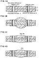
- etching resists are provided at the parts where circuits are to be formed on a laminate comprising copper-clad insulating substrates containing reinforcing fiber, such as shown in FIG. 12A, to constitute an insulating circuit board as shown in FIG. 12B.
- These insulating circuit boards and insulating layers are laminated by heating under pressure as shown in FIG.
- FIG. 12D solder resists are provided over the whole surfaces of the integral multilayer laminate as shown in FIG. 12E.
- holes are formed by a drill to the section where electrical connection is required, as shown in FIG. 12F, and a conductor layer is formed on the inside of each of said holes by electroless plating, thereby producing a multilayer wiring board as shown in FIG. 12G.
- Formation of holes down to the necessary section for connection can be accomplished by driving a revolving drill down to the depth of the layer to be connected, stopping further driving of the drill at this point and returning it to the initial position.
- circuit boards and insulating layers are laminated by heating under pressure as shown in FIG. 13D. Holes are formed in the obtained laminate to a depth necessary for connection as shown in FIG. 13E.
- a conductor layer is formed by electroless plating as shown in FIG. 13F. Then etching resists are formed on the outermost copper-clad surfaces, and the unnecessary copper is etched away as shown in FIG. 13G.
- Etching resists are formed at the pertinent parts (for forming circuits) of a laminate consisting of copper-clad insulating substrates containing reinforcing fiber, and the unnecessary copper foil is etched away to form an insulating circuit board. There are prepared a pair of such insulating circuit boards. Between these insulating circuit boards is sandwiched an interlaminar insulating layer which is B-staged and specified by the facts that its B-stage resin flow is less than 1%, that the difference in glass transition point between the adjoining insulating layers is not greater than 60°C, and that this layer contains no reinforcing fiber.
- circuit boards and insulating layers are laminated by heating under pressure, holes are formed in the laminate, and conductor layers are formed by electroless plating to make an interlayer circuit board.
- interlayer circuit board There are prepared at least two such interlayer circuit boards, and between these interlayer circuit boards is disposed an interlaminar insulating layer which is B-staged, has a B-stage resin flow of less than 1%, with the difference in glass transition point between the adjoining insulating layers being not greater than 60°C, and contains no reinforcing fiber.
- interlaminar insulating layer which is B-staged, has a B-stage resin flow of less than 1%, with the difference in glass transition point between the adjoining insulating layers being not greater than 60°C, and contains no reinforcing fiber.
- These circuit boards and insulating layers are laminated by heating under pressure, plated resists are formed over the surfaces of the laminate, holes are formed in the laminate by drilling, and conductor layers are further formed by electroless plating.
- interlaminar circuit boards such as shown in FIG. 14A are made according to the process (c) described above. Between these circuit boards is disposed an interlaminar insulating layer which is B-staged, has a B-stage resin flow of less than 1%, with the difference in glass transition point between the adjoining insulating layers being not greater than 60°C, and contains no reinforcing fiber, as shown in FIG. 14B. They are integrally laminated by heating under pressure, and as shown in FIG. 14C, holes are formed by drilling in the laminate to a depth reaching the section where electrical connection is required. Then, as shown in FIG. 14D, conductor layers are formed by electroless plating, etching resists are formed to the shape of the circuits in the outermost layer, and unnecessary copper foil is etched away.
- cavities 4 for housing the semiconductor chips to be mounted later, as shown in FIG. 2A, to provide a multilayer wiring board for chip carrier.
- the cavities are enlarged in size successively from the one in the insulating layer closest to the location where a semiconductor chip is to be set as shown in FIG. 2B, and terminals for making electrical connection with the semiconductor chips to be mounted later are provided in the circuits formed on the surfaces of the interlaminar insulating layers or semiconductor substrates exposed by the respective cavities, thereby providing a chip carrier with many electrical connections.
- a chip carrier with high heat radiating efficiency can be obtained by providing a heat sink 5 arranged to close one of the openings 42 of the cavity formed as a through-hole as shown in FIG. 2C.
- This heat sink 5 may be designed to consist of a support portion 51 for carrying a semiconductor chip and a brim 52 provided around said support portion and smaller in thickness than the support portion as shown in FIG. 3.
- the support portion of the heat sink is fitted in an opening formed in the outermost one of the interlaminar insulating layers or insulating substrates, said opening being substantially same in size as said support portion of the heat sink.
- the insulating substrates having circuits formed thereon are placed on said heat sink and integrally laminated by heating under pressure, and then via holes for making electrical connection between two or more layers of circuits are formed. It is thereby possible to accomplish attachment of the heat sink and laminate molding of the chip carrier at the same time.
- Adhesive strength of the heat sink can be increased by forming a pertinent unevenness on the surface of at least the brim portion 52 of the heat sink to be attached to an insulating layer.
- holes designed to serve as cavities for housing the semiconductor chips to be mounted later are formed in at least one of the interlaminar insulating layers or insulating substrates, and the laminating members are placed one on the other successively in the order of flat panel/protective film/combination of B-staged interlaminar insulating layers and insulating substrates having circuits/cushion material/molded article having holes of the same size as cavities/flat panel, and they are integrally laminated by heating under pressure, as shown in Fig. 4A.
- the laminating members are placed in the order of flat panel/cushion material/plastic film low in melting point and high in flow at heating temperature for lamination (e.g. polyethylene film)/protective film high in melting point and flexible at heating temperature for lamination/combination of B-staged interlaminar insulating layers and insulating substrates having circuits/cushion material/molded article having holes of the same size as cavities/flat panel.
- lamination e.g. polyethylene film
- protective film high in melting point and flexible at heating temperature for lamination/combination of B-staged interlaminar insulating layers and insulating substrates having circuits/cushion material/molded article having holes of the same size as cavities/flat panel.
- terminals for making electrical connection with other wiring boards are provided on one side, and openings for mounting semiconductor chips may be provided on the same side or on the opposite side.
- a pin grid array package is provided.
- lands are formed for electrical connection by use of solder balls as terminals for making electrical connection with other wiring boards as shown in FIG. 5B, a ball grip array is provided.
- the present inventors found that when the interlaminar insulating layers contain no reinforcement such as woven or nonwoven glass fabrics, there tends to take place exfoliation of laminations or formation of voids therein due to heat history between the adjoining insulating substrates, and this phenomenon becomes more likely to occur when through-holes are formed piercing the multilayer wiring board or many via holes are formed in the layers containing no reinforcement such as woven or nonwoven glass fabrics. Regarding the induction mechanism of this phenomenon, the present inventors have obtained the following knowledges.
- the multilayer wiring board of the above structure is subject to the following undesirable phenomena as illustrated in FIG. 11.
- the present invention has been attained on the basis of the above disclosure and especially features the finding that when the difference between glass transition point of the interlaminar insulating layer and that of the adjoining insulating substrate is not greater than 60°C, there is produced no large stress that will cause exfoliation of laminations or formation of voids.
- the smaller the difference the more desirable.
- Said difference is more preferably not greater than 40°C.
- the B-stage resin flow of the interlaminar insulating layers not containing reinforcement such as woven or nonwoven glass fabrics it is possible to secure the required layer thickness. Also, when these insulating layers are used for a chip carrier having cavities, it is possible to minimize penetration of resin into the cavities. Further, by setting the viscoelasticity of said insulating layers at 30°C to be in the range of 2,000-5,000 MPa, it is possible to enhance handling qualities of the layers in the working process, and by setting said viscoelasticity at the molding temperature to be in the range below 10 MPa, it is possible to secure enough laminate moldability for embedding the circuit conductors in said layers.
- Example 1 through-hole was provided instead of spot facing working portion in the first substrate, and a heat sink having a brim such as shown in FIG. 3 was prepared.
- the layers were laminated under the same conditions as in Example 1 except for the laminate structure of: flat panel/cushion/polyethylene film/polyimide film/structure of (1)-(7) + heat sink/cushion/molded article with opening defining cavity/flat panel to constitute a pin grid array.
- a multilayer wiring board was produced by following the same procedure as Example 1 except that an epoxy solder resist ink CCR-506 (trade name, available from Asahi Chemical Laboratory, Ltd.) having a glass transition point of 100-115°C was used for the second interlaminar insulating layer.
- an epoxy solder resist ink CCR-506 (trade name, available from Asahi Chemical Laboratory, Ltd.) having a glass transition point of 100-115°C was used for the second interlaminar insulating layer.
- a multilayer wiring board was produced by following the same procedure as Example 2 except that a polyimide resin-impregnated copper-clad glass cloth laminate MCL-I-671(trade name, available from Hitachi Chemical Co., Ltd.) was used for the first, second and third insulating substrates, and that a polymeric epoxy adhesive film AS-3000 (mentioned above) having a glass transition point of about 220°C was used for the first, second and third interlaminar insulating layers.
- the present invention provides a multilayer printed wiring board having excellent inhibitory effect against exfoliation and void formation due to heat history of the board and also having high insulation reliability as well as connection reliability of through-holes or via holes, and a process for producing such a wiring board.
Landscapes
- Engineering & Computer Science (AREA)
- Microelectronics & Electronic Packaging (AREA)
- Manufacturing & Machinery (AREA)
- Production Of Multi-Layered Print Wiring Board (AREA)
Applications Claiming Priority (2)
| Application Number | Priority Date | Filing Date | Title |
|---|---|---|---|
| JP6080315A JPH07288385A (ja) | 1994-04-19 | 1994-04-19 | 多層配線板及びその製造法 |
| JP80315/94 | 1994-04-19 |
Publications (2)
| Publication Number | Publication Date |
|---|---|
| EP0678918A2 true EP0678918A2 (fr) | 1995-10-25 |
| EP0678918A3 EP0678918A3 (fr) | 1996-04-10 |
Family
ID=13714835
Family Applications (1)
| Application Number | Title | Priority Date | Filing Date |
|---|---|---|---|
| EP95302211A Withdrawn EP0678918A3 (fr) | 1994-04-19 | 1995-04-03 | Circuit imprimé multi-couche. |
Country Status (6)
| Country | Link |
|---|---|
| US (2) | US5562971A (fr) |
| EP (1) | EP0678918A3 (fr) |
| JP (1) | JPH07288385A (fr) |
| KR (1) | KR0183190B1 (fr) |
| MY (1) | MY113466A (fr) |
| TW (1) | TW299563B (fr) |
Cited By (4)
| Publication number | Priority date | Publication date | Assignee | Title |
|---|---|---|---|---|
| GB2370414A (en) * | 2000-07-21 | 2002-06-26 | Agere Syst Guardian Corp | Method of manufacturing integrated circuit package with cavity to expose lower conductive level |
| US6465882B1 (en) | 2000-07-21 | 2002-10-15 | Agere Systems Guardian Corp. | Integrated circuit package having partially exposed conductive layer |
| WO2007072872A1 (fr) | 2005-12-21 | 2007-06-28 | Ibiden Co., Ltd. | Procédé de fabrication de carte à circuit imprimé |
| EP3324431A1 (fr) * | 2016-11-21 | 2018-05-23 | Commissariat à l'Energie Atomique et aux Energies Alternatives | Circuit électronique et son procédé de fabrication |
Families Citing this family (55)
| Publication number | Priority date | Publication date | Assignee | Title |
|---|---|---|---|---|
| US5739476A (en) * | 1994-10-05 | 1998-04-14 | Namgung; Chung | Multilayer printed circuit board laminated with unreinforced resin |
| CN1094717C (zh) | 1995-11-16 | 2002-11-20 | 松下电器产业株式会社 | 印刷电路板的安装体 |
| US6667560B2 (en) | 1996-05-29 | 2003-12-23 | Texas Instruments Incorporated | Board on chip ball grid array |
| US6160705A (en) * | 1997-05-09 | 2000-12-12 | Texas Instruments Incorporated | Ball grid array package and method using enhanced power and ground distribution circuitry |
| US6300575B1 (en) * | 1997-08-25 | 2001-10-09 | International Business Machines Corporation | Conductor interconnect with dendrites through film |
| TW463336B (en) * | 1997-11-19 | 2001-11-11 | Matsushita Electric Industrial Co Ltd | Method for planarizing circuit board and method for manufacturing semiconductor device |
| US6281446B1 (en) * | 1998-02-16 | 2001-08-28 | Matsushita Electric Industrial Co., Ltd. | Multi-layered circuit board and method of manufacturing the same |
| US6020629A (en) * | 1998-06-05 | 2000-02-01 | Micron Technology, Inc. | Stacked semiconductor package and method of fabrication |
| US6451624B1 (en) | 1998-06-05 | 2002-09-17 | Micron Technology, Inc. | Stackable semiconductor package having conductive layer and insulating layers and method of fabrication |
| US6329713B1 (en) * | 1998-10-21 | 2001-12-11 | International Business Machines Corporation | Integrated circuit chip carrier assembly comprising a stiffener attached to a dielectric substrate |
| US6400570B2 (en) | 1999-09-10 | 2002-06-04 | Lockheed Martin Corporation | Plated through-holes for signal interconnections in an electronic component assembly |
| US6306685B1 (en) * | 2000-02-01 | 2001-10-23 | Advanced Semiconductor Engineering, Inc. | Method of molding a bump chip carrier and structure made thereby |
| US6413135B1 (en) * | 2000-02-29 | 2002-07-02 | Micron Technology, Inc. | Spacer fabrication for flat panel displays |
| JP3292723B2 (ja) * | 2000-05-26 | 2002-06-17 | アルス電子株式会社 | 半導体パッケージ及びその製造方法 |
| US6391211B1 (en) * | 2000-09-06 | 2002-05-21 | Visteon Global Technologies, Inc. | Method for making an electrical circuit board |
| TW532050B (en) * | 2000-11-09 | 2003-05-11 | Matsushita Electric Industrial Co Ltd | Circuit board and method for manufacturing the same |
| JP2002314031A (ja) * | 2001-04-13 | 2002-10-25 | Fujitsu Ltd | マルチチップモジュール |
| JP2003078220A (ja) * | 2001-06-18 | 2003-03-14 | Canon Inc | 樹脂成形基板 |
| KR100671541B1 (ko) * | 2001-06-21 | 2007-01-18 | (주)글로벌써키트 | 함침 인쇄회로기판 제조방법 |
| US7176055B2 (en) * | 2001-11-02 | 2007-02-13 | Matsushita Electric Industrial Co., Ltd. | Method and apparatus for manufacturing electronic component-mounted component, and electronic component-mounted component |
| US6611052B2 (en) | 2001-11-16 | 2003-08-26 | Micron Technology, Inc. | Wafer level stackable semiconductor package |
| CN1324697C (zh) * | 2002-01-28 | 2007-07-04 | 威盛电子股份有限公司 | 半导体构装基板 |
| US7029529B2 (en) | 2002-09-19 | 2006-04-18 | Applied Materials, Inc. | Method and apparatus for metallization of large area substrates |
| JP4401096B2 (ja) * | 2003-03-26 | 2010-01-20 | Dowaホールディングス株式会社 | 回路基板の製造方法 |
| US7741566B2 (en) * | 2003-05-07 | 2010-06-22 | Merix Corporation | Microelectronic substrates with thermally conductive pathways and methods of making same |
| US7042098B2 (en) * | 2003-07-07 | 2006-05-09 | Freescale Semiconductor,Inc | Bonding pad for a packaged integrated circuit |
| JP2005317861A (ja) * | 2004-04-30 | 2005-11-10 | Toshiba Corp | 半導体装置およびその製造方法 |
| US7852635B1 (en) * | 2004-05-25 | 2010-12-14 | Lineage Power Corporation | Multi-connection via |
| JP3961537B2 (ja) * | 2004-07-07 | 2007-08-22 | 日本電気株式会社 | 半導体搭載用配線基板の製造方法、及び半導体パッケージの製造方法 |
| TWI269423B (en) * | 2005-02-02 | 2006-12-21 | Phoenix Prec Technology Corp | Substrate assembly with direct electrical connection as a semiconductor package |
| JP2006245076A (ja) * | 2005-03-01 | 2006-09-14 | Matsushita Electric Ind Co Ltd | 半導体装置 |
| KR100633850B1 (ko) * | 2005-09-22 | 2006-10-16 | 삼성전기주식회사 | 캐비티가 형성된 기판 제조 방법 |
| JP5230997B2 (ja) * | 2007-11-26 | 2013-07-10 | 新光電気工業株式会社 | 半導体装置 |
| JP5010737B2 (ja) * | 2008-05-23 | 2012-08-29 | イビデン株式会社 | プリント配線板 |
| US7986048B2 (en) * | 2009-02-18 | 2011-07-26 | Stats Chippac Ltd. | Package-on-package system with through vias and method of manufacture thereof |
| TW201115652A (en) * | 2009-10-16 | 2011-05-01 | Solapoint Corp | Package structure of photodiode and forming method thereof |
| TWI465159B (zh) * | 2010-09-16 | 2014-12-11 | Unimicron Technology Corp | 具階梯式開口之封裝基板 |
| DE102011117700A1 (de) * | 2011-11-04 | 2013-05-08 | Berchtold Holding Gmbh | Handgriff |
| US8779694B1 (en) * | 2011-12-08 | 2014-07-15 | Automated Assembly Corporation | LEDs on flexible substrate arrangement |
| TWI498055B (zh) * | 2012-04-17 | 2015-08-21 | Adv Flexible Circuits Co Ltd | The conductive through hole structure of the circuit board |
| US9161461B2 (en) * | 2012-06-14 | 2015-10-13 | Zhuhai Advanced Chip Carriers & Electronic Substrate Solutions Technologies Co. Ltd. | Multilayer electronic structure with stepped holes |
| US9829915B2 (en) * | 2014-06-18 | 2017-11-28 | Intel Corporation | Modular printed circuit board |
| TWI624018B (zh) * | 2014-08-04 | 2018-05-11 | 恆勁科技股份有限公司 | 封裝結構及其製法 |
| US9824797B2 (en) | 2014-12-19 | 2017-11-21 | General Electric Company | Resistive grid elements having a thermosetting polymer |
| KR102186149B1 (ko) * | 2015-03-11 | 2020-12-03 | 삼성전기주식회사 | 인쇄회로기판 및 그의 제조 방법 |
| KR102253472B1 (ko) * | 2015-03-13 | 2021-05-18 | 삼성전기주식회사 | 인쇄회로기판 및 그 제조방법 |
| US10317614B1 (en) | 2017-03-14 | 2019-06-11 | Automatad Assembly Corporation | SSL lighting apparatus |
| US10658772B1 (en) * | 2017-08-15 | 2020-05-19 | Adtran, Inc. | Tiered circuit board for interfacing cables and connectors |
| JP2019067994A (ja) * | 2017-10-04 | 2019-04-25 | トヨタ自動車株式会社 | 積層基板とその製造方法 |
| US10804188B2 (en) * | 2018-09-07 | 2020-10-13 | Intel Corporation | Electronic device including a lateral trace |
| US10655823B1 (en) | 2019-02-04 | 2020-05-19 | Automated Assembly Corporation | SSL lighting apparatus |
| JP6901019B1 (ja) * | 2020-03-25 | 2021-07-14 | 三菱マテリアル株式会社 | 絶縁回路基板の製造方法 |
| US10995931B1 (en) | 2020-08-06 | 2021-05-04 | Automated Assembly Corporation | SSL lighting apparatus |
| JP2022147368A (ja) * | 2021-03-23 | 2022-10-06 | キオクシア株式会社 | メモリデバイス |
| CN116133246A (zh) * | 2022-12-27 | 2023-05-16 | 东莞市五株电子科技有限公司 | 高阶刚挠结合pcb |
Family Cites Families (16)
| Publication number | Priority date | Publication date | Assignee | Title |
|---|---|---|---|---|
| US3244795A (en) * | 1963-05-31 | 1966-04-05 | Riegel Paper Corp | Stacked, laminated printed circuit assemblies |
| US3654097A (en) * | 1969-07-22 | 1972-04-04 | Gen Dynamics Corp | Method of making multilayer printed circuits |
| GB1445591A (en) * | 1973-03-24 | 1976-08-11 | Int Computers Ld | Mounting integrated circuit elements |
| US4420364A (en) * | 1976-11-02 | 1983-12-13 | Sharp Kabushiki Kaisha | High-insulation multi-layer device formed on a metal substrate |
| US4201616A (en) * | 1978-06-23 | 1980-05-06 | International Business Machines Corporation | Dimensionally stable laminated printed circuit cores or boards and method of fabricating same |
| JPS56140688A (en) * | 1980-04-02 | 1981-11-04 | Hitachi Ltd | Method of manufacturing printed board |
| JPS57145397A (en) * | 1981-03-04 | 1982-09-08 | Hitachi Ltd | Method of producing multilayer printed circuit board |
| JPS6083831A (ja) * | 1983-10-14 | 1985-05-13 | 三菱電機株式会社 | 熱伝導性銅張り積層板 |
| US4640010A (en) * | 1985-04-29 | 1987-02-03 | Advanced Micro Devices, Inc. | Method of making a package utilizing a self-aligning photoexposure process |
| JP2676112B2 (ja) * | 1989-05-01 | 1997-11-12 | イビデン株式会社 | 電子部品搭載用基板の製造方法 |
| JP3034536B2 (ja) * | 1989-07-28 | 2000-04-17 | 株式会社日立製作所 | 液晶表示装置 |
| US5068708A (en) * | 1989-10-02 | 1991-11-26 | Advanced Micro Devices, Inc. | Ground plane for plastic encapsulated integrated circuit die packages |
| JPH0833015B2 (ja) * | 1990-05-23 | 1996-03-29 | ミサワホーム株式会社 | コンクリート製組立型地下室の躯体構造 |
| JPH0466180A (ja) * | 1990-07-06 | 1992-03-02 | Hitachi Cable Ltd | 廃棄物投棄場 |
| US5103293A (en) * | 1990-12-07 | 1992-04-07 | International Business Machines Corporation | Electronic circuit packages with tear resistant organic cores |
| JPH0588560A (ja) * | 1991-09-26 | 1993-04-09 | Ricoh Co Ltd | 画像形成装置 |
-
1994
- 1994-04-19 JP JP6080315A patent/JPH07288385A/ja active Pending
-
1995
- 1995-03-24 TW TW084102883A patent/TW299563B/zh active
- 1995-03-27 MY MYPI95000754A patent/MY113466A/en unknown
- 1995-04-03 EP EP95302211A patent/EP0678918A3/fr not_active Withdrawn
- 1995-04-07 US US08/418,443 patent/US5562971A/en not_active Expired - Fee Related
- 1995-04-19 KR KR1019950009263A patent/KR0183190B1/ko not_active Expired - Fee Related
-
1996
- 1996-07-02 US US08/674,876 patent/US5688408A/en not_active Expired - Fee Related
Cited By (9)
| Publication number | Priority date | Publication date | Assignee | Title |
|---|---|---|---|---|
| GB2370414A (en) * | 2000-07-21 | 2002-06-26 | Agere Syst Guardian Corp | Method of manufacturing integrated circuit package with cavity to expose lower conductive level |
| US6465882B1 (en) | 2000-07-21 | 2002-10-15 | Agere Systems Guardian Corp. | Integrated circuit package having partially exposed conductive layer |
| US6790760B1 (en) | 2000-07-21 | 2004-09-14 | Agere Systems Inc. | Method of manufacturing an integrated circuit package |
| GB2370414B (en) * | 2000-07-21 | 2004-10-20 | Agere Syst Guardian Corp | A method of manufacturing an integrated circuit package with a cavity to expose a lower conductive level |
| WO2007072872A1 (fr) | 2005-12-21 | 2007-06-28 | Ibiden Co., Ltd. | Procédé de fabrication de carte à circuit imprimé |
| EP1835792A4 (fr) * | 2005-12-21 | 2010-11-10 | Ibiden Co Ltd | Procédé de fabrication de carte à circuit imprimé |
| EP3324431A1 (fr) * | 2016-11-21 | 2018-05-23 | Commissariat à l'Energie Atomique et aux Energies Alternatives | Circuit électronique et son procédé de fabrication |
| FR3059151A1 (fr) * | 2016-11-21 | 2018-05-25 | Commissariat A L'energie Atomique Et Aux Energies Alternatives | Circuit electronique et son procede de fabrication |
| US10617001B2 (en) | 2016-11-21 | 2020-04-07 | Commissariat à l'énergie atomique et aux énergies alternatives | Electronic circuit and method of manufacturing the same |
Also Published As
| Publication number | Publication date |
|---|---|
| KR950030756A (ko) | 1995-11-24 |
| TW299563B (fr) | 1997-03-01 |
| US5688408A (en) | 1997-11-18 |
| MY113466A (en) | 2002-03-30 |
| US5562971A (en) | 1996-10-08 |
| KR0183190B1 (ko) | 1999-05-15 |
| JPH07288385A (ja) | 1995-10-31 |
| EP0678918A3 (fr) | 1996-04-10 |
Similar Documents
| Publication | Publication Date | Title |
|---|---|---|
| US5688408A (en) | Multilayer printed wiring board | |
| KR100276747B1 (ko) | 접착층용 내열성 수지를 이용한 회로판 | |
| EP0609774B1 (fr) | Plaquette ou carte à circuit imprimé pour le montage direct de puces et sa fabrication | |
| US5153986A (en) | Method for fabricating metal core layers for a multi-layer circuit board | |
| CN100566511C (zh) | 用于将元件置入于基座中并且形成接触的方法 | |
| CN100477891C (zh) | 多层布线基板及其制造方法、纤维强化树脂基板制造方法 | |
| US3777220A (en) | Circuit panel and method of construction | |
| EP0707340A2 (fr) | Fabrication et structures de modules à circuits avec couches d'interconnexion flexibles | |
| WO2004053983A1 (fr) | Boitier de substrat a ame metallique | |
| WO2006026566A1 (fr) | Cartes imprimees avec regions a coefficients de dilatation thermiques differents | |
| JPWO1998047331A1 (ja) | 配線基板、配線基板の製造方法、および半導体パッケージ | |
| US8186042B2 (en) | Manufacturing method of a printed board assembly | |
| CN106550554B (zh) | 用于制造部件载体的上面具有伪芯和不同材料的两个片的保护结构 | |
| EP1180921A2 (fr) | Panneau à circuit multicouche et son procédé de fabrication | |
| KR20070087186A (ko) | 다층 프린트 배선 기판 | |
| CN107017211B (zh) | 电子部件和方法 | |
| EP2173147A1 (fr) | Carte de câblage et son procédé de fabrication | |
| US8125074B2 (en) | Laminated substrate for an integrated circuit BGA package and printed circuit boards | |
| EP4152388A1 (fr) | Boîtier électronique doté de composants montés sur deux côtés d'un empilement de couches | |
| JPH09148738A (ja) | 多層プリント配線基板とその製造方法 | |
| KR20030071391A (ko) | 범프의 형성방법 및 이로부터 형성된 범프를 이용한인쇄회로기판의 제조방법 | |
| US20260020160A1 (en) | Component built-in wiring board and method for manufacturing component built-in wiring board | |
| KR100477258B1 (ko) | 범프의 형성방법 및 이로부터 형성된 범프를 이용한인쇄회로기판의 제조방법 | |
| EP4554339A1 (fr) | Support de composant à composant intégré et espace rempli de résines sans fibres | |
| JPH08148602A (ja) | 半導体搭載用多層配線板の製造方法 |
Legal Events
| Date | Code | Title | Description |
|---|---|---|---|
| PUAI | Public reference made under article 153(3) epc to a published international application that has entered the european phase |
Free format text: ORIGINAL CODE: 0009012 |
|
| AK | Designated contracting states |
Kind code of ref document: A2 Designated state(s): DE FR GB |
|
| PUAL | Search report despatched |
Free format text: ORIGINAL CODE: 0009013 |
|
| AK | Designated contracting states |
Kind code of ref document: A3 Designated state(s): DE FR GB |
|
| 17P | Request for examination filed |
Effective date: 19960830 |
|
| 17Q | First examination report despatched |
Effective date: 20000210 |
|
| GRAH | Despatch of communication of intention to grant a patent |
Free format text: ORIGINAL CODE: EPIDOS IGRA |
|
| STAA | Information on the status of an ep patent application or granted ep patent |
Free format text: STATUS: THE APPLICATION IS DEEMED TO BE WITHDRAWN |
|
| 18D | Application deemed to be withdrawn |
Effective date: 20030718 |