EP0678983B1 - Integrierte Schaltung zur Steuerung der Stromanstiegsgeschwindigkeit eines Ausgangspuffers - Google Patents
Integrierte Schaltung zur Steuerung der Stromanstiegsgeschwindigkeit eines Ausgangspuffers Download PDFInfo
- Publication number
- EP0678983B1 EP0678983B1 EP94830190A EP94830190A EP0678983B1 EP 0678983 B1 EP0678983 B1 EP 0678983B1 EP 94830190 A EP94830190 A EP 94830190A EP 94830190 A EP94830190 A EP 94830190A EP 0678983 B1 EP0678983 B1 EP 0678983B1
- Authority
- EP
- European Patent Office
- Prior art keywords
- transistor
- circuit
- pull
- voltage
- bias
- Prior art date
- Legal status (The legal status is an assumption and is not a legal conclusion. Google has not performed a legal analysis and makes no representation as to the accuracy of the status listed.)
- Expired - Lifetime
Links
- 239000000872 buffer Substances 0.000 title claims description 51
- 238000004519 manufacturing process Methods 0.000 claims description 2
- 101100111459 Arabidopsis thaliana BHLH67 gene Proteins 0.000 description 10
- 101100111453 Arabidopsis thaliana BHLH57 gene Proteins 0.000 description 9
- 238000013461 design Methods 0.000 description 8
- 230000004913 activation Effects 0.000 description 7
- 230000007704 transition Effects 0.000 description 6
- 238000010586 diagram Methods 0.000 description 5
- 230000001939 inductive effect Effects 0.000 description 5
- 230000003071 parasitic effect Effects 0.000 description 5
- 230000001934 delay Effects 0.000 description 4
- 238000000034 method Methods 0.000 description 4
- 230000008569 process Effects 0.000 description 4
- 230000009977 dual effect Effects 0.000 description 2
- 230000006870 function Effects 0.000 description 2
- WYTGDNHDOZPMIW-RCBQFDQVSA-N alstonine Natural products C1=CC2=C3C=CC=CC3=NC2=C2N1C[C@H]1[C@H](C)OC=C(C(=O)OC)[C@H]1C2 WYTGDNHDOZPMIW-RCBQFDQVSA-N 0.000 description 1
- 238000013459 approach Methods 0.000 description 1
- 230000015556 catabolic process Effects 0.000 description 1
- 230000008859 change Effects 0.000 description 1
- 230000001010 compromised effect Effects 0.000 description 1
- 238000013016 damping Methods 0.000 description 1
- 230000007423 decrease Effects 0.000 description 1
- 238000006731 degradation reaction Methods 0.000 description 1
- 238000011161 development Methods 0.000 description 1
- 239000007772 electrode material Substances 0.000 description 1
- 238000005516 engineering process Methods 0.000 description 1
- 238000002474 experimental method Methods 0.000 description 1
- 230000010354 integration Effects 0.000 description 1
- 230000001788 irregular Effects 0.000 description 1
- 239000002184 metal Substances 0.000 description 1
- 230000000630 rising effect Effects 0.000 description 1
Images

Classifications
-
- H—ELECTRICITY
- H03—ELECTRONIC CIRCUITRY
- H03K—PULSE TECHNIQUE
- H03K19/00—Logic circuits, i.e. having at least two inputs acting on one output; Inverting circuits
- H03K19/003—Modifications for increasing the reliability for protection
- H03K19/00346—Modifications for eliminating interference or parasitic voltages or currents
- H03K19/00361—Modifications for eliminating interference or parasitic voltages or currents in field effect transistor circuits
Definitions
- the present invention relates to an output buffer current slew rate control integrated circuit.
- Output buffer circuits are generally provided in integrated circuit chips, wherein they constitute interface circuits for driving external load impedances which are represented by other integrated circuit inputs and by parasitics components introduced by the printed circuit board (PCB) interconnection lines.
- PCB printed circuit board
- the inductive switching noise problem is exacerbated when more than one off-chip driver circuit switch at the same time, a circumstance which is more and more frequent in view of the increase in operating frequencies and integration of function in the same chip: it has been recognized that four to eight simultaneously switching off-chip driver circuits, each with medium current handling capability, are sufficient to corrupt the data at the output of quiet driver circuits which are supplied by the same internal power supply and ground lines.
- An obvious way to mitigate the inductive switching noise problem consists in reducing the parasitic inductances inherent to the package pins; in the practice this is achieved by providing two or more pads for the internal power supply and ground lines, which are then parallely bonded to the external power supply and ground rails: 20% to 30% of the total number of chip pads are generally dedicated to the internal power supply and ground lines. Also, special packages can be used that introduce minimum stray inductances. In both cases, high production costs are incurred.
- a first known solution provides for splitting each output buffer circuit in a plurality of parallel stages; the output buffer is controlled by a control circuit which achieves current slew rate control by preventing short-circuit currents ("crowbar currents") during each output buffer stage switching, and by turning on different output buffer stages in successive steps; a series connection of logic gates is used to introduce delays between the signals controlling the different off-chip driver stages.
- Such a circuit allows poor current slew rate tracking over temperature, process and supply voltage variations; the control of the current slew rate dramatically deteriorates when the integrated circuit is operated in the so-called fast conditions (low temperature, high supply voltage), since the output buffer current capability increases and the logic gate propagation delay decreases; when, on the other hand, the integrated circuit is operated in slow conditions (high temperature, low supply voltage), the increase in the logic gate propagation delay causes an unacceptable increase in the switching times of the output buffers.
- the control circuit shows a dependence on the external load of the output buffer circuit: the larger the capacitive component of the external load and the longer the PCB traces, the more the output buffer stages get turned on before the output voltage completes its transition, and the higher is the current slew rate control degradation.
- each output buffer stage is abruptly turned on, since the respective control signal, being fully amplified by the serially connected logic gates, shows low transition times; this causes the output buffer to supply or sink an irregular current, with high slew rate which induces internal power supply and ground bounces.
- a control circuit has poor flexibility, being tailored for particular output buffers, and uses considerable chip area.
- the output buffer circuits are again splitted in a plurality of stages, connected in parallel between the internal power supply and ground lines and with common output, and current slew rate control is achieved by exploiting the inherent RC delays in the control electrodes of the output buffer stages: the gate electrode of the P-channel and N-channel MOSFETs constituting each stage is laid out as a serpentine through the stages, so that they are turned on with delays defined by the parasitic resistance and capacitance associated with the control electrode material.
- Such solution shows limitations similar to those previously described.
- output buffer current slew rate control circuits are known that rely on peculiar memory operating conditions. Such circuits reduce the current time derivative by precharging the output buffer load impedance to an intermediate voltage level between the power supply and ground voltage levels before the output buffer is made to switch. These circuits, however, are only exploitable if special assumptions regarding the output bus protocol can be made, and are therefore unsuitable for general purpose output buffer circuits.
- the object of the present invention is to provide an output buffer current slew rate control circuit which is not affected by the abovementioned limitations.
- the control circuit shall be portable over different integrated circuit designs, as a part of a library of standard cells, according to the modern development of integrated circuit design, which provides for a structured, hierarchic approach with basic logic functions, such as output buffer circuits, integrated into optimized, fully-characterized cell libraries.
- the working of the current slew rate control circuit shall therefore not be based on special assumptions regarding off-chip operating conditions, such as loading.
- an output buffer current slew rate control circuit which is not affected by supply voltage variations works under no particular assumption on the off-chip conditions, is suited for a wide set of output buffer circuit types, and can be integrated as a standard cell in a library to be portable over different integrated circuit designs.
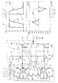
- an output buffer or off-chip driver circuit comprising in a per-se known way a high current capability CMOS inverter 1 made up of a P-channel MOSFET P1 (pull-up device) and by an N-channel MOSFET N1 (pull-down device) serially connected between a power supply line VDD and a ground line GND internal to the chip; the common node OUT of P1 and N1 represents an output buffer output signal, and is connected, through a respective package pin (not shown) to an external load impedance ZL on a printed circuit board (PCB).
- PCB printed circuit board
- An output buffer current slew rate control circuit comprises two circuit parts, one driving the pull-up device P1 (and therefore called pull-up control circuit part) and the other driving the pull-down device N1 (called for the same reason pull-down control circuit part).
- the two control circuit parts are dual.
- the pull-up control circuit part of the current slew rate control circuit comprises a bias network BIAS1 which supplies bias gate voltages BV3 and BV4 respectively to a P-channel MOSFET C3 and to an N-channel MOSFET C4 serially connected between the internal power supply line VDD and ground line GND; the common node 2 of C3 and C4 is connected to the gate of P1.
- the bias network BIAS1 is connected to the power supply line VDD through a P-channel MOSFET E3 and to the ground line GND through an N-channel MOSFET E4; the activation of the bias network BIAS1 is submitted to the activation of both E3 and E4.
- the gate of E4 is controlled by an output signal 5 of a Schmitt trigger ST1 whose input is connected to the node 2; the gate of E3 is controlled by an output signal 6 of a first stage S1 of a pre-driver circuit 7, substantially represented by a cascade of two CMOS inverters supplied by an input signal IN.
- a P-channel MOSFET P2 is connected between the power supply line VDD and the node 2, and has the gate controlled by an output signal 8 of a second stage S2 of the pre-driver circuit 7.
- node 2 is at a logic "1"
- the input signal of ST1 is a logic "1”
- the output signal 5 of ST2 is a logic "1”
- E4 is on.
- E3 is off and P2 is on; the bias network BIAS1 is deactivated, and the bias voltages BV3 and BV4 are pulled to the ground voltage value; this causes C4 to be off and C3 to be in the linear region.
- Node 2 is therefore connected to the power supply line VDD through both P2 and C3.
- the "1" to "0" transistion of the signal 6 causes E3 to be turned on and since E4 is also on the bias network BIAS1 is activated.
- bias voltages BV3 and BV4 bias C3 and C4 in the saturation region they therefore behaves substantially as constant current source and sink, respectively, and the gate capacitance Cg1 of P1 is discharged by an almost constant discharge current ID1 equal to the difference between the drain current I4 of C4 and the drain current I3 of C3.
- a P-channel MOSFET P2 is connected between the power supply line VDD and the node 2; two serially-connected N-channel MOSFETs N5 and N6 are connected between the node 2 and the ground line GND.
- the gate of N5 is controlled by the signal EN11, while the gates of P2 and N6 are controlled by a common signal 8'.
- the second circuit branch comprises a P-channel MOSFET P7 connected between the power supply line VDD and the drain of an N-channel MOSFET N8 with source connected to ground; the gate of P7 is connected to the common node between P5 and P6, in the other circuit branch; the common node 9 between P7 and N8 controls the gate of P6; the gate of N8 is instead connected to the gate of N7, in a current-mirror configuration.
- the node 9 is also connected to the ground line GND through the series of a P-channel MOSFET P8 and of an N-channel MOSFET N9; the gate of P8 is controlled by the signal EN11, while the gate of N9 is controlled by the signal 8'; the signal 8' represents the output signal of an inverter IN1 whose input signal EN12 is supplied by a pre-driver circuit (not shown); the signal EN12 is therefore equivalent to the signal 6 in Figure 1.
- the second circuit part is exactly the dual of the just described first circuit part, obtained by substituting N-channel MOSFETs with P-channel counterparts, and the connections to the VDD line with connections to the GND line.
- the pre-driver circuit drives the signal EN12 to a "0" logic state
- P5 is turned on, and the bias network BN1 becomes active
- N9 is also turned on, and the node 9 is therefore pulled toward ground, so that a finite current can start flowing through P7 and N8
- the current mirror N8, N7 causes a same current to flow in the other branch of BN1
- the gate voltage of N7 which coincides with the bias voltage BV4, stabilizes at a level that is indipendent from the power supply voltage value, and which tracks process variations
- the current flowing through N7 is mirrored into C4.
- C4 can be biased by the voltage BV4 into the saturation condition, and substantially behaves as a constant current sink; since moreover P2 has been turned off, while N5 is still in the off condition, the gate capacitance of P1 is discharged by the almost constant drain current of C4; by properly dimensioning C4, it is possible to achieve the desired slew rate for the output current IP1.
- the signal EN11 goes high, turning P4 and P8 off.
- the bias network BN1 is deactivated, and N3 is turned on, so that C4 is turned off; EN11 turns N5 on, so that the node 2 is connected to the ground line GND through two N-channel MOSFETs N5 and N6, which are now operated in the linear region.
- C4 is represented by an array of MOSFETs which can be parallely connected, for example by means of metal options which can be laser-cutted, to vary the discharge current ID1, and consequently the slew rate of IP1. Controlled current slew rate ranging from 2 mA/ns to 25 mA/ns can be obtained. If moreover each of the MOSFET constituting the current sink C4 is serially connected to a MOSFET switch, it is possible to change the current slew rate by means of digital control signals; this can be useful in special applications wherein an integrated circuit drives a signal bus swicthing from an high-speed condition to a low noise condition.
- the proposed control circuit does not introduce steady-state consumption, and can be designed to work with power supply values as low as 3 V.
- the chip area required by the proposed control circuit is also very small.
Landscapes
- Physics & Mathematics (AREA)
- Engineering & Computer Science (AREA)
- Computer Hardware Design (AREA)
- Computing Systems (AREA)
- General Engineering & Computer Science (AREA)
- Mathematical Physics (AREA)
- Logic Circuits (AREA)
- Electronic Switches (AREA)
Claims (6)
- Integrierte Schaltung zur Steuerung der Stromanstiegsgeschwindigkeit eines Ausgangspuffers, wobei der Ausgangspuffer (1) aufweist:wobei die Stromerzeugermittel aufweisen:ein erstes MOS-Transistormittel (P1, N1) zum Liefern eines Stromes (IOUT) an eine Lastimpedanz (ZL),Stromerzeugermittel (BIAS1, BIAS2, BN1, BN2, C1-C4) zum Erzeugen eines konstanten Stromes (ID1, IC1), die auf das Schalten eines Eingangssignales (IN) des Ausgangspuffers zwischen zwei Logikzuständen aktiviert werden, und die einen Steuereingang (2, 3) des ersten Transistormittels zum Treiben des ersten Transistormittels mit einer Treiberspannung (V2, V3) mit einer durch den konstanten Strom bestimmten Anstiegsgeschwindigkeit treiben;dadurch gekennzeichnet,ein mit dem Steuereingang (2, 3) des ersten Transistormittels verbundenes zweites Transistormittel (C1-C4) undein Vorspannungsschaltungsmittel (BIAS1, BIAS2; BN1, BN2), das nach Schalten des Eingangssignales (IN) des Ausgangspuffers aktiviert wird und eine an einen zweiten Steuereingang des zweiten Transistormittels (C1-C4) angelegte Vorspannung (BV1-BV4; BV1, BV4) erzeugt zum Vorspannen des zweiten Transistormittels (C1-C4) in einen Arbeitsbereich konstanten Stromes, wobei die Vorspannung im wesentlichen über Variationen der Versorgungsspannung (VDD) der integrierten Schaltung konstant bleibt, so daß der konstante Strom im wesentlichen unabhängig von der Versorgungsspannung ist;daß das erste Transistormittel (P1, N1) einen Hochziehtransistor (P1) und einen Herunterziehtransistor (N1) zum elektrischen Verbinden der Lastimpedanz (ZL) mit einer Spannungsversorgungsleitung (VDD) bzw. einer Masseleitung (GND) aufweist;daß das zweite Transistormittel (C1-C4) einen ersten Transistor (C4) und einen zweiten Transistor (C1) aufweist, die mit der Steuerelektrode (2, 3) des Hochzieh- bzw. Herunterziehtransistors verbunden sind;daß das Vorspannungsschaltungsmittel (BIAS1, BIAS2; BN1, BN2) eine erste Vorspannungsschaltung (BIAS1; BN1) und eine zweite Vorspannungsschaltung (BIAS2; BN2) aufweist zum Erzeugen einer ersten (BV4) bzw. einer zweiten Vorspannung (BV1), die an die Steuerelektrode des ersten bzw. zweiten Transistors angelegt werden;und daß Steuerschaltungsmittel (ST1, ST2, IST) vorgesehen sind zum Deaktivieren des Vorspannungsschaltungsmittels (BIAS1, BIAS2; BN1, BN2),wenn die Treiberspannung (V2, V3) des ersten Transistormittels (P1, N1) einen vorbestimmten Wert erreicht, wobei die Steuerschaltungsmittel einen ersten Schmitt-Trigger (ST1; IST) und einen zweiten Schmitt-Trigger (ST2; IST) aufweisen, die mit der Steuerelektrode (2, 3) des Hochzieh- bzw. des Herunterziehtransistors (P1, N1) verbunden sind zum Deaktivieren der ersten Vorspannungsschaltung (BIAS1; BN1), wenn die Treiberspannung (V2) des Hochziehtransistors (P1) einen ersten vorgeschriebenen Wert erreicht, bzw. die zweite Vorspannungsschaltung (BIAS2; BN2), wenn die Treiberspannung (V3) des Herunterziehtransistors (N1) einen zweiten vorgeschriebenen Wert erreicht.
- Schaltung nach Anspruch 1, dadurch gekennzeichnet,
daß die durch das Vorspannungsschaltungsmittel (BIAS1, BIAS2; BN1, BN2) erzeugte Vorspannung (BV1-BV4; BV1, BV4) so variiert, daß den Variationen elektrische Parameter der Komponenten des Vorspannungsschaltungsmittels aufgrund von Variationen im Herstellungsvorgang gefolgt wird. - Schaltung nach Anspruch 2, dadurch gekennzeichnet,
daß die erste Vorspannungsschaltung (BIAS1; BN1) und die zweite Vorspannungsschaltung (BIAS2; BN2) jeweils eine Bootstrap-Referenzspannungserzeugerschaltung aufweisen. - Schaltung nach Anspruch 3, dadurch gekennzeichnet,
daß die erste Vorspannungsschaltung (BIAS1; BN1) auf das Schalten hin des Eingangssignales (IN) von einem ersten Logikzustand zu einem zweiten Logikzustand aktiviert wird und die zweite Vorspannungsschaltung (BIAS2; BN2) auf das Schalten hin des Eingangssignales von dem zweiten Logikzustand zu dem ersten Logikzustand aktiviert wird. - Schaltung nach Anspruch 4, gekennzeichnet durch
einen durch das Eingangssignal (IN) getriebenen dritten Transistor (P2) zum elektrischen Verbinden der Steuerelektrode (2) des Hochziehtransistors (P1) mit einer Spannung geeignet zum Abschalten des letzteren auf das Schalten hin des Eingangssignales von dem zweiten Logikzustand zu dem ersten Logikzustand und einem durch das Eingangssignal getriebenen vierten Transistor (N2) zum elektrischen Verbinden der Steuerelektrode (3) des Herunterziehtransistors (N1) mit einer Spannung geeignet zum Abschalten des letzteren auf das Schalten hin des Eingangssignales von dem ersten Logikzustand zu dem zweiten Logikzustand. - Schaltung nach Anspruch 5, dadurch gekennzeichnet,
daß der Hochziehtransistor (P1), der zweite Transistor (C1) und der dritte Transistor (P2) P-Kanal-MOSFETs sind, während der Herunterziehtransistor (N1), der erste Transistor (C4) und der vierte Transistor (N2) N-Kanal-MOSFETs sind.
Priority Applications (4)
| Application Number | Priority Date | Filing Date | Title |
|---|---|---|---|
| EP94830190A EP0678983B1 (de) | 1994-04-22 | 1994-04-22 | Integrierte Schaltung zur Steuerung der Stromanstiegsgeschwindigkeit eines Ausgangspuffers |
| DE69412788T DE69412788T2 (de) | 1994-04-22 | 1994-04-22 | Integrierte Schaltung zur Steuerung der Stromanstiegsgeschwindigkeit eines Ausgangspuffers |
| US08/425,000 US5623216A (en) | 1994-04-22 | 1995-04-19 | Output buffer current slew rate control integrated circuit |
| JP7096827A JP2907752B2 (ja) | 1994-04-22 | 1995-04-21 | 出力バッファ電流スリューレート制御集積回路 |
Applications Claiming Priority (1)
| Application Number | Priority Date | Filing Date | Title |
|---|---|---|---|
| EP94830190A EP0678983B1 (de) | 1994-04-22 | 1994-04-22 | Integrierte Schaltung zur Steuerung der Stromanstiegsgeschwindigkeit eines Ausgangspuffers |
Publications (2)
| Publication Number | Publication Date |
|---|---|
| EP0678983A1 EP0678983A1 (de) | 1995-10-25 |
| EP0678983B1 true EP0678983B1 (de) | 1998-08-26 |
Family
ID=8218430
Family Applications (1)
| Application Number | Title | Priority Date | Filing Date |
|---|---|---|---|
| EP94830190A Expired - Lifetime EP0678983B1 (de) | 1994-04-22 | 1994-04-22 | Integrierte Schaltung zur Steuerung der Stromanstiegsgeschwindigkeit eines Ausgangspuffers |
Country Status (4)
| Country | Link |
|---|---|
| US (1) | US5623216A (de) |
| EP (1) | EP0678983B1 (de) |
| JP (1) | JP2907752B2 (de) |
| DE (1) | DE69412788T2 (de) |
Cited By (3)
| Publication number | Priority date | Publication date | Assignee | Title |
|---|---|---|---|---|
| US9461624B2 (en) | 2014-11-17 | 2016-10-04 | Infineon Technologies Ag | Output driver slew control |
| US10659051B1 (en) | 2019-05-10 | 2020-05-19 | Nxp Usa, Inc. | Bidirectional voltage translator with pulse width control |
| US11405037B2 (en) | 2020-12-18 | 2022-08-02 | Nxp B.V. | Driver circuit of voltage translator |
Families Citing this family (63)
| Publication number | Priority date | Publication date | Assignee | Title |
|---|---|---|---|---|
| US5926651A (en) * | 1995-07-28 | 1999-07-20 | Intel Corporation | Output buffer with current paths having different current carrying characteristics for providing programmable slew rate and signal strength |
| US5771389A (en) * | 1996-02-28 | 1998-06-23 | Intel Corporation | Low slew rate output buffer with staged biasing voltage |
| US5898315A (en) * | 1996-05-17 | 1999-04-27 | Cypress Semiconductor Corp. | Output buffer circuit and method having improved access |
| US5952817A (en) * | 1997-04-24 | 1999-09-14 | Linear Technology Corporation | Apparatus and method using waveform shaping for reducing high frequency noise from switching inductive loads |
| US5969554A (en) * | 1997-06-09 | 1999-10-19 | International Business Machines Corp. | Multi-function pre-driver circuit with slew rate control, tri-state operation, and level-shifting |
| US6040707A (en) * | 1997-09-15 | 2000-03-21 | Intersil Corporation | Constant slew rate amplifier |
| JP3076300B2 (ja) | 1998-04-20 | 2000-08-14 | 日本電気アイシーマイコンシステム株式会社 | 出力バッファ回路 |
| JPH11308087A (ja) * | 1998-04-24 | 1999-11-05 | Mitsubishi Electric Corp | スルーレートコントロール付き出力バッファ回路 |
| US6157204A (en) | 1998-08-05 | 2000-12-05 | Micron Technology, Inc. | Buffer with adjustable slew rate and a method of providing an adjustable slew rate |
| US6670822B2 (en) * | 1998-08-11 | 2003-12-30 | Fairchild Semiconductor Corporation | Transceiver driver with programmable edge rate control independent of fabrication process, supply voltage, and temperature |
| DE19910352C1 (de) * | 1999-03-09 | 2000-06-15 | Siemens Ag | Kompensationsschaltung für Treiberschaltungen |
| US6339351B1 (en) * | 1999-06-07 | 2002-01-15 | Sun Microsystems, Inc. | Output driver with improved impedance control |
| US6366139B1 (en) * | 1999-06-07 | 2002-04-02 | Sun Microsystems, Inc. | Method for an output driver with improved impedance control |
| US6278306B1 (en) * | 1999-06-07 | 2001-08-21 | Sun Microsystems, Inc. | Method for an output driver with improved slew rate control |
| US6281729B1 (en) * | 1999-06-07 | 2001-08-28 | Sun Microsystems, Inc. | Output driver with improved slew rate control |
| US6285215B1 (en) * | 1999-09-02 | 2001-09-04 | Micron Technology, Inc. | Output driver having a programmable edge rate |
| US6294924B1 (en) | 1999-09-20 | 2001-09-25 | Sun Microsystems, Inc. | Dynamic termination logic driver with improved slew rate control |
| US6316957B1 (en) | 1999-09-20 | 2001-11-13 | Sun Microsystems, Inc. | Method for a dynamic termination logic driver with improved impedance control |
| US6297677B1 (en) | 1999-09-20 | 2001-10-02 | Sun Microsystems, Inc. | Method for a dynamic termination logic driver with improved slew rate control |
| US6420913B1 (en) | 1999-09-20 | 2002-07-16 | Sun Microsystems, Inc. | Dynamic termination logic driver with improved impedance control |
| EP1091492A1 (de) | 1999-10-08 | 2001-04-11 | STMicroelectronics S.r.l. | Ausgangspuffer für digitale Signale |
| US6411120B1 (en) * | 2000-05-01 | 2002-06-25 | Macronix International Co., Ltd. | Output buffer drive circuit with initial drive for semiconductor devices |
| US6359484B1 (en) * | 2000-07-19 | 2002-03-19 | Exar Corporation | Slew-rate-control structure for high-frequency operation |
| DE60102759T2 (de) | 2000-08-07 | 2005-03-31 | Denso Corp., Kariya | Spannungsregler eines Kraftfahrzeugwechselstromgenerators |
| JP4212767B2 (ja) * | 2000-12-21 | 2009-01-21 | 旭化成エレクトロニクス株式会社 | 高速電流スイッチ回路および高周波電流源 |
| US6798237B1 (en) | 2001-08-29 | 2004-09-28 | Altera Corporation | On-chip impedance matching circuit |
| US6836144B1 (en) * | 2001-12-10 | 2004-12-28 | Altera Corporation | Programmable series on-chip termination impedance and impedance matching |
| US6812734B1 (en) | 2001-12-11 | 2004-11-02 | Altera Corporation | Programmable termination with DC voltage level control |
| US7109744B1 (en) | 2001-12-11 | 2006-09-19 | Altera Corporation | Programmable termination with DC voltage level control |
| US6535020B1 (en) * | 2001-12-18 | 2003-03-18 | Sun Microsystems, Inc. | Output buffer with compensated slew rate and delay control |
| JP3935925B2 (ja) * | 2002-03-04 | 2007-06-27 | 富士通株式会社 | 出力バッファ回路 |
| US6903588B2 (en) | 2003-04-15 | 2005-06-07 | Broadcom Corporation | Slew rate controlled output buffer |
| US6888369B1 (en) | 2003-07-17 | 2005-05-03 | Altera Corporation | Programmable on-chip differential termination impedance |
| US6888370B1 (en) | 2003-08-20 | 2005-05-03 | Altera Corporation | Dynamically adjustable termination impedance control techniques |
| US6859064B1 (en) | 2003-08-20 | 2005-02-22 | Altera Corporation | Techniques for reducing leakage current in on-chip impedance termination circuits |
| DE102004016978A1 (de) * | 2004-04-07 | 2005-06-30 | Infineon Technologies Ag | Ansteuerschaltung für einen Ausgangstreiber in einer integrierten Schaltung bzw. Treiberschaltung in einer integrierten Schaltung |
| JP2005321526A (ja) * | 2004-05-07 | 2005-11-17 | Renesas Technology Corp | 半導体集積回路装置、表示装置及びシステム |
| JP4500153B2 (ja) * | 2004-11-04 | 2010-07-14 | 旭化成エレクトロニクス株式会社 | 出力バッファ回路 |
| FR2879321B1 (fr) * | 2004-12-09 | 2007-03-02 | St Microelectronics Sa | Circuit de pilotage de bus |
| US7521975B2 (en) * | 2005-01-20 | 2009-04-21 | Advanced Micro Devices, Inc. | Output buffer with slew rate control utilizing an inverse process dependent current reference |
| US7218155B1 (en) | 2005-01-20 | 2007-05-15 | Altera Corporation | Techniques for controlling on-chip termination resistance using voltage range detection |
| US7221193B1 (en) | 2005-01-20 | 2007-05-22 | Altera Corporation | On-chip termination with calibrated driver strength |
| US7262637B2 (en) * | 2005-03-22 | 2007-08-28 | Micron Technology, Inc. | Output buffer and method having a supply voltage insensitive slew rate |
| US20060253663A1 (en) * | 2005-05-06 | 2006-11-09 | Micron Technology, Inc. | Memory device and method having a data bypass path to allow rapid testing and calibration |
| US7679397B1 (en) | 2005-08-05 | 2010-03-16 | Altera Corporation | Techniques for precision biasing output driver for a calibrated on-chip termination circuit |
| US7224187B2 (en) * | 2005-09-02 | 2007-05-29 | Winbond Electronics Corp. | CMOS buffer circuits and integrated circuits using the same |
| KR100668498B1 (ko) | 2005-11-09 | 2007-01-12 | 주식회사 하이닉스반도체 | 반도체 메모리의 데이터 출력장치 및 방법 |
| US7889609B2 (en) * | 2006-09-26 | 2011-02-15 | Silicon Core Technology, Inc. | Enhanced linearity DVD writing current circuit |
| WO2008085961A1 (en) * | 2007-01-05 | 2008-07-17 | Silicon Core Technology, Inc. | Higher performance dvd writing current circuit |
| US7449913B1 (en) * | 2007-06-20 | 2008-11-11 | Smartech Worldwide Limited | Pre-driver having slew-rate and crowbar-current controls for a CMOS output buffer |
| KR100906424B1 (ko) * | 2007-08-02 | 2009-07-09 | 한국과학기술원 | 출력 버퍼 및 이를 포함하는 전력 증폭기 |
| US7868622B2 (en) * | 2007-08-10 | 2011-01-11 | Seiko Instruments Inc. | Circuit for detecting power supply voltage drop |
| JP5031499B2 (ja) * | 2007-09-13 | 2012-09-19 | 株式会社リコー | 出力回路 |
| US7723153B2 (en) * | 2007-12-26 | 2010-05-25 | Organicid, Inc. | Printed organic logic circuits using an organic semiconductor as a resistive load device |
| JP5493291B2 (ja) * | 2008-05-12 | 2014-05-14 | セイコーエプソン株式会社 | 半導体装置および電子機器 |
| US8289302B2 (en) * | 2009-01-06 | 2012-10-16 | Himax Technologies Limited | Output buffer circuit with enhanced slew rate |
| CN102034540B (zh) * | 2009-09-27 | 2013-09-18 | 上海宏力半导体制造有限公司 | 压摆率控制装置及其控制方法 |
| US7969217B2 (en) * | 2009-10-13 | 2011-06-28 | Himax Technologies Limited | Output buffer with slew-rate enhancement output stage |
| CN102522991B (zh) | 2011-12-31 | 2014-05-21 | 开曼群岛威睿电通股份有限公司 | 采用三角积分调制的模拟数字转换器 |
| US9077514B1 (en) | 2014-01-28 | 2015-07-07 | Altera Corporation | Methods and structures for compensating and tracking process, voltage and temperature variations |
| US9473127B1 (en) * | 2015-07-06 | 2016-10-18 | Qualcomm Incorporated | Input/output (I/O) driver |
| US10181852B1 (en) | 2018-06-19 | 2019-01-15 | Nxp B.V. | Voltage translator with output slew rate control |
| TWI857447B (zh) * | 2022-12-30 | 2024-10-01 | 瑞昱半導體股份有限公司 | 充放電控制電路 |
Citations (1)
| Publication number | Priority date | Publication date | Assignee | Title |
|---|---|---|---|---|
| US4504779A (en) * | 1983-03-11 | 1985-03-12 | Hewlett-Packard Company | Electrical load drive and control system |
Family Cites Families (12)
| Publication number | Priority date | Publication date | Assignee | Title |
|---|---|---|---|---|
| US4612466A (en) * | 1984-08-31 | 1986-09-16 | Rca Corporation | High-speed output driver |
| JPH01161916A (ja) * | 1987-12-18 | 1989-06-26 | Toshiba Corp | 半導体集積回路 |
| US5051625B1 (en) * | 1988-10-28 | 1993-11-16 | Nissan Motor Co.,Ltd. | Output buffer circuits for reducing noise |
| US5021684A (en) * | 1989-11-09 | 1991-06-04 | Intel Corporation | Process, supply, temperature compensating CMOS output buffer |
| JP2598148B2 (ja) * | 1990-02-19 | 1997-04-09 | 富士通株式会社 | 出力回路 |
| US5017807A (en) * | 1990-07-05 | 1991-05-21 | At&T Bell Laboratories | Output buffer having capacitive drive shunt for reduced noise |
| JPH04175010A (ja) * | 1990-11-08 | 1992-06-23 | Nec Ic Microcomput Syst Ltd | 出力バッファ回路 |
| US5206544A (en) * | 1991-04-08 | 1993-04-27 | International Business Machines Corporation | CMOS off-chip driver with reduced signal swing and reduced power supply disturbance |
| EP0837562B1 (de) * | 1991-12-17 | 2001-07-04 | STMicroelectronics, Inc. | Ausgangspufferschaltung mit Vorladung |
| US5248906A (en) * | 1992-06-12 | 1993-09-28 | Advanced Micro Devices, Inc. | High speed CMOS output buffer circuit minimizes output signal oscillation and steady state current |
| GB9301934D0 (en) * | 1993-02-01 | 1993-03-17 | Immos Limited | Transistor switching |
| JP3175989B2 (ja) * | 1993-03-01 | 2001-06-11 | 株式会社東芝 | 出力バッファ回路 |
-
1994
- 1994-04-22 EP EP94830190A patent/EP0678983B1/de not_active Expired - Lifetime
- 1994-04-22 DE DE69412788T patent/DE69412788T2/de not_active Expired - Fee Related
-
1995
- 1995-04-19 US US08/425,000 patent/US5623216A/en not_active Expired - Lifetime
- 1995-04-21 JP JP7096827A patent/JP2907752B2/ja not_active Expired - Fee Related
Patent Citations (1)
| Publication number | Priority date | Publication date | Assignee | Title |
|---|---|---|---|---|
| US4504779A (en) * | 1983-03-11 | 1985-03-12 | Hewlett-Packard Company | Electrical load drive and control system |
Cited By (3)
| Publication number | Priority date | Publication date | Assignee | Title |
|---|---|---|---|---|
| US9461624B2 (en) | 2014-11-17 | 2016-10-04 | Infineon Technologies Ag | Output driver slew control |
| US10659051B1 (en) | 2019-05-10 | 2020-05-19 | Nxp Usa, Inc. | Bidirectional voltage translator with pulse width control |
| US11405037B2 (en) | 2020-12-18 | 2022-08-02 | Nxp B.V. | Driver circuit of voltage translator |
Also Published As
| Publication number | Publication date |
|---|---|
| DE69412788T2 (de) | 1999-04-29 |
| EP0678983A1 (de) | 1995-10-25 |
| JPH0856147A (ja) | 1996-02-27 |
| DE69412788D1 (de) | 1998-10-01 |
| US5623216A (en) | 1997-04-22 |
| JP2907752B2 (ja) | 1999-06-21 |
Similar Documents
| Publication | Publication Date | Title |
|---|---|---|
| US5623216A (en) | Output buffer current slew rate control integrated circuit | |
| US5021684A (en) | Process, supply, temperature compensating CMOS output buffer | |
| US4975598A (en) | Temperature, voltage, and process compensated output driver | |
| US6624672B2 (en) | Output buffer with constant switching current | |
| US5063308A (en) | Output driver with static and transient parts | |
| US6593795B2 (en) | Level adjustment circuit and data output circuit thereof | |
| US4777389A (en) | Output buffer circuits for reducing ground bounce noise | |
| US5034629A (en) | Output control circuit for reducing through current in CMOS output buffer | |
| EP0329285B1 (de) | Ausgangspuffer | |
| US6094086A (en) | High drive CMOS output buffer with fast and slow speed controls | |
| EP0493873A1 (de) | CMOS-Ausgangspufferschaltung mit reduzierten Prellen auf den Masseleitungen | |
| KR960011964B1 (ko) | 출력버퍼장치 | |
| JPH0334719A (ja) | 半導体集積回路 | |
| JPH04345317A (ja) | ドライバ回路、低ノイズドライバ回路及び低ノイズ低電圧スイングドライバ・レシーバ回路 | |
| US4810969A (en) | High speed logic circuit having feedback to prevent current in the output stage | |
| US5121000A (en) | Edge-rate feedback CMOS output buffer circuits | |
| US6617881B2 (en) | Semiconductor integrated circuit | |
| US6958626B2 (en) | Off chip driver | |
| US5708386A (en) | CMOS output buffer with reduced L-DI/DT noise | |
| EP0431624B1 (de) | Ausgangsschaltung mit grossem Stromsteuerungsvermögen ohne Erzeugung unerwünschter Spannungsschwankungen | |
| EP1454414B1 (de) | Schnelle ausgangsschaltung geeignet für geringe spannungen | |
| US6489815B2 (en) | Low-noise buffer circuit that suppresses current variation | |
| KR19980058197A (ko) | 제어신호를 이용한 출력패드 회로 | |
| US5254890A (en) | Ground bouncing reducing circuit and method | |
| JP3080718B2 (ja) | 出力バッファ回路 |
Legal Events
| Date | Code | Title | Description |
|---|---|---|---|
| PUAI | Public reference made under article 153(3) epc to a published international application that has entered the european phase |
Free format text: ORIGINAL CODE: 0009012 |
|
| AK | Designated contracting states |
Kind code of ref document: A1 Designated state(s): DE FR GB IT |
|
| 17P | Request for examination filed |
Effective date: 19960305 |
|
| 17Q | First examination report despatched |
Effective date: 19961126 |
|
| GRAG | Despatch of communication of intention to grant |
Free format text: ORIGINAL CODE: EPIDOS AGRA |
|
| GRAG | Despatch of communication of intention to grant |
Free format text: ORIGINAL CODE: EPIDOS AGRA |
|
| GRAH | Despatch of communication of intention to grant a patent |
Free format text: ORIGINAL CODE: EPIDOS IGRA |
|
| GRAH | Despatch of communication of intention to grant a patent |
Free format text: ORIGINAL CODE: EPIDOS IGRA |
|
| GRAA | (expected) grant |
Free format text: ORIGINAL CODE: 0009210 |
|
| AK | Designated contracting states |
Kind code of ref document: B1 Designated state(s): DE FR GB IT |
|
| RAP3 | Party data changed (applicant data changed or rights of an application transferred) |
Owner name: STMICROELECTRONICS S.R.L. |
|
| REF | Corresponds to: |
Ref document number: 69412788 Country of ref document: DE Date of ref document: 19981001 |
|
| ET | Fr: translation filed | ||
| PLBE | No opposition filed within time limit |
Free format text: ORIGINAL CODE: 0009261 |
|
| STAA | Information on the status of an ep patent application or granted ep patent |
Free format text: STATUS: NO OPPOSITION FILED WITHIN TIME LIMIT |
|
| 26N | No opposition filed | ||
| REG | Reference to a national code |
Ref country code: GB Ref legal event code: IF02 |
|
| PGFP | Annual fee paid to national office [announced via postgrant information from national office to epo] |
Ref country code: DE Payment date: 20030502 Year of fee payment: 10 |
|
| PG25 | Lapsed in a contracting state [announced via postgrant information from national office to epo] |
Ref country code: DE Free format text: LAPSE BECAUSE OF NON-PAYMENT OF DUE FEES Effective date: 20041103 |
|
| PGFP | Annual fee paid to national office [announced via postgrant information from national office to epo] |
Ref country code: FR Payment date: 20050408 Year of fee payment: 12 |
|
| PGFP | Annual fee paid to national office [announced via postgrant information from national office to epo] |
Ref country code: GB Payment date: 20050420 Year of fee payment: 12 |
|
| PG25 | Lapsed in a contracting state [announced via postgrant information from national office to epo] |
Ref country code: IT Free format text: LAPSE BECAUSE OF NON-PAYMENT OF DUE FEES;WARNING: LAPSES OF ITALIAN PATENTS WITH EFFECTIVE DATE BEFORE 2007 MAY HAVE OCCURRED AT ANY TIME BEFORE 2007. THE CORRECT EFFECTIVE DATE MAY BE DIFFERENT FROM THE ONE RECORDED. Effective date: 20050422 |
|
| PG25 | Lapsed in a contracting state [announced via postgrant information from national office to epo] |
Ref country code: GB Free format text: LAPSE BECAUSE OF NON-PAYMENT OF DUE FEES Effective date: 20060422 |
|
| GBPC | Gb: european patent ceased through non-payment of renewal fee |
Effective date: 20060422 |
|
| REG | Reference to a national code |
Ref country code: FR Ref legal event code: ST Effective date: 20061230 |
|
| PG25 | Lapsed in a contracting state [announced via postgrant information from national office to epo] |
Ref country code: FR Free format text: LAPSE BECAUSE OF NON-PAYMENT OF DUE FEES Effective date: 20060502 |