EP0679024A2 - Circuit avec un étage de réception haute fréquence et un étage de transmission - Google Patents
Circuit avec un étage de réception haute fréquence et un étage de transmission Download PDFInfo
- Publication number
- EP0679024A2 EP0679024A2 EP95200961A EP95200961A EP0679024A2 EP 0679024 A2 EP0679024 A2 EP 0679024A2 EP 95200961 A EP95200961 A EP 95200961A EP 95200961 A EP95200961 A EP 95200961A EP 0679024 A2 EP0679024 A2 EP 0679024A2
- Authority
- EP
- European Patent Office
- Prior art keywords
- frequency
- stage
- modulator
- splitter
- signal
- Prior art date
- Legal status (The legal status is an assumption and is not a legal conclusion. Google has not performed a legal analysis and makes no representation as to the accuracy of the status listed.)
- Granted
Links
- 230000005540 biological transmission Effects 0.000 title claims abstract description 16
- 239000013078 crystal Substances 0.000 claims abstract description 18
- 230000010355 oscillation Effects 0.000 abstract description 10
- 239000010453 quartz Substances 0.000 description 6
- VYPSYNLAJGMNEJ-UHFFFAOYSA-N silicon dioxide Inorganic materials O=[Si]=O VYPSYNLAJGMNEJ-UHFFFAOYSA-N 0.000 description 6
- 230000008878 coupling Effects 0.000 description 5
- 238000010168 coupling process Methods 0.000 description 5
- 238000005859 coupling reaction Methods 0.000 description 5
- 230000005236 sound signal Effects 0.000 description 3
- 230000003321 amplification Effects 0.000 description 1
- 238000003199 nucleic acid amplification method Methods 0.000 description 1
Images

Classifications
-
- H—ELECTRICITY
- H04—ELECTRIC COMMUNICATION TECHNIQUE
- H04N—PICTORIAL COMMUNICATION, e.g. TELEVISION
- H04N5/00—Details of television systems
- H04N5/44—Receiver circuitry for the reception of television signals according to analogue transmission standards
-
- H—ELECTRICITY
- H03—ELECTRONIC CIRCUITRY
- H03J—TUNING RESONANT CIRCUITS; SELECTING RESONANT CIRCUITS
- H03J5/00—Discontinuous tuning; Selecting predetermined frequencies; Selecting frequency bands with or without continuous tuning in one or more of the bands, e.g. push-button tuning, turret tuner
- H03J5/24—Discontinuous tuning; Selecting predetermined frequencies; Selecting frequency bands with or without continuous tuning in one or more of the bands, e.g. push-button tuning, turret tuner with a number of separate pretuned tuning circuits or separate tuning elements selectively brought into circuit, e.g. for waveband selection or for television channel selection
- H03J5/242—Discontinuous tuning; Selecting predetermined frequencies; Selecting frequency bands with or without continuous tuning in one or more of the bands, e.g. push-button tuning, turret tuner with a number of separate pretuned tuning circuits or separate tuning elements selectively brought into circuit, e.g. for waveband selection or for television channel selection used exclusively for band selection
Definitions
- the invention relates to a circuit arrangement with a high-frequency receiver stage (tuner) and a transmission stage (splitter) and a modulation arrangement (modulator) comprising transmission stage (splitter modulator).
- tuners and splitter modulators each require a crystal oscillator as a frequency reference.
- the object of the invention is to reduce the circuit complexity for a circuit arrangement which comprises both a tuner and a splitter modulator.
- this object is achieved by a circuit arrangement having a high-frequency reception stage (tuner) and a transmission stage (splitter) and a modulation arrangement (modulator) comprising a transmission stage (splitter-modulator), the signal division circuit (splitter) having a high-frequency signal input for supplying a high-frequency input signal, has a high-frequency signal output for outputting a high-frequency output signal, a first line for outputting the high-frequency input signal to the reception stage (tuner) and a second line for supplying a high-frequency output signal from the modulation arrangement (modulator), and wherein the reception stage (tuner) is set up for demodulating the high-frequency input signal and the modulation arrangement (modulator) for converting a baseband signal into the high-frequency output signal to be emitted by it, with devices for generating reference oscillations for the high-frequency reception stage (tuner) and the transmission stage (splitter modulator), these devices at least one for the high-
- the invention therefore provides to derive the frequency reference for both the tuner and the splitter modulator from a single quartz crystal or crystal oscillator.
- a crystal oscillator can thus be saved.
- the only crystal oscillator can then feed one oscillation generator (synthesizer) in the tuner and in the splitter modulator.
- the oscillating crystal or crystal oscillator of the tuner is also used by the splitter modulator.
- a transistor coupling stage can then preferably be inserted in the splitter modulator instead of the separate crystal oscillator between the oscillating crystal of the tuner and the oscillation generator, for example a phase-locked loop, of the splitter modulator. This transistor coupling stage allows the reference vibrations to be amplified and their low-impedance coupling into the vibration generator of the splitter modulator.
- the devices for generating reference vibrations have a phase-locked loop common to the high-frequency reception stage (tuner) and the transmission stage (splitter modulator).
- tuner high-frequency reception stage
- splitter modulator the transmission stage
- the effort is further reduced by the fact that only a single, common vibration generator is used for the combination of tuner and splitter modulator combined into one assembly. Only one quartz crystal, only one phase-locked loop and only one oscillator stage are required for this.
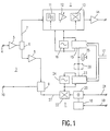
- Fig. 1 shows a combination of a tuner 1, a modulator 2 and a splitter 3, wherein the modulator 2 and splitter 3 together represent a transmission stage (splitter modulator).
- a high-frequency input signal for example a television signal from an antenna, can be fed to the splitter 3 via a high-frequency signal input 4.
- the high-frequency input signal reaches the tuner 1 from the first line 7, in which a frequency selection 11, an amplitude control 12 and a downward mixing 13 are carried out in the usual way by stages customary for this. Via an output amplifier 14 emitted an intermediate frequency signal.
- the stages 11 for the frequency selection and 13 for the downmixing are supplied in a conventional manner with reference vibrations from an oscillation generator assigned to the tuner 1, which comprises a phase-locked loop 15 and an oscillator stage 16.
- the phase-locked loop 15 can be controlled to tune the tuner 1 via control lines 17, preferably an I2C bus.
- the modulator 2 contains, in a manner known per se, an audio signal modulator 18 to which an audio baseband signal can be fed at an audio signal input 19 and which modulates it onto a sound carrier oscillation.
- the modulated audio signal is superimposed in a superposition stage 20 on a video baseband signal supplied via a video signal input 21.
- the combined baseband signal thus obtained is modulated in a baseband signal modulator stage 22 onto a high-frequency carrier oscillation which is generated in a vibration generator of the modulator 2, which comprises a second phase-locked loop 23 and a second oscillator stage 24.
- the oscillation generator 23, 24 of the modulator 2 has the same structure as that of the tuner 1.
- both oscillation generators 15, 16 and 23, 24 are controlled from a single oscillating crystal, with a transistor coupling stage 26 between the oscillating crystal 25 and the second phase-locked loop 23 can be arranged for vibration amplification and low-impedance coupling.
- a second line 27 feeds the high-frequency output signal of the modulator 2 to the second signal switch 9 of the splitter 3, via which it reaches the high-frequency signal output 10.
- the baseband signal modulator stage 22 of the modulator 2 is fed directly from the oscillator stage 16 of the oscillation generator of the tuner 1.
- a preferred application of these circuit arrangements is in high-frequency processing stages of video recorders.
Landscapes
- Engineering & Computer Science (AREA)
- Multimedia (AREA)
- Signal Processing (AREA)
- Transmitters (AREA)
- Superheterodyne Receivers (AREA)
- Input Circuits Of Receivers And Coupling Of Receivers And Audio Equipment (AREA)
Applications Claiming Priority (2)
| Application Number | Priority Date | Filing Date | Title |
|---|---|---|---|
| DE4413927 | 1994-04-21 | ||
| DE4413927 | 1994-04-21 |
Publications (3)
| Publication Number | Publication Date |
|---|---|
| EP0679024A2 true EP0679024A2 (fr) | 1995-10-25 |
| EP0679024A3 EP0679024A3 (fr) | 1996-10-16 |
| EP0679024B1 EP0679024B1 (fr) | 2000-03-01 |
Family
ID=6516081
Family Applications (1)
| Application Number | Title | Priority Date | Filing Date |
|---|---|---|---|
| EP95200961A Expired - Lifetime EP0679024B1 (fr) | 1994-04-21 | 1995-04-18 | Circuit avec un étage de réception haute fréquence et un modulateur pour transmission |
Country Status (4)
| Country | Link |
|---|---|
| US (1) | US5640688A (fr) |
| EP (1) | EP0679024B1 (fr) |
| JP (1) | JP3806160B2 (fr) |
| DE (2) | DE19509567A1 (fr) |
Cited By (1)
| Publication number | Priority date | Publication date | Assignee | Title |
|---|---|---|---|---|
| EP0769872A3 (fr) * | 1995-10-17 | 1997-05-02 | Philips Patentverwaltung GmbH | Circuit avec un étage de réception haute fréquence et un étage de transmission |
Families Citing this family (6)
| Publication number | Priority date | Publication date | Assignee | Title |
|---|---|---|---|---|
| JP3070442B2 (ja) * | 1995-05-24 | 2000-07-31 | 日本電気株式会社 | ディジタル変復調回路 |
| JPH1013181A (ja) * | 1996-06-21 | 1998-01-16 | Nec Corp | Ifフィルタ自動整合方式 |
| DE19813666A1 (de) * | 1998-03-27 | 1999-09-30 | Grundig Ag | Fernsehgerät mit HF-Signalaufspaltung innerhalb des Tuners |
| GB9905836D0 (en) * | 1999-03-15 | 1999-05-05 | Pace Micro Tech Ltd | Amplitude control for tv broadcast systems |
| JP3068081U (ja) | 1999-10-08 | 2000-04-21 | 船井電機株式会社 | 発振信号処理装置 |
| DE10300892A1 (de) * | 2003-01-13 | 2004-07-22 | Deutsche Thomson-Brandt Gmbh | Schaltbares abstimmbares Bandfilter mit optimiertem Frequenzgang |
Family Cites Families (9)
| Publication number | Priority date | Publication date | Assignee | Title |
|---|---|---|---|---|
| GB1524183A (en) * | 1975-11-05 | 1978-09-06 | Communications Patents Ltd | Video cassette recorders |
| JPS54127209A (en) * | 1978-03-27 | 1979-10-03 | Hitachi Denshi Ltd | Structure system of radio equipment |
| GB2064271B (en) * | 1979-07-06 | 1983-09-28 | Plessey Co Ltd | Transceivers |
| US4521916A (en) * | 1983-11-29 | 1985-06-04 | Rca Corporation | Frequency synthesis tuning control system for a double-conversion tuner |
| US4660182A (en) * | 1984-06-20 | 1987-04-21 | The Unites States Of America As Represented By The Secretary Of The Navy | Programmable multichannel sonobuoy transmitter |
| JPS61230484A (ja) * | 1985-04-04 | 1986-10-14 | Alps Electric Co Ltd | Catvコンバ−タ |
| DE3728381A1 (de) * | 1987-08-26 | 1989-03-09 | Thomson Brandt Gmbh | Schaltungsanordnung zur verteilung eines antennensignals |
| FR2630873B1 (fr) * | 1988-04-29 | 1991-04-12 | Ixea | Procedes pour transmettre des signaux video, cameras video pour cette transmission et applications de ces cameras |
| FI91819C (fi) * | 1991-11-05 | 1994-08-10 | Nokia Mobile Phones Ltd | Menetelmä kahden eri taajuusalueella toimivan digitaalisen radiopuhelimen taajuuksien muodostamiseksi |
-
1995
- 1995-03-16 DE DE19509567A patent/DE19509567A1/de not_active Withdrawn
- 1995-04-18 DE DE59507857T patent/DE59507857D1/de not_active Expired - Lifetime
- 1995-04-18 EP EP95200961A patent/EP0679024B1/fr not_active Expired - Lifetime
- 1995-04-19 JP JP09352395A patent/JP3806160B2/ja not_active Expired - Lifetime
- 1995-04-20 US US08/426,294 patent/US5640688A/en not_active Expired - Lifetime
Cited By (2)
| Publication number | Priority date | Publication date | Assignee | Title |
|---|---|---|---|---|
| EP0769872A3 (fr) * | 1995-10-17 | 1997-05-02 | Philips Patentverwaltung GmbH | Circuit avec un étage de réception haute fréquence et un étage de transmission |
| US5867771A (en) * | 1995-10-17 | 1999-02-02 | U.S. Philips Corporation | Circuit arrangement comprising a tuner and a splitter-modulator |
Also Published As
| Publication number | Publication date |
|---|---|
| DE59507857D1 (de) | 2000-04-06 |
| JP3806160B2 (ja) | 2006-08-09 |
| EP0679024B1 (fr) | 2000-03-01 |
| EP0679024A3 (fr) | 1996-10-16 |
| US5640688A (en) | 1997-06-17 |
| JPH0832882A (ja) | 1996-02-02 |
| DE19509567A1 (de) | 1995-10-26 |
Similar Documents
| Publication | Publication Date | Title |
|---|---|---|
| DE69832620T2 (de) | Empfänger mit mehreren Tunern | |
| EP0438075B1 (fr) | Système optique de transmission de télévision par câble | |
| DE1416141B2 (de) | Verfahren und anordnung zur stereophonischen tonuebertragung | |
| DE69023206T2 (de) | Relaisübertragungssystem. | |
| EP0073420B1 (fr) | Etage de réception pour des récepteurs radio et télévision | |
| EP0679024A2 (fr) | Circuit avec un étage de réception haute fréquence et un étage de transmission | |
| EP0769872B1 (fr) | Circuit avec un étage de réception haute fréquence et un étage de transmission | |
| AT259624B (de) | Sendevorrichtung zur Übertragung amplitudenmodulierter Schwingungen | |
| DE69801358T2 (de) | Frequenzwandlerschaltung für Kabelempfänger mit Modem | |
| US4794458A (en) | Modulation device | |
| EP0304611B1 (fr) | Montage de circuits pour la distribution de signaux d'antenne | |
| KR100240306B1 (ko) | Rf 변조기 및 tv 튜너를 구비하는 고주파기기 | |
| DE845219C (de) | Anordnung zur Mehrkanaluebertragung von Signalen mittels frequenzmodulierter Traegerwellen | |
| DE69222279T2 (de) | TDMA-TDD Sender-Empfänger | |
| DE19513005A1 (de) | Einrichtung zum Hörfunkempfang und zur Anzeige und Verwertung von Informationen aus dem Hörfunk | |
| DE2904565A1 (de) | Mehrnormen-fernsehempfangsgeraet | |
| DE3420338A1 (de) | Superheterodyn-radio-sende- und empfangsvorrichtung | |
| DE19758762B4 (de) | Drahtloses Informationszugriffssystem | |
| DE1082306B (de) | Schaltungsanordnung fuer Raum-Diversity-Empfang | |
| DE2645567C2 (de) | Schaltungsanordnung zur automatischen Abstimmsteuerung eines Fernsehempfängers | |
| DE2941712C2 (fr) | ||
| DE1416141C (fr) | ||
| KR920001479Y1 (ko) | 케이블 텔레비젼 튜너의 비트 잡음 제거회로 | |
| AT237036B (de) | Frequenzmodulator | |
| DE1034213B (de) | Sendeanordnung fuer die UEbertragung des Bild- und Tonkanals eines Fernsehsenders |
Legal Events
| Date | Code | Title | Description |
|---|---|---|---|
| PUAI | Public reference made under article 153(3) epc to a published international application that has entered the european phase |
Free format text: ORIGINAL CODE: 0009012 |
|
| AK | Designated contracting states |
Kind code of ref document: A2 Designated state(s): DE FR GB |
|
| PUAL | Search report despatched |
Free format text: ORIGINAL CODE: 0009013 |
|
| AK | Designated contracting states |
Kind code of ref document: A3 Designated state(s): DE FR GB |
|
| 17P | Request for examination filed |
Effective date: 19970416 |
|
| 17Q | First examination report despatched |
Effective date: 19981104 |
|
| GRAG | Despatch of communication of intention to grant |
Free format text: ORIGINAL CODE: EPIDOS AGRA |
|
| GRAG | Despatch of communication of intention to grant |
Free format text: ORIGINAL CODE: EPIDOS AGRA |
|
| GRAH | Despatch of communication of intention to grant a patent |
Free format text: ORIGINAL CODE: EPIDOS IGRA |
|
| GRAH | Despatch of communication of intention to grant a patent |
Free format text: ORIGINAL CODE: EPIDOS IGRA |
|
| RAP3 | Party data changed (applicant data changed or rights of an application transferred) |
Owner name: KONINKLIJKE PHILIPS ELECTRONICS N.V. Owner name: PHILIPS CORPORATE INTELLECTUAL PROPERTY GMBH |
|
| GRAA | (expected) grant |
Free format text: ORIGINAL CODE: 0009210 |
|
| AK | Designated contracting states |
Kind code of ref document: B1 Designated state(s): DE FR GB |
|
| REF | Corresponds to: |
Ref document number: 59507857 Country of ref document: DE Date of ref document: 20000406 |
|
| GBT | Gb: translation of ep patent filed (gb section 77(6)(a)/1977) |
Effective date: 20000503 |
|
| ET | Fr: translation filed | ||
| PLBE | No opposition filed within time limit |
Free format text: ORIGINAL CODE: 0009261 |
|
| STAA | Information on the status of an ep patent application or granted ep patent |
Free format text: STATUS: NO OPPOSITION FILED WITHIN TIME LIMIT |
|
| 26N | No opposition filed | ||
| REG | Reference to a national code |
Ref country code: GB Ref legal event code: IF02 |
|
| REG | Reference to a national code |
Ref country code: GB Ref legal event code: 746 Effective date: 20021025 |
|
| REG | Reference to a national code |
Ref country code: FR Ref legal event code: D6 |
|
| REG | Reference to a national code |
Ref country code: GB Ref legal event code: 732E |
|
| REG | Reference to a national code |
Ref country code: FR Ref legal event code: TP |
|
| REG | Reference to a national code |
Ref country code: GB Ref legal event code: 732E Free format text: REGISTERED BETWEEN 20121108 AND 20121114 |
|
| REG | Reference to a national code |
Ref country code: DE Ref legal event code: R082 Ref document number: 59507857 Country of ref document: DE Representative=s name: MUELLER-BORE & PARTNER PATENTANWAELTE, EUROPEA, DE |
|
| REG | Reference to a national code |
Ref country code: DE Ref legal event code: R082 Ref document number: 59507857 Country of ref document: DE Representative=s name: MUELLER-BORE & PARTNER PATENTANWAELTE PARTG MB, DE Effective date: 20130211 Ref country code: DE Ref legal event code: R082 Ref document number: 59507857 Country of ref document: DE Representative=s name: MUELLER-BORE & PARTNER PATENTANWAELTE, EUROPEA, DE Effective date: 20130211 Ref country code: DE Ref legal event code: R081 Ref document number: 59507857 Country of ref document: DE Owner name: CALLAHAN CELLULAR L.L.C., WILMINGTON, US Free format text: FORMER OWNER: NXP B.V., EINDHOVEN, NL Effective date: 20130211 Ref country code: DE Ref legal event code: R081 Ref document number: 59507857 Country of ref document: DE Owner name: CALLAHAN CELLULAR L.L.C., US Free format text: FORMER OWNER: NXP B.V., EINDHOVEN, NL Effective date: 20130211 |
|
| REG | Reference to a national code |
Ref country code: FR Ref legal event code: TP Owner name: CALLAHAN CELLULAR L.L.C., US Effective date: 20130724 |
|
| PGFP | Annual fee paid to national office [announced via postgrant information from national office to epo] |
Ref country code: GB Payment date: 20140325 Year of fee payment: 20 |
|
| PGFP | Annual fee paid to national office [announced via postgrant information from national office to epo] |
Ref country code: FR Payment date: 20140328 Year of fee payment: 20 Ref country code: DE Payment date: 20140430 Year of fee payment: 20 |
|
| REG | Reference to a national code |
Ref country code: DE Ref legal event code: R071 Ref document number: 59507857 Country of ref document: DE |
|
| REG | Reference to a national code |
Ref country code: DE Ref legal event code: R071 Ref document number: 59507857 Country of ref document: DE |
|
| REG | Reference to a national code |
Ref country code: GB Ref legal event code: PE20 Expiry date: 20150417 |
|
| PG25 | Lapsed in a contracting state [announced via postgrant information from national office to epo] |
Ref country code: GB Free format text: LAPSE BECAUSE OF EXPIRATION OF PROTECTION Effective date: 20150417 |