EP0679952A2 - Elektrophotographische Aufzeichnungsmethode, bei der amorphes Silizium photoleitfähiges Material verwendet wird - Google Patents
Elektrophotographische Aufzeichnungsmethode, bei der amorphes Silizium photoleitfähiges Material verwendet wird Download PDFInfo
- Publication number
- EP0679952A2 EP0679952A2 EP95302783A EP95302783A EP0679952A2 EP 0679952 A2 EP0679952 A2 EP 0679952A2 EP 95302783 A EP95302783 A EP 95302783A EP 95302783 A EP95302783 A EP 95302783A EP 0679952 A2 EP0679952 A2 EP 0679952A2
- Authority
- EP
- European Patent Office
- Prior art keywords
- photosensitive material
- image
- toner
- amorphous silicon
- developing
- Prior art date
- Legal status (The legal status is an assumption and is not a legal conclusion. Google has not performed a legal analysis and makes no representation as to the accuracy of the status listed.)
- Granted
Links
Images


Classifications
-
- G—PHYSICS
- G03—PHOTOGRAPHY; CINEMATOGRAPHY; ANALOGOUS TECHNIQUES USING WAVES OTHER THAN OPTICAL WAVES; ELECTROGRAPHY; HOLOGRAPHY
- G03G—ELECTROGRAPHY; ELECTROPHOTOGRAPHY; MAGNETOGRAPHY
- G03G5/00—Recording-members for original recording by exposure, e.g. to light, to heat or to electrons; Manufacture thereof; Selection of materials therefor
- G03G5/02—Charge-receiving layers
- G03G5/04—Photoconductive layers; Charge-generation layers or charge-transporting layers; Additives therefor; Binders therefor
- G03G5/08—Photoconductive layers; Charge-generation layers or charge-transporting layers; Additives therefor; Binders therefor characterised by the photoconductive material being inorganic
- G03G5/082—Photoconductive layers; Charge-generation layers or charge-transporting layers; Additives therefor; Binders therefor characterised by the photoconductive material being inorganic and not being incorporated in a bonding material, e.g. vacuum deposited
- G03G5/08214—Silicon-based
-
- G—PHYSICS
- G03—PHOTOGRAPHY; CINEMATOGRAPHY; ANALOGOUS TECHNIQUES USING WAVES OTHER THAN OPTICAL WAVES; ELECTROGRAPHY; HOLOGRAPHY
- G03G—ELECTROGRAPHY; ELECTROPHOTOGRAPHY; MAGNETOGRAPHY
- G03G5/00—Recording-members for original recording by exposure, e.g. to light, to heat or to electrons; Manufacture thereof; Selection of materials therefor
- G03G5/005—Materials for treating the recording members, e.g. for cleaning, reactivating, polishing
Definitions
- the present invention relates to an electrophotographic method using an amorphous silicon photosensitive material. More particularly, the invention relates to an electrophotographic method which enables the life of the photosensitive material to be lengthened without permitting image to flow and makes it possible to stably obtain image for extended periods of time.
- amorphous silicon photosensitive material has been extensively used for electrophotography.
- the amorphous silicon (a-Si) photosensitive material exhibits high sensitivity on the side of long wavelengths and further gives such advantages as excellent surface rigidity and abrasion resistance.
- Japanese Laid-Open Patent Publication No. 15154/1986 discloses polishing an amorphous silicon photosensitive material by using, as a toner for the amorphous silicon photosensitive material, the one obtained by adding, to the surfaces of the toner, silicon carbide having an average particle diameter of from 0.1 to 1 ⁇ m in an amount of from 0.005 to 5% by weight based on the toner.
- Polishing the surface of the amorphous silicon photosensitive material is surely effective in preventing the flow of image.
- the surface is excessively polished, the charging performance is impaired and the life of the photosensitive material is shortened.
- the amount of polishing is small, on the other hand, the image tends to flow making it difficult to stably form the image.
- the present inventors have discovered the fact that the flow of image can be effectively prevented when in the amorphous silicon photosensitive material, the degree of oxidation in the drum (the photosensitive material) surface and the degree of deposition of discharge products establish a predetermined relationship.
- the object of the present invention therefore is to provide an electrophotographic method by using an amorphous silicon photosensitive material, which enables the life of the photosensitive material to be lengthened without permitting image to flow and makes it possible to stably obtain image for extended periods of time.
- an electrophotographic method using an amorphous silicon photosensitive material which comprises mainly charging, exposing to image-bearing light, developing, charging before transfer, transferring and cleaning, wherein in such a condition that satisfy the following relations (1) and (2): x ⁇ 30 (1) y ⁇ a ⁇ exp(-bx) (2) wherein x indicates a degree of oxidation in the surface of the photosensitive material (SiO/SiC), y indicates an amount of deposition of a discharge product generated by charging (mole/cm2), a is a number 2.2 x 10 ⁇ 9, and b is a number 2.0. an atmosphere around the photosensitive material is controlled and a surface of the photosensitive material is polished by the developing and the cleaning.
- ozone which is generating during the main charging and during the charging before transfer is exhausted, and that surfaces of the photosensitive material are polished by using a toner blended with a polishing agent.
- the image flow can be prevented without the need of exhausting the atmosphere in which the photosensitive material is placed to an excess degree or without the need of polishing the surface of the photosensitive material to an excess degree. Therefore, the life of the photosensitive material is not shortened and great advantage is obtained in cost. According to the present invention, for instance, favorable image without image flow can be stably obtained up to more than 100,000 pieces of copies and, particularly, up to more than 1,000,000 pieces of copies.
- the present inventors have studied the cause of image flow that occurs in the electrophotographic method using amorphous silicon photosensitive material and have postulated that the surface of the drum is oxidized with ozone, the surface layer becomes electrically conducting when it absorbs water in excess amounts, and electrically conducting property is promoted when the discharge products dissolve in the water.
- a representative amorphous silicon photosensitive material 31 that is generally used has an amorphous silicon photosensitive layer 3 formed on an electrically conducting substrate (aluminum drum) 32 in a state where it has not been used.
- the photosensitive layer 33 comprises a body (intermediate layer) 34 of -Si:H:B, a surface layer 35 of a-SiC:H, and a lower layer 36 of a-Si:H:B:O.
- ozone (O3) generated by electric discharge oxidizes the surface of the drum as represented by the following formula (3) O3 + Si ⁇ O2 + O + Si ⁇ O2 + SiO
- SiO on the surface of the drum exhibits high hygroscopic property and absorbs water, so that the surface exhibits adsorptive property.
- Fig. 1(D) illustrating the process of adsorbing discharge products
- products formed by corona discharge i.e., NOx, SOx, NH3 and the like dissolve in the water in the surface of the drum causing the electrically conducting property to be enhanced.
- the present inventors have estimated that the degree of oxidation (SiO/SiC)x in the surface of the amorphous silicon photosensitive material and the amount of deposition of discharge products (mol/cm2)y greatly affect the image flow, and have eagerly conducted experiments to obtain the following interesting results.
- the oxidation degree (SiO/SiC)x in the surface of the photosensitive material is a ratio of SiO and SiC in the surface of the photosensitive material found in compliance with ESCA (electron spectroscopy for chemical analysis, X-ray photoelectron spectroscopic method), and the amount of deposition of discharge products (mol/cm2)y is a value obtained by wiping off the surface of the photosensitive material with pure water and subjecting it to the ion chromatography.
- Fig. 2 is a graph plotting regions where image flow takes place, wherein the abscissa represents the degree of oxidation x in the surface of the photosensitive material and the ordinate represents the amount y of deposition of discharge products.
- Fig. 2 shows the following fact. That is, when the degree of oxidation (SiO/SiC)x is small in the surface of the photosensitive material, the allowable amount of deposition of discharge products (mol/cm2)y is relatively large. However, the allowable amount of deposition of discharge products (mol/cm2)y decreases with an increase in the degree of oxidation (SiO/SiC) in the surface of the photosensitive material.
- a corona charger is used for the main charging and for the charging before the transfer.
- ozone is generated but also other products such as NOx, SOx, NH3, etc. are generated due to corona discharge.
- Exhaust at the charging portion brings about double advantage; i.e., not only oxidation on the surface of the photosensitive material due to ozone is decreased but also deposition of the discharge products is prevented as well.
- the total ozone concentration in the drum surface is not higher than 6 ppm and, particularly, not higher than 1 ppm.
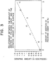
- Fig. 3 is a graph plotting a relationship between the blending amount of the polishing agent (% by weight) based on to the toner as represented by the abscissa and the scraping amount ( ⁇ /1000 pieces) of the surface of the photosensitive material as represented by the ordinate. It will be understood from Fig. 3 that the amount of scraping the oxide film on the surface of the photosensitive material can be adjusted by adjusting the amount of blending the polishing agent.
- the degree of oxidation (SiO/SiC)x in the surface of the photosensitive material is so maintained as will not be smaller than 0.4 even after more than 100,000 pieces of copies are obtained, and whereby the life of the photosensitive material is extended without much increasing the load for the electrophotographic apparatus, such as fans or electric power required therefor, and without losing electrophotographic properties of the photosensitive material such as charging potential.
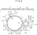
- an amorphous silicon photosensitive layer 2 is provided on the surface of the metal drum 1 that is driven.
- the drum is surrounded by a corona charger 3 for main charging; an image-exposing mechanism which includes a lamp 4, a transparent plate 5 for supporting the document and an optical system 6; a developing mechanism 8 having a developing agent 7; a corona charger 9 for charging before the transfer; a corona charger 10 for transferring the toner; a corona charger 11 for separating the paper; a discharging lamp 12; and a cleaning mechanism 13 in the order mentioned.
- a mechanism 14 for heating the photosensitive material 2 may be provided between the cleaning mechanism 13 and the corona charger 3 for main charging.
- the developing mechanism includes therein a developing agent stirrer mechanism 15, a developing sleeve 17 having a magnet 16 therein, and a hopper 18 for feeding developing toner.
- the hopper 18 for feeding developing toner contains the toner 19 to which the polishing agent is added, and feeds the toner 19 into the developing mechanism 8 using a toner feeding roll 20.
- the toner 19 fed into the developing mechanism 8 is mixed together with a magnetic carrier and is electrically charged to form a magnetic brush 21 on the developing sleeve 17, and is conveyed to a position of the photosensitive layer 2 where the magnetic brush 21 rubs the surface of the photosensitive layer 2 to develop the electrostatic latent image.
- a discharge mechanism comprising a discharge duct 22 is provided for the corona charger 3 for main charging and for the corona charger 9 for charging before the transfer and, as required, for the corona charger 10 for transferring the toner and/or the corona charger 11 for separating the paper.
- the photoconducting layer 2 is electrically charged by the corona charger 3 into a predetermined polarity (usually positive polarity). Then, a document 23 to be copied is illuminated with a lamp 4, and the a-Si photoconducting layer 2 is exposed to a light-ray image of the document through the optical system 6 thereby to form an electrostatic latent image that corresponds to the document image. The electrostatic latent image is visualized by the developing mechanism 8 to form a toner image.
- a predetermined polarity usually positive polarity
- the electric charge is removed by using the corona charger 9 for charging before the transfer.
- the electric charge is usually removed by using alternating current (AC) corona.
- Ozone is most likely to be generated during the charging by the corona charger 9 for charging before the transfer and, hence, it is particularly important to exhaust the atmosphere near the corona charger 9 for charging before the transfer.
- a transfer paper 24 is fed at a position of the charger 10 for transferring the toner so as to come into contact with the surface of the drum, and the corona charging of the same polarity as the electrostatic image is effected from the back surface of the transfer paper 24 to transfer the toner image onto the transfer paper 24.
- the transfer paper 24 onto which the toner image is transferred is electrostatically separated from the drum as the electric charge is removed by the corona charger 11 for separation, and is sent to a processing zone such as a fixing zone (not shown). After the toner is transferred, the residual electric charge in the photoconducting layer 2 is removed by being exposed over the whole surface to the light from the discharging lamp 12. The residual toner is then removed by the cleaning mechanism 13.
- any amorphous silicon photosensitive layer that has heretofore been known can be used.
- an amorphous silicon photosensitive layer that is precipitated on an electrically conducting substrate such as an aluminum blank tube by the plasma decomposition of a silane gas.
- the amorphous silicon photosensitive layer may be doped with hydrogen, halogen or the like, or may further be doped with an element of the Group III or the Group V of periodic table.
- the surface layer of the amorphous silicon photosensitive layer should exist in the form of SiC, and a three-layer structure shown in Fig. 1(A) is best suited.
- the whole thickness of the amorphous silicon photosensitive layer may range from 20 to 100 ⁇ m and, particularly, from 25 to 90 ⁇ m, and the thickness of the SiC surface layer may range from 0.2 to 1 ⁇ m and, particularly, from 0.3 to 0.8 ⁇ m.
- its thickness may range from 0.5 to 5 ⁇ m and, particularly, from 1 to 3 ⁇ m.
- a representative amorphous silicon photosensitive material has physical properties, i.e., dark electric conductivity of ⁇ 10 ⁇ 12 ⁇ 1 ⁇ cm ⁇ 1, activation energy of ⁇ 0.85 eV, photoelectric conductivity of > 10 ⁇ 7 ⁇ ⁇ 1 ⁇ cm ⁇ 1, optical band gap of 1.7 to 1.9 eV, and the amount of bonded hydrogen of 10 to 20 atomic %, and the film thereof has a dielectric constant of from 11.5 to 12.5.
- the amorphous silicon photosensitive material can be charged into positive polarity or negative polarity depending upon the kind of element with which it is doped. From the standpoint of decreasing as small as possible, the amount of ozone that is generated, however, it is desired that the amorphous silicon photosensitive material is charged into positive polarity. It is desired that the charged potential on the surface of the amorphous silicon photosensitive material is from 300 to 1000 volts and, particularly, from 400 to 900 volts. For this purpose, it is desired that the voltage applied to the corona charger for main charging is from 4 to 10 KV and, particularly, from 5 to 8 KV.
- the developing agent used for the electrophotography of the present invention will be a one-component-type magnetic developing agent or a two-component-type magnetic developing agent.
- the former developing agent there can be used any known developing agent in which the toner particles are blended with a magnetic powder and as the latter developing agent, there can be used any known developing agent comprising an electroscopic toner and a magnetic carrier.
- a coloring toner having electroscopic property and fixing property which generally comprises a granular composition having particle diameters of from 5 to 30 microns obtained by dispersing coloring pigments, charge control agents and the like in a binder resin.
- thermoplastic resin As the binder resin which is the toner component, there can be used a thermoplastic resin, or an uncured thermosetting resin or a thermosetting resin of an initial condensate.
- aromatic vinyl resin such as polystyrene, styrene/acrylic copolymer resin, acrylic resin, polyvinyl acetal resin, polyester resin, epoxy resin, phenol resin, petroleum resin, olefin resin, etc.
- coloring pigment there can be used carbon black, cadmium yellow, molybdenum orange, Pyrazolone Red, Fast Violet B, and Phthalocyanine Blue in one kind or in two or more kinds.
- an oil-soluble dye such as Nigrosine base (CI 50415), oil black (CI 26150), spiron black, metal complex salt dye, metal naphthenate, soap of a fatty acid metal, soap of resin acid, etc.
- the magnetic powder to be contained in the toner particles will be a widely known magnetic powder such as tri-iron tetroxide (magnetite), ferrites, magnetic metal, etc.
- the magnetic powder has an average particle diameter of generally from 0.1 to 10 ⁇ m and, particularly, from 0.1 to 1 ⁇ m. Furthermore, the content of the magnetic powder in the toner may be from 20 to 80% by weight and, particularly, from 30 to 60% by weight per the whole toner.
- the magnetic carrier used in combination with the toner will be any one of tri-iron tetroxide (magnetite), ferrites, iron powder or the like that has been widely known.
- the magnetic carrier has an average particle diameter of generally from 20 to 200 ⁇ m and, particularly, from 40 to 130 ⁇ m, and may further have a saturation magnetization of from 30 to 70 emu/g and, particularly, from 40 to 50 emu/g as measured at 50 KOe.
- the surfaces of the magnetic carrier have been coated with a resin.
- the optimum developing state can be maintained for extended periods of time and strikingly increased number of pieces of copies can be obtained.
- the resin for coating the magnetic carrier there can be used acrylic resin, styrene-acrylic resin, acryl-modified silicone resin, silicone resin, epoxy resin, rosin-modified phenol resin, formalin resin, cellulose resin, polyether resin, styrene-butadiene resin, polyurethane resin, polyvinyl formal resin, melamine resin, polycarbonate resin, and fluorine-containing resin such as ethylene tetrafluoride in one kind or in a combination of two or more kinds.
- the resin component is used in an amount of from 0.1 to 10 parts by weight and, particularly, from 0.2 to 5 parts by weight per 100 parts by weight of the carrier core material.
- the toner concentration may be so selected that the weight ratio of the carrier to the toner is from 99:1 to 90:10 and, particularly, from 98:2 to 94:6.
- polishing agents those known polishing agents having an average particle diameter of from 0.1 to 5 ⁇ m and, particularly, from 0.15 to 1 ⁇ m are preferably used. It is desired that these polishing agents have Mohs' hardness of generally from 5 to 10.
- polishing agent are not limited to the above-mentioned ones but further include oxide ceramics such as alumina (Al2O3), zirconia (ZrO2), mullite (3Al2O3 ⁇ 2SiO2), cordierite (2MgO/2Al2O3/5SiO2), titania (TiO2), steatite (MgO2 ⁇ SiO2), silica, silica alumina, and the like; carbide ceramics such as silicon carbide (SiC2), tungsten carbide (WC), zirconium carbide (ZrC), and the like; nitride ceramics such as boron nitride (BN), titanium nitride (TiN), silicon nitride (Si3N4) and the like; boride ceramics such as zirconium boride (ZrB2), titanium boride (TiB2) and the like; silicate ceramics such as tungsten silicate (WSi
- the amount of the polishing agent added to the toner varies depending upon the kind of the polishing agent and cannot be definitely determined but may, generally, be determined through experiment from the range of 0.1 to 10% by weight and, particularly, from the range of 0.5 to 5% by weight, so that an optimum scraping amount is obtained. That is, the relationship is found between the added amount of the polished agent and the scraping amount for each of the polishing agents as shown in Fig. 3, from which the amount of the polishing agent can be determined so that an optimum scraping amount (degree of oxidation in the surface of the photosensitive material) is obtained.
- Developing with the one-component-type developing agent or with the two-component-type developing agent can be carried out by using a magnetic brush.
- the developing may be effected under a condition where the magnetic brush is brought into intimate contact with the surface of the photosensitive material, or may be effected under a condition where there exists a tiny gap between the magnetic brush and the surface of the photosensitive material and the toner flies from the magnetic brush to the surface of the photosensitive material.
- a bias voltage for developing can be applied across the developing sleeve and the surface of the photosensitive drum.
- the bias voltage usually corresponds to a white-paper voltage of the photosensitive material, and is from about 50 to about 400 V in the case of the amorphous silicon photosensitive material.
- an AC voltage may be superposed to impart vibration to the toner.
- the electric charging before the transfer can be carried out by applying an AC voltage of, generally, 3 to 10 KV and, particularly, from 3.5 to 7 KV to the charger.
- the voltages applied to the charger for transferring the toner and to the charger for separating the transfer paper may lie within widely known ranges.
- the amount of deposition of discharge products on the surface of the photosensitive material can be considerably decreased by effecting the exhaust as described above, which, however, is greatly affected by another environmental factor, i.e., temperature near the surface of the photosensitive material. That is, the amount of deposition of discharge products decreases with an increase in the temperature on the surface of the photosensitive material.
- the temperature can generally be from 35 to 60 °C . Though not usually needed, it is allowable to provide a mechanism for heating the surface of the photosensitive material.
- the heating mechanism effectively works in preventing the flow of image caused by absorption of moisture in the earlier period of operation of the electrophotographic apparatus in which the temperature of the apparatus is low.
- the heating mechanism may be turned off when the temperature in the apparatus is raised, as a matter of course.
- the amount of deposition of discharge products on the surface of the photosensitive material affects the electric resistance of the surface of the photosensitive material.
- the surface resistance is detected and the heating mechanism 14 is turned on or off by providing a surface resistance sensor 25 and a temperature sensor 26 on the surface at an end of the photosensitive drum 2.
- the amount of discharge from the back surface of the corona chargers provided along the circumference of the photosensitive drum and the amount of the polishing agent blended in the toner were changed in a variety of ways. After 100,000 pieces of copies and 1,000,000 pieces of copies were obtained, the degree of oxidation (SiO/SiC) in the surface of the photosensitive drum and the amount of deposition of discharge products were measured according to the methods described above, and the flow of image was observed by naked eyes. The results were as shown in Table 1 and Fig. 2.
- Table 1 shows the results together with the amounts of the polishing agent added to the toner.
- Total ozone concentrations were found by inserting a tip of a hose in a gap between each of the chargers and the drum, the hose being connected to an ozone concentration meter, measuring the ozone concentrations at the portions where the chargers are provided, and adding them up together.
Landscapes
- Physics & Mathematics (AREA)
- General Physics & Mathematics (AREA)
- Chemical & Material Sciences (AREA)
- Inorganic Chemistry (AREA)
- Photoreceptors In Electrophotography (AREA)
- Developing Agents For Electrophotography (AREA)
- Electrostatic Charge, Transfer And Separation In Electrography (AREA)
Applications Claiming Priority (3)
| Application Number | Priority Date | Filing Date | Title |
|---|---|---|---|
| JP9170594 | 1994-04-28 | ||
| JP91705/94 | 1994-04-28 | ||
| JP9170594 | 1994-04-28 |
Publications (3)
| Publication Number | Publication Date |
|---|---|
| EP0679952A2 true EP0679952A2 (de) | 1995-11-02 |
| EP0679952A3 EP0679952A3 (de) | 1996-11-06 |
| EP0679952B1 EP0679952B1 (de) | 2001-01-10 |
Family
ID=14033936
Family Applications (1)
| Application Number | Title | Priority Date | Filing Date |
|---|---|---|---|
| EP95302783A Expired - Lifetime EP0679952B1 (de) | 1994-04-28 | 1995-04-25 | Elektrophotographische Aufzeichnungsmethode, bei der amorphes Silizium photoleitfähiges Material verwendet wird |
Country Status (3)
| Country | Link |
|---|---|
| US (1) | US5547805A (de) |
| EP (1) | EP0679952B1 (de) |
| DE (1) | DE69519815T2 (de) |
Cited By (2)
| Publication number | Priority date | Publication date | Assignee | Title |
|---|---|---|---|---|
| US5868782A (en) * | 1996-12-24 | 1999-02-09 | Global Therapeutics, Inc. | Radially expandable axially non-contracting surgical stent |
| EP0777164A3 (de) * | 1995-11-29 | 2001-02-14 | Kyocera Corporation | Elektrophotographisches Gerät |
Family Cites Families (7)
| Publication number | Priority date | Publication date | Assignee | Title |
|---|---|---|---|---|
| US4626487A (en) * | 1983-08-03 | 1986-12-02 | Canon Kabushiki Kaisha | Particulate developer containing inorganic scraper particles and image forming method using the same |
| JPH0629982B2 (ja) * | 1984-06-30 | 1994-04-20 | 三田工業株式会社 | 非晶質シリコン感光体用トナ− |
| US4764448A (en) * | 1985-04-05 | 1988-08-16 | Mitsubishi Chemical Industries, Ltd. | Amorphous silicon hydride photoreceptors for electrophotography, process for the preparation thereof, and method of use |
| JPH03197962A (ja) * | 1989-12-27 | 1991-08-29 | Konica Corp | 現像剤 |
| JP3195933B2 (ja) * | 1991-02-28 | 2001-08-06 | コニカ株式会社 | 静電像現像剤および画像形成方法 |
| JP3277213B2 (ja) * | 1991-12-30 | 2002-04-22 | 京セラ株式会社 | 画像形成方法 |
| US5319393A (en) * | 1992-04-02 | 1994-06-07 | Xerox Corporation | Multiple-spot beam control for a raster output scanner an electrophotographic printer |
-
1995
- 1995-04-24 US US08/427,174 patent/US5547805A/en not_active Expired - Lifetime
- 1995-04-25 EP EP95302783A patent/EP0679952B1/de not_active Expired - Lifetime
- 1995-04-25 DE DE69519815T patent/DE69519815T2/de not_active Expired - Lifetime
Cited By (2)
| Publication number | Priority date | Publication date | Assignee | Title |
|---|---|---|---|---|
| EP0777164A3 (de) * | 1995-11-29 | 2001-02-14 | Kyocera Corporation | Elektrophotographisches Gerät |
| US5868782A (en) * | 1996-12-24 | 1999-02-09 | Global Therapeutics, Inc. | Radially expandable axially non-contracting surgical stent |
Also Published As
| Publication number | Publication date |
|---|---|
| EP0679952A3 (de) | 1996-11-06 |
| DE69519815D1 (de) | 2001-02-15 |
| DE69519815T2 (de) | 2001-04-26 |
| US5547805A (en) | 1996-08-20 |
| EP0679952B1 (de) | 2001-01-10 |
Similar Documents
| Publication | Publication Date | Title |
|---|---|---|
| US7822351B2 (en) | Filling-rate lowering and rolling rate adjusting image forming apparatus | |
| EP0726503A2 (de) | Bilderzeugungsverfahren und -gerät | |
| KR0175117B1 (ko) | 전자 사진 장치 | |
| US6171742B1 (en) | Photosensitive member to be used for image-forming apparatus and image-forming apparatus comprising such photosensitive member | |
| EP0679952B1 (de) | Elektrophotographische Aufzeichnungsmethode, bei der amorphes Silizium photoleitfähiges Material verwendet wird | |
| EP0430703B1 (de) | Xerodruckverfahren | |
| JP3984860B2 (ja) | 現像剤担持体および該現像剤担持体を用いた現像装置およびプロセスカートリッジ | |
| US5963762A (en) | Electrophotographic apparatus performing image exposure and development simultaneously | |
| JP4035366B2 (ja) | 現像剤担持体、それを用いた現像装置及びプロセスカートリッジ | |
| JP2005010328A (ja) | 画像形成方法、画像形成装置、プロセスカートリッジ及び該画像形成装置に用いられる現像装置 | |
| JPH0816049A (ja) | アモルファス・シリコン感光体を用いる電子写真法 | |
| JPH11190916A (ja) | 画像形成方法 | |
| US5623716A (en) | Process for image forming using a photosensitive member having an amorphous carbon layer as an outermost surface layer | |
| JPH09269685A (ja) | 画像形成方法 | |
| US5732313A (en) | Charge apparatus and image forming apparatus | |
| EP0709747A2 (de) | Elektrofotografisches Verfahren, welches fotoempfindliches Material verwendet | |
| JP2001343773A (ja) | 電子写真用感光体及び電子写真装置 | |
| JP3984861B2 (ja) | 現像剤担持体及び該現像剤担持体を用いた現像装置及びプロセスカートリッジ | |
| JP3330008B2 (ja) | 電子写真装置 | |
| JP3330009B2 (ja) | 電子写真装置 | |
| JP3020698B2 (ja) | 画像形成装置 | |
| JP3152716B2 (ja) | 画像形成装置 | |
| JPH0629992B2 (ja) | 電子写真用二成分系現像剤 | |
| JPH0635341A (ja) | 電子写真法 | |
| JPS5811979A (ja) | トナ−画像の定着方法 |
Legal Events
| Date | Code | Title | Description |
|---|---|---|---|
| PUAI | Public reference made under article 153(3) epc to a published international application that has entered the european phase |
Free format text: ORIGINAL CODE: 0009012 |
|
| AK | Designated contracting states |
Kind code of ref document: A2 Designated state(s): DE FR GB IT |
|
| PUAL | Search report despatched |
Free format text: ORIGINAL CODE: 0009013 |
|
| AK | Designated contracting states |
Kind code of ref document: A3 Designated state(s): DE FR GB IT |
|
| 16A | New documents despatched to applicant after publication of the search report | ||
| 17P | Request for examination filed |
Effective date: 19970425 |
|
| 17Q | First examination report despatched |
Effective date: 19970623 |
|
| GRAG | Despatch of communication of intention to grant |
Free format text: ORIGINAL CODE: EPIDOS AGRA |
|
| GRAG | Despatch of communication of intention to grant |
Free format text: ORIGINAL CODE: EPIDOS AGRA |
|
| GRAH | Despatch of communication of intention to grant a patent |
Free format text: ORIGINAL CODE: EPIDOS IGRA |
|
| RAP1 | Party data changed (applicant data changed or rights of an application transferred) |
Owner name: KYOCERA MITA CORPORATION |
|
| GRAH | Despatch of communication of intention to grant a patent |
Free format text: ORIGINAL CODE: EPIDOS IGRA |
|
| GRAA | (expected) grant |
Free format text: ORIGINAL CODE: 0009210 |
|
| AK | Designated contracting states |
Kind code of ref document: B1 Designated state(s): DE FR GB IT |
|
| PG25 | Lapsed in a contracting state [announced via postgrant information from national office to epo] |
Ref country code: IT Free format text: LAPSE BECAUSE OF FAILURE TO SUBMIT A TRANSLATION OF THE DESCRIPTION OR TO PAY THE FEE WITHIN THE PRESCRIBED TIME-LIMIT;WARNING: LAPSES OF ITALIAN PATENTS WITH EFFECTIVE DATE BEFORE 2007 MAY HAVE OCCURRED AT ANY TIME BEFORE 2007. THE CORRECT EFFECTIVE DATE MAY BE DIFFERENT FROM THE ONE RECORDED. Effective date: 20010110 Ref country code: FR Free format text: LAPSE BECAUSE OF FAILURE TO SUBMIT A TRANSLATION OF THE DESCRIPTION OR TO PAY THE FEE WITHIN THE PRESCRIBED TIME-LIMIT Effective date: 20010110 |
|
| REF | Corresponds to: |
Ref document number: 69519815 Country of ref document: DE Date of ref document: 20010215 |
|
| EN | Fr: translation not filed | ||
| PLBE | No opposition filed within time limit |
Free format text: ORIGINAL CODE: 0009261 |
|
| STAA | Information on the status of an ep patent application or granted ep patent |
Free format text: STATUS: NO OPPOSITION FILED WITHIN TIME LIMIT |
|
| REG | Reference to a national code |
Ref country code: GB Ref legal event code: IF02 |
|
| 26N | No opposition filed | ||
| PGFP | Annual fee paid to national office [announced via postgrant information from national office to epo] |
Ref country code: DE Payment date: 20110420 Year of fee payment: 17 |
|
| PGFP | Annual fee paid to national office [announced via postgrant information from national office to epo] |
Ref country code: GB Payment date: 20110420 Year of fee payment: 17 |
|
| GBPC | Gb: european patent ceased through non-payment of renewal fee |
Effective date: 20120425 |
|
| PG25 | Lapsed in a contracting state [announced via postgrant information from national office to epo] |
Ref country code: GB Free format text: LAPSE BECAUSE OF NON-PAYMENT OF DUE FEES Effective date: 20120425 |
|
| REG | Reference to a national code |
Ref country code: DE Ref legal event code: R119 Ref document number: 69519815 Country of ref document: DE Effective date: 20121101 |
|
| PG25 | Lapsed in a contracting state [announced via postgrant information from national office to epo] |
Ref country code: DE Free format text: LAPSE BECAUSE OF NON-PAYMENT OF DUE FEES Effective date: 20121101 |