EP0680248B1 - Verfahren zur Herstellung einer elektronischen Leistungsschaltung und nach diesem Verfahren erhaltene elektronische Schaltung - Google Patents
Verfahren zur Herstellung einer elektronischen Leistungsschaltung und nach diesem Verfahren erhaltene elektronische Schaltung Download PDFInfo
- Publication number
- EP0680248B1 EP0680248B1 EP95400744A EP95400744A EP0680248B1 EP 0680248 B1 EP0680248 B1 EP 0680248B1 EP 95400744 A EP95400744 A EP 95400744A EP 95400744 A EP95400744 A EP 95400744A EP 0680248 B1 EP0680248 B1 EP 0680248B1
- Authority
- EP
- European Patent Office
- Prior art keywords
- components
- contact studs
- board
- circuit
- network
- Prior art date
- Legal status (The legal status is an assumption and is not a legal conclusion. Google has not performed a legal analysis and makes no representation as to the accuracy of the status listed.)
- Expired - Lifetime
Links
Images
Classifications
-
- H—ELECTRICITY
- H05—ELECTRIC TECHNIQUES NOT OTHERWISE PROVIDED FOR
- H05K—PRINTED CIRCUITS; CASINGS OR CONSTRUCTIONAL DETAILS OF ELECTRIC APPARATUS; MANUFACTURE OF ASSEMBLAGES OF ELECTRICAL COMPONENTS
- H05K3/00—Apparatus or processes for manufacturing printed circuits
- H05K3/30—Assembling printed circuits with electric components, e.g. with resistors
- H05K3/32—Assembling printed circuits with electric components, e.g. with resistors electrically connecting electric components or wires to printed circuits
- H05K3/34—Assembling printed circuits with electric components, e.g. with resistors electrically connecting electric components or wires to printed circuits by soldering
- H05K3/341—Surface mounted components
-
- H—ELECTRICITY
- H05—ELECTRIC TECHNIQUES NOT OTHERWISE PROVIDED FOR
- H05K—PRINTED CIRCUITS; CASINGS OR CONSTRUCTIONAL DETAILS OF ELECTRIC APPARATUS; MANUFACTURE OF ASSEMBLAGES OF ELECTRICAL COMPONENTS
- H05K1/00—Printed circuits
- H05K1/02—Details
- H05K1/0213—Electrical arrangements not otherwise provided for
- H05K1/0263—High current adaptations, e.g. printed high current conductors or using auxiliary non-printed means; Fine and coarse circuit patterns on one circuit board
-
- H—ELECTRICITY
- H05—ELECTRIC TECHNIQUES NOT OTHERWISE PROVIDED FOR
- H05K—PRINTED CIRCUITS; CASINGS OR CONSTRUCTIONAL DETAILS OF ELECTRIC APPARATUS; MANUFACTURE OF ASSEMBLAGES OF ELECTRICAL COMPONENTS
- H05K2201/00—Indexing scheme relating to printed circuits covered by H05K1/00
- H05K2201/10—Details of components or other objects attached to or integrated in a printed circuit board
- H05K2201/10007—Types of components
- H05K2201/1003—Non-printed inductor
-
- H—ELECTRICITY
- H05—ELECTRIC TECHNIQUES NOT OTHERWISE PROVIDED FOR
- H05K—PRINTED CIRCUITS; CASINGS OR CONSTRUCTIONAL DETAILS OF ELECTRIC APPARATUS; MANUFACTURE OF ASSEMBLAGES OF ELECTRICAL COMPONENTS
- H05K2201/00—Indexing scheme relating to printed circuits covered by H05K1/00
- H05K2201/10—Details of components or other objects attached to or integrated in a printed circuit board
- H05K2201/10227—Other objects, e.g. metallic pieces
- H05K2201/10272—Busbars, i.e. thick metal bars mounted on the printed circuit board [PCB] as high-current conductors
-
- H—ELECTRICITY
- H05—ELECTRIC TECHNIQUES NOT OTHERWISE PROVIDED FOR
- H05K—PRINTED CIRCUITS; CASINGS OR CONSTRUCTIONAL DETAILS OF ELECTRIC APPARATUS; MANUFACTURE OF ASSEMBLAGES OF ELECTRICAL COMPONENTS
- H05K2201/00—Indexing scheme relating to printed circuits covered by H05K1/00
- H05K2201/10—Details of components or other objects attached to or integrated in a printed circuit board
- H05K2201/10227—Other objects, e.g. metallic pieces
- H05K2201/1031—Surface mounted metallic connector elements
-
- H—ELECTRICITY
- H05—ELECTRIC TECHNIQUES NOT OTHERWISE PROVIDED FOR
- H05K—PRINTED CIRCUITS; CASINGS OR CONSTRUCTIONAL DETAILS OF ELECTRIC APPARATUS; MANUFACTURE OF ASSEMBLAGES OF ELECTRICAL COMPONENTS
- H05K2201/00—Indexing scheme relating to printed circuits covered by H05K1/00
- H05K2201/10—Details of components or other objects attached to or integrated in a printed circuit board
- H05K2201/10227—Other objects, e.g. metallic pieces
- H05K2201/10409—Screws
-
- H—ELECTRICITY
- H05—ELECTRIC TECHNIQUES NOT OTHERWISE PROVIDED FOR
- H05K—PRINTED CIRCUITS; CASINGS OR CONSTRUCTIONAL DETAILS OF ELECTRIC APPARATUS; MANUFACTURE OF ASSEMBLAGES OF ELECTRICAL COMPONENTS
- H05K2201/00—Indexing scheme relating to printed circuits covered by H05K1/00
- H05K2201/10—Details of components or other objects attached to or integrated in a printed circuit board
- H05K2201/10613—Details of electrical connections of non-printed components, e.g. special leads
- H05K2201/10954—Other details of electrical connections
- H05K2201/10962—Component not directly connected to the PCB
-
- H—ELECTRICITY
- H05—ELECTRIC TECHNIQUES NOT OTHERWISE PROVIDED FOR
- H05K—PRINTED CIRCUITS; CASINGS OR CONSTRUCTIONAL DETAILS OF ELECTRIC APPARATUS; MANUFACTURE OF ASSEMBLAGES OF ELECTRICAL COMPONENTS
- H05K3/00—Apparatus or processes for manufacturing printed circuits
- H05K3/22—Secondary treatment of printed circuits
- H05K3/222—Completing of printed circuits by adding non-printed jumper connections
-
- H—ELECTRICITY
- H05—ELECTRIC TECHNIQUES NOT OTHERWISE PROVIDED FOR
- H05K—PRINTED CIRCUITS; CASINGS OR CONSTRUCTIONAL DETAILS OF ELECTRIC APPARATUS; MANUFACTURE OF ASSEMBLAGES OF ELECTRICAL COMPONENTS
- H05K3/00—Apparatus or processes for manufacturing printed circuits
- H05K3/30—Assembling printed circuits with electric components, e.g. with resistors
- H05K3/32—Assembling printed circuits with electric components, e.g. with resistors electrically connecting electric components or wires to printed circuits
- H05K3/325—Assembling printed circuits with electric components, e.g. with resistors electrically connecting electric components or wires to printed circuits by abutting or pinching; Mechanical auxiliary parts therefor
-
- H—ELECTRICITY
- H05—ELECTRIC TECHNIQUES NOT OTHERWISE PROVIDED FOR
- H05K—PRINTED CIRCUITS; CASINGS OR CONSTRUCTIONAL DETAILS OF ELECTRIC APPARATUS; MANUFACTURE OF ASSEMBLAGES OF ELECTRICAL COMPONENTS
- H05K3/00—Apparatus or processes for manufacturing printed circuits
- H05K3/40—Forming printed elements for providing electric connections to or between printed circuits
- H05K3/4007—Surface contacts, e.g. bumps
- H05K3/4015—Surface contacts, e.g. bumps using auxiliary conductive elements, e.g. pieces of metal foil, metallic spheres
-
- Y—GENERAL TAGGING OF NEW TECHNOLOGICAL DEVELOPMENTS; GENERAL TAGGING OF CROSS-SECTIONAL TECHNOLOGIES SPANNING OVER SEVERAL SECTIONS OF THE IPC; TECHNICAL SUBJECTS COVERED BY FORMER USPC CROSS-REFERENCE ART COLLECTIONS [XRACs] AND DIGESTS
- Y02—TECHNOLOGIES OR APPLICATIONS FOR MITIGATION OR ADAPTATION AGAINST CLIMATE CHANGE
- Y02P—CLIMATE CHANGE MITIGATION TECHNOLOGIES IN THE PRODUCTION OR PROCESSING OF GOODS
- Y02P70/00—Climate change mitigation technologies in the production process for final industrial or consumer products
- Y02P70/50—Manufacturing or production processes characterised by the final manufactured product
Definitions
- the present invention relates to a method of manufacture of an electronic power circuit, as well than an electronic circuit obtained by this process.
- document EP-A-0 159 208 describes such a manufacturing process in which electronic components are laid flat and then soldered on a conductive network forming a previously printed circuit obtained from a metal plate, usually made of copper, placed on a good conductive material heat, for example aluminum, and between which is inserted a layer of insulating material of electricity.
- This structure provides a low thermal resistance between the core of electronic components for example of power and good material conductor of heat.
- the calories released by these power components can thus be transmitted to the heat conducting layer, and be removed by a cold source.
- the thickness of copper in the network conductor generally in a range from from 35 microns to 105 microns, the printed circuits do not cannot efficiently conduct current flow important necessary to supply circuits high power integrated.
- An object of the present invention is to provide a method of manufacturing an electronic circuit of power to overcome these drawbacks.
- Another object of the invention is to propose a method of manufacturing an electronic circuit power, easily automated and allowing mounting of components whose dimensions are incompatible with component assembly machines, and can not undergo a brazing operation.
- the subject of the present invention is a method of manufacturing an electronic circuit of power including components connected by soldering to connection locations of a conductive network a printed circuit board, in which the conductive network of the printed circuit depending on the circuit to be carried out, solder paste is placed on the network connection locations, we place on the plate of the first components intended to be fixed by soldering on network connection locations this, we place, on a part of the locations of connection of the plate network, connection pads of conductive material intended to receive second components to be placed on the plate after the brazing operation, we proceed to the operation of soldering of the first components and connection pads, and the second components are fixed on the pads of connection using mechanical fixing means, characterized in that the first components include integrated power circuits and second components have current bars connected to the plate by the connection pads.
- the invention also relates to a circuit power electronics produced by means of the manufacturing as defined above.
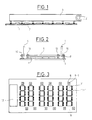
- Figure 1 shows an electronic circuit according to the prior art provided with connection elements allowing a large current to flow in parts of the plate.
- This circuit consists a printed circuit board 1 on which are soldered power components or integrated circuits 2 and a set of current bars 3 of which only one is shown in this figure. This bar is adapted to ensure a high power electrical connection between circuits 2 and external devices (not represented).
- Each current bar is mechanically clamped on the plate, at each of its ends, using screws and insulating barrels.
- connection locations for a printed circuit board connection pads on which different components are then fixed are then fixed.
- the term component here designates any element entering into the constitution of an electronic circuit, in particular integrated circuits, elements forming electrical or mechanical connection, etc ...
- FIG. 2 shows an example of realization of an electronic circuit provided with such pads.
- This circuit consists of a circuit plate printed 6 on which circuits have been soldered integrated 7 and connection pads 8.
- current 9 are fixed to the studs by mechanical means 10 such as screws. These bars are preferably sufficient dimensions to allow circulation in the large current flow plate, by example of the order of 300 A.
- the printed circuit board 6 receiving the components is formed in a known manner for example of a layer of conductive material, for example copper, deposited on a layer of good conductive material of the heat, for example aluminum, with interposition a layer of insulating material such as plastic film, between these layers.
- a layer of conductive material for example copper
- a layer of good conductive material of the heat for example aluminum
- a layer of insulating material such as plastic film
- solder paste is placed on connection locations of this conductive network for later connect during a brazing operation the components to the plate.
- connection locations are coated with solder, first components 11 (analogous to the components 7 described above) and for example of a housing 12, intended to be fixed by brazing on this one.
- These first components 11 are for example integrated power circuits placed on the network conductor so that their connection terminals 11-1 are in contact with solder paste on connection locations of this network, and that their housings are in direct contact with the layer of conductive material so as to dissipate the heat energy that they release when in operation.
- the installation of these first components on the plate can in known manner be produced by automatic machines.
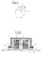
- FIG. 4 shows an example of realization of such a connection pad 8.
- This is of an element of conductive material, for example brass or copper, preferably in the shape of a parallelepiped, from 3 to 6 mm sides.
- this pad forms a square base with a side of 5 mm on which it rests, and a height of 6 mm. It has a hole 8-1 axial.
- This orifice can advantageously be tapped or self-tapping and be adapted to receive by example a screw.
- This stud is also covered with a layer of tinning material 5 microns thick to promote soldering.
- pads 8 can be placed on the plate printed circuit identical to that used for the first components, i.e. by means of a automatic component deposition machine.
- connection pads 8 After performing this soldering operation, second components are fixed by mechanical means on the connection pads 8. We thus connect to the plate during this step, all components that do not cannot be soldered due to their size incompatible with that of the oven, their structure does not allowing them to withstand the temperature of passage in the oven, or which would form a screen preventing the good soldering of the other components.
- connection pads 8 current bars 9 of sufficient size to allow circulation in the plate of fluxes important current.
- These current bars are provided, for example at near their ends, through holes through example of a screw 10 which enters hole 8-1 of the corresponding connection pad 8, so as to produce a mechanical and electrical connection of this bar on the plate through this pad.
- FIG. 5 shows a circuit electronics on which an electrical component such as transformer 13 has been attached to the circuit board printed after soldering using the method according to the invention.
- This transformer 13 consists of a winding 14 enclosed in a ferrite body 15. Characteristics ferrite magnets generally degrading at the irreversible heat, this transformer does not can be fixed on the plate by brazing in the oven.
- this transformer is then placed manually on the plate after passing it in the oven for the soldering of components and studs so that its carcass is in contact with the material layer driver of it.
- elements conductors 16 for example connection lugs supply terminals of this transformer, connection pads 8 so as to make a connection between this transformer and the printed circuit.
- This transformer is then kept in contact thermal, mechanical and electrical with the circuit printed.
- This method of producing a printed circuit power therefore achieves using of printed circuit boards on which a large number of types of components can be placed, any allowing them to be replaced easily.
Landscapes
- Engineering & Computer Science (AREA)
- Microelectronics & Electronic Packaging (AREA)
- Manufacturing & Machinery (AREA)
- Electric Connection Of Electric Components To Printed Circuits (AREA)
Claims (7)
- Verfahren zur Herstellung einer elektronischen Leistungsschaltung, die Komponenten aufweist, die durch Löten mit Verbindungsstellen eines leitenden Netzes einer gedruckten Schaltungsplatte (6) verbunden sind, bei dem das leitende Netz der gedruckten Schaltung in Abhängigkeit von der herzustellenden Schaltung gebildet wird, Lötpaste auf die Verbindungsstellen des Netzes aufgebracht wird, auf der Platte erste Komponenten (7, 11) angeordnet werden, die dazu bestimmt sind, durch Löten an Verbindungsstellen des Netzes derselben befestigt zu werden, auf einem Teil der Verbindungsstellen des Netzes der Platte Anschlußelemente (8) aus einem leitenden Material angebracht werden, die dazu bestimmt sind, zweite Komponenten (9; 13) aufzunehmen, die auf der Platte nach dem Lötverfahren angeordnet werden sollen, das Anlöten der ersten Komponenten (7, 11) und der Anschlußelemente (8) vorgenommen wird und die zweiten Komponenten (9; 13) an den Anschlußelementen mit Hilfe von mechanischen Befestigungsmitteln (10) befestigt werden, dadurch gekennzeichnet, daß die ersten Komponenten integrierte Leistungsschaltungen (7, 11) umfassen und die zweiten Komponenten Stromstäbe (9) umfassen, die mit der Platte durch die Anschlußelemente verbunden sind.
- Verfahren nach Anspruch 1, dadurch gekennzeichnet, daß die zweiten Komponenten ferner elektrische Komponenten (13) umfassen, die zwischen Anschlußelementen (8) angeordnet sind und die versehen sind mit Isolierflanschen (17), die mechanisch an den Elementen befestigt und derart ausgeführt sind, daß sie mechanisch diese Komponenten mit der Platte verbinden, sowie mit leitenden Elementen (16), die eine elektrische Verbindung zwischen den Anschlußelementen und diesen elektrischen Komponenten gewährleisten.
- Verfahren nach einem der Ansprüche 1 und 2, dadurch gekennzeichnet, daß die Anschlußelemente (8) die Form eines Parallelepipeds aufweisen, das mit einer Axialöffnung (8-1) für die Aufnahme der Befestigungsmittel der zweiten Komponenten versehen ist.
- Verfahren nach einem der Ansprüche 1 bis 3, dadurch gekennzeichnet, daß die Anschlußelemente mit einer verzinnten Schicht überzogen sind.
- Verfahren nach einem der Ansprüche 1 bis 4, bei dem eine Einkapselung der gedruckten Schaltung in einem dichten Kasten nach der Befestigung der zweiten Komponenten auf der Platte vorgenommen wird.
- Elektronische Leistungsschaltung, die mit Hilfe des Herstellungsverfahrens nach einem der Ansprüche 1 bis 5 hergestellt wurde, die eine gedruckte Schaltungsplatte (6) umfaßt, an deren Verbindungsstellen erste Komponenten und Anschlußelemente (8) angelötet sind, wobei die Anschlußelemente (8) zweite Komponenten mit den entsprechenden Verbindungsstellen verbinden, dadurch gekennzeichnet, daß die zweiten Komponenten Stromstäbe (9) umfassen.
- Elektronische Leistungsschaltung nach Anspruch 6, dadurch gekennzeichnet, daß die zweiten Komponenten ferner mindestens eine elektrische Komponente (13) umfassen.
Applications Claiming Priority (2)
| Application Number | Priority Date | Filing Date | Title |
|---|---|---|---|
| FR9404966A FR2719183B1 (fr) | 1994-04-25 | 1994-04-25 | Procédé de fabrication d'un circuit électronique de puissance et circuit électronique obtenu par ce procédé. |
| FR9404966 | 1994-04-25 |
Publications (2)
| Publication Number | Publication Date |
|---|---|
| EP0680248A1 EP0680248A1 (de) | 1995-11-02 |
| EP0680248B1 true EP0680248B1 (de) | 1999-03-10 |
Family
ID=9462485
Family Applications (1)
| Application Number | Title | Priority Date | Filing Date |
|---|---|---|---|
| EP95400744A Expired - Lifetime EP0680248B1 (de) | 1994-04-25 | 1995-04-03 | Verfahren zur Herstellung einer elektronischen Leistungsschaltung und nach diesem Verfahren erhaltene elektronische Schaltung |
Country Status (3)
| Country | Link |
|---|---|
| EP (1) | EP0680248B1 (de) |
| DE (1) | DE69508134T2 (de) |
| FR (1) | FR2719183B1 (de) |
Families Citing this family (2)
| Publication number | Priority date | Publication date | Assignee | Title |
|---|---|---|---|---|
| FR2803716B1 (fr) * | 2000-01-11 | 2002-04-05 | Sagem | Module electronique a composants de puissance et procede de fabrication |
| GB2545425B (en) * | 2015-12-14 | 2019-03-27 | Ge Aviat Systems Ltd | Distributed wiring board connections |
Family Cites Families (8)
| Publication number | Priority date | Publication date | Assignee | Title |
|---|---|---|---|---|
| FR2560437B1 (fr) * | 1984-02-28 | 1987-05-29 | Citroen Sa | Procede de report a plat d'elements de puissance sur un reseau conducteur par brasage de leurs connexions |
| GB8813233D0 (en) * | 1988-06-03 | 1988-07-06 | Amp Great Britain | Connecting electrical leads to electrical circuitry |
| US5065283A (en) * | 1990-06-12 | 1991-11-12 | Mitsubishi Denki Kabushiki Kaisha | Printed circuit board with busbar interconnections |
| JPH04341773A (ja) * | 1991-05-17 | 1992-11-27 | Mitsubishi Electric Corp | 端子台 |
| JP2827621B2 (ja) * | 1991-10-23 | 1998-11-25 | 三菱電機株式会社 | 大電流基板及びその製造方法 |
| DE9203941U1 (de) * | 1992-03-24 | 1992-05-07 | Schroff Gmbh, 7541 Straubenhardt | Vorrichtung zur Befestigung einer Stromschiene an einer Busplatine |
| DE9217684U1 (de) * | 1992-12-24 | 1993-02-25 | SL Elektronik Mechanik GmbH, 72336 Balingen | Klemme für eine Leiterplatte |
| DE9312961U1 (de) * | 1993-08-30 | 1993-11-18 | Karl Lumberg GmbH & Co, 58579 Schalksmühle | Elektrische Anschlußklemme für Leiterplatten |
-
1994
- 1994-04-25 FR FR9404966A patent/FR2719183B1/fr not_active Expired - Fee Related
-
1995
- 1995-04-03 EP EP95400744A patent/EP0680248B1/de not_active Expired - Lifetime
- 1995-04-03 DE DE69508134T patent/DE69508134T2/de not_active Expired - Fee Related
Also Published As
| Publication number | Publication date |
|---|---|
| FR2719183A1 (fr) | 1995-10-27 |
| DE69508134D1 (de) | 1999-04-15 |
| FR2719183B1 (fr) | 1996-07-12 |
| DE69508134T2 (de) | 1999-08-19 |
| EP0680248A1 (de) | 1995-11-02 |
Similar Documents
| Publication | Publication Date | Title |
|---|---|---|
| EP2801245B1 (de) | Vorrichtung zur montage von kondensatoren für einen elektronischen wandler | |
| FR2782597A1 (fr) | Module d'alimentation electrique | |
| FR2696283A3 (fr) | Adaptateur de sonde pour dispositifs électroniques et procédé de connexion d'un dispositif électronique à une sonde. | |
| FR2792803A1 (fr) | Dispositif a semiconducteur monte sur une carte | |
| US20080187772A1 (en) | Electronic board incorporating a heating resistor | |
| EP0159208B1 (de) | Verfahren zur Herstellung miniaturisierter elektronischer Leistungsanordnungen | |
| EP0037301B1 (de) | Verkapselungsgehäuse für Leistungsmodul in Hybridschaltung | |
| EP0055640B1 (de) | Klemmanordnung für aufeinandergelegte Elemente ausgerichteter Gruppen, insbesondere für die elektrische Verbindung leitender Elemente | |
| EP0291400B1 (de) | Leistungsmodul für Fahrzeuganlagen | |
| WO2015052441A1 (fr) | Module électrique, système électrique comportant un tel module électrique, procédés de fabrication correspondants | |
| EP0680248B1 (de) | Verfahren zur Herstellung einer elektronischen Leistungsschaltung und nach diesem Verfahren erhaltene elektronische Schaltung | |
| FR2875672A1 (fr) | Dispositif electronique avec repartiteur de chaleur integre | |
| CA2491276C (fr) | Procede pour braser un composant electronique sur une carte electronique, procede de reparation de la carte et installation pour la mise en oeuvre du procede | |
| FR2743666A1 (fr) | Structure de boitier pour circuit integre | |
| FR2717901A1 (fr) | Dispositif de détection de courant. | |
| FR2523397A1 (fr) | Procede de montage de composants electroniques sur un support et produit realisable par le procede | |
| FR2896928A1 (fr) | Machine electrique rotative de type a unite de commande integree et son procede de fabrication | |
| EP2741592B1 (de) | Elektronische Vorrichtung umfassend einen Wärmeschutz mittels einer elektronischen Zwischenkomponente, Modul umfassend solch eine Vorrichtung und Verfahren zur Herstellung dieser Vorrichtung | |
| EP0142400B1 (de) | Gehäuse für eine elektronische Komponente, insbesondere bestimmt für Telephonschutz | |
| GB2414349A (en) | Method of joining flat flexible cables | |
| EP1581033B1 (de) | Metallplättchen zur elektrischen Verbindung, elektrisches Bauteil mit diesem Plättchen und Verbindungsadapter | |
| EP0443483B1 (de) | Lötverfahren für die Befestigung eines Elementes, wie z.B. eines hybriden Schaltkreissubstrats auf einer wärmeableitenden Unterlage | |
| FR3165078A1 (fr) | Dispositif electronique comportant un capteur de courant éléctrique | |
| EP1371113A1 (de) | Stromverbinder für eine gedruckte schaltung | |
| FR2822632A1 (fr) | Carte electronique et circuit correspondant |
Legal Events
| Date | Code | Title | Description |
|---|---|---|---|
| PUAI | Public reference made under article 153(3) epc to a published international application that has entered the european phase |
Free format text: ORIGINAL CODE: 0009012 |
|
| 17P | Request for examination filed |
Effective date: 19950901 |
|
| AK | Designated contracting states |
Kind code of ref document: A1 Designated state(s): DE GB IT |
|
| 17Q | First examination report despatched |
Effective date: 19970502 |
|
| GRAG | Despatch of communication of intention to grant |
Free format text: ORIGINAL CODE: EPIDOS AGRA |
|
| GRAG | Despatch of communication of intention to grant |
Free format text: ORIGINAL CODE: EPIDOS AGRA |
|
| GRAH | Despatch of communication of intention to grant a patent |
Free format text: ORIGINAL CODE: EPIDOS IGRA |
|
| GRAH | Despatch of communication of intention to grant a patent |
Free format text: ORIGINAL CODE: EPIDOS IGRA |
|
| GRAA | (expected) grant |
Free format text: ORIGINAL CODE: 0009210 |
|
| AK | Designated contracting states |
Kind code of ref document: B1 Designated state(s): DE GB IT |
|
| REF | Corresponds to: |
Ref document number: 69508134 Country of ref document: DE Date of ref document: 19990415 |
|
| ITF | It: translation for a ep patent filed | ||
| GBT | Gb: translation of ep patent filed (gb section 77(6)(a)/1977) |
Effective date: 19990607 |
|
| PLBE | No opposition filed within time limit |
Free format text: ORIGINAL CODE: 0009261 |
|
| STAA | Information on the status of an ep patent application or granted ep patent |
Free format text: STATUS: NO OPPOSITION FILED WITHIN TIME LIMIT |
|
| 26N | No opposition filed | ||
| PGFP | Annual fee paid to national office [announced via postgrant information from national office to epo] |
Ref country code: DE Payment date: 20000322 Year of fee payment: 6 |
|
| PGFP | Annual fee paid to national office [announced via postgrant information from national office to epo] |
Ref country code: GB Payment date: 20000328 Year of fee payment: 6 |
|
| PG25 | Lapsed in a contracting state [announced via postgrant information from national office to epo] |
Ref country code: GB Free format text: LAPSE BECAUSE OF NON-PAYMENT OF DUE FEES Effective date: 20010403 |
|
| GBPC | Gb: european patent ceased through non-payment of renewal fee |
Effective date: 20010403 |
|
| PG25 | Lapsed in a contracting state [announced via postgrant information from national office to epo] |
Ref country code: DE Free format text: LAPSE BECAUSE OF NON-PAYMENT OF DUE FEES Effective date: 20020201 |
|
| PG25 | Lapsed in a contracting state [announced via postgrant information from national office to epo] |
Ref country code: IT Free format text: LAPSE BECAUSE OF NON-PAYMENT OF DUE FEES;WARNING: LAPSES OF ITALIAN PATENTS WITH EFFECTIVE DATE BEFORE 2007 MAY HAVE OCCURRED AT ANY TIME BEFORE 2007. THE CORRECT EFFECTIVE DATE MAY BE DIFFERENT FROM THE ONE RECORDED. Effective date: 20050403 |