EP0680660B1 - Leitlack-kontaktfläche - Google Patents
Leitlack-kontaktfläche Download PDFInfo
- Publication number
- EP0680660B1 EP0680660B1 EP94901759A EP94901759A EP0680660B1 EP 0680660 B1 EP0680660 B1 EP 0680660B1 EP 94901759 A EP94901759 A EP 94901759A EP 94901759 A EP94901759 A EP 94901759A EP 0680660 B1 EP0680660 B1 EP 0680660B1
- Authority
- EP
- European Patent Office
- Prior art keywords
- contact
- contact surfaces
- web
- zone according
- centre
- Prior art date
- Legal status (The legal status is an assumption and is not a legal conclusion. Google has not performed a legal analysis and makes no representation as to the accuracy of the status listed.)
- Expired - Lifetime
Links
Images

Classifications
-
- H—ELECTRICITY
- H01—ELECTRIC ELEMENTS
- H01H—ELECTRIC SWITCHES; RELAYS; SELECTORS; EMERGENCY PROTECTIVE DEVICES
- H01H13/00—Switches having rectilinearly-movable operating part or parts adapted for pushing or pulling in one direction only, e.g. push-button switch
- H01H13/70—Switches having rectilinearly-movable operating part or parts adapted for pushing or pulling in one direction only, e.g. push-button switch having a plurality of operating members associated with different sets of contacts, e.g. keyboard
- H01H13/78—Switches having rectilinearly-movable operating part or parts adapted for pushing or pulling in one direction only, e.g. push-button switch having a plurality of operating members associated with different sets of contacts, e.g. keyboard characterised by the contacts or the contact sites
- H01H13/785—Switches having rectilinearly-movable operating part or parts adapted for pushing or pulling in one direction only, e.g. push-button switch having a plurality of operating members associated with different sets of contacts, e.g. keyboard characterised by the contacts or the contact sites characterised by the material of the contacts, e.g. conductive polymers
-
- H—ELECTRICITY
- H01—ELECTRIC ELEMENTS
- H01H—ELECTRIC SWITCHES; RELAYS; SELECTORS; EMERGENCY PROTECTIVE DEVICES
- H01H13/00—Switches having rectilinearly-movable operating part or parts adapted for pushing or pulling in one direction only, e.g. push-button switch
- H01H13/70—Switches having rectilinearly-movable operating part or parts adapted for pushing or pulling in one direction only, e.g. push-button switch having a plurality of operating members associated with different sets of contacts, e.g. keyboard
- H01H13/7006—Switches having rectilinearly-movable operating part or parts adapted for pushing or pulling in one direction only, e.g. push-button switch having a plurality of operating members associated with different sets of contacts, e.g. keyboard comprising a separate movable contact element for each switch site, all other elements being integrated in layers
-
- H—ELECTRICITY
- H05—ELECTRIC TECHNIQUES NOT OTHERWISE PROVIDED FOR
- H05K—PRINTED CIRCUITS; CASINGS OR CONSTRUCTIONAL DETAILS OF ELECTRIC APPARATUS; MANUFACTURE OF ASSEMBLAGES OF ELECTRICAL COMPONENTS
- H05K1/00—Printed circuits
- H05K1/02—Details
- H05K1/11—Printed elements for providing electric connections to or between printed circuits
-
- H—ELECTRICITY
- H01—ELECTRIC ELEMENTS
- H01H—ELECTRIC SWITCHES; RELAYS; SELECTORS; EMERGENCY PROTECTIVE DEVICES
- H01H2201/00—Contacts
- H01H2201/022—Material
- H01H2201/026—Material non precious
-
- H—ELECTRICITY
- H01—ELECTRIC ELEMENTS
- H01H—ELECTRIC SWITCHES; RELAYS; SELECTORS; EMERGENCY PROTECTIVE DEVICES
- H01H2201/00—Contacts
- H01H2201/022—Material
- H01H2201/03—Composite
-
- H—ELECTRICITY
- H01—ELECTRIC ELEMENTS
- H01H—ELECTRIC SWITCHES; RELAYS; SELECTORS; EMERGENCY PROTECTIVE DEVICES
- H01H2203/00—Form of contacts
- H01H2203/036—Form of contacts to solve particular problems
- H01H2203/038—Form of contacts to solve particular problems to be bridged by a dome shaped contact
-
- H—ELECTRICITY
- H01—ELECTRIC ELEMENTS
- H01H—ELECTRIC SWITCHES; RELAYS; SELECTORS; EMERGENCY PROTECTIVE DEVICES
- H01H2203/00—Form of contacts
- H01H2203/036—Form of contacts to solve particular problems
- H01H2203/054—Form of contacts to solve particular problems for redundancy, e.g. several contact pairs in parallel
-
- H—ELECTRICITY
- H05—ELECTRIC TECHNIQUES NOT OTHERWISE PROVIDED FOR
- H05K—PRINTED CIRCUITS; CASINGS OR CONSTRUCTIONAL DETAILS OF ELECTRIC APPARATUS; MANUFACTURE OF ASSEMBLAGES OF ELECTRICAL COMPONENTS
- H05K2201/00—Indexing scheme relating to printed circuits covered by H05K1/00
- H05K2201/03—Conductive materials
- H05K2201/032—Materials
- H05K2201/0323—Carbon
-
- H—ELECTRICITY
- H05—ELECTRIC TECHNIQUES NOT OTHERWISE PROVIDED FOR
- H05K—PRINTED CIRCUITS; CASINGS OR CONSTRUCTIONAL DETAILS OF ELECTRIC APPARATUS; MANUFACTURE OF ASSEMBLAGES OF ELECTRICAL COMPONENTS
- H05K2201/00—Indexing scheme relating to printed circuits covered by H05K1/00
- H05K2201/09—Shape and layout
- H05K2201/09209—Shape and layout details of conductors
- H05K2201/09372—Pads and lands
- H05K2201/09418—Special orientation of pads, lands or terminals of component, e.g. radial or polygonal orientation
-
- H—ELECTRICITY
- H05—ELECTRIC TECHNIQUES NOT OTHERWISE PROVIDED FOR
- H05K—PRINTED CIRCUITS; CASINGS OR CONSTRUCTIONAL DETAILS OF ELECTRIC APPARATUS; MANUFACTURE OF ASSEMBLAGES OF ELECTRICAL COMPONENTS
- H05K2201/00—Indexing scheme relating to printed circuits covered by H05K1/00
- H05K2201/09—Shape and layout
- H05K2201/09209—Shape and layout details of conductors
- H05K2201/09654—Shape and layout details of conductors covering at least two types of conductors provided for in H05K2201/09218 - H05K2201/095
- H05K2201/0979—Redundant conductors or connections, i.e. more than one current path between two points
-
- H—ELECTRICITY
- H05—ELECTRIC TECHNIQUES NOT OTHERWISE PROVIDED FOR
- H05K—PRINTED CIRCUITS; CASINGS OR CONSTRUCTIONAL DETAILS OF ELECTRIC APPARATUS; MANUFACTURE OF ASSEMBLAGES OF ELECTRICAL COMPONENTS
- H05K2201/00—Indexing scheme relating to printed circuits covered by H05K1/00
- H05K2201/10—Details of components or other objects attached to or integrated in a printed circuit board
- H05K2201/10007—Types of components
- H05K2201/10053—Switch
-
- H—ELECTRICITY
- H05—ELECTRIC TECHNIQUES NOT OTHERWISE PROVIDED FOR
- H05K—PRINTED CIRCUITS; CASINGS OR CONSTRUCTIONAL DETAILS OF ELECTRIC APPARATUS; MANUFACTURE OF ASSEMBLAGES OF ELECTRICAL COMPONENTS
- H05K3/00—Apparatus or processes for manufacturing printed circuits
- H05K3/22—Secondary treatment of printed circuits
- H05K3/24—Reinforcing of the conductive pattern
- H05K3/245—Reinforcing conductive patterns made by printing techniques or by other techniques for applying conductive pastes, inks or powders; Reinforcing other conductive patterns by such techniques
Definitions
- the invention relates to an arrangement of contact surfaces for switches, buttons and keyboards.
- Switches, buttons or keypads, in particular input keyboards for data processing systems are often built on carrier plates. It has proven to be advantageous to use a printed circuit board as the carrier plate and to implement fixed key contacts as specially shaped conductor tracks, so-called contact surfaces.
- a contact bridge often made of conductive rubber, is pressed against the contact surfaces of the movable part of the key when it is pressed down.
- the surface coating can be done by conductive varnishes in screen printing only with a few fingers or large key distances, since the meandering space between the fingers would have to be so narrow that the tolerances of the printing process for the conductive varnish do not allow reliable production.
- Document US-A-4 029 916 shows a contact field, the contact areas of which are connected to one another by a stamp, are arranged symmetrically around the center of the contact field and in which diagonally opposite contact areas are connected to one another.
- the contact areas shown are of complex form.
- Document DE-A-3 615 742 also shows a very complex form of the contact elements. These complex forms of the contact elements, like the interdigitated forms for the usual key spacing, are not readily accessible for production by conductive lacquers.
- the object of the invention is to design contact surfaces so that conductive coatings can be used as surface coating and better contact than with the semicircular shape is achieved.
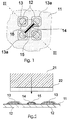
- the preferred embodiment of the invention uses a contact field consisting of four contact surfaces on the corners of an imaginary square, two of which are electrically connected to one another diagonally opposite one another. This means that adjacent contact surfaces are connected to different poles of the switch. Contact is always made when the contact bridge touches two adjacent contact surfaces. As shown in FIG. 4, a connection is already established even with incomplete key actuation, in which only the heavily drawn part of the contact bridge is active, while under the same conditions this is not the case with the known semicircular arrangement according to FIG. 3. The reliability of the contact is thus considerably improved because the number of possible contact areas has doubled.
- the contact surfaces in the diagonal shape according to the invention can be dimensioned such that, as in the known semicircular arrangement, they can be produced from an electrically conductive lacquer, preferably a carbon lacquer, because the distances are large enough to tolerate inaccuracies in a simple printing process. They are applied overlapping over copper pads, from which the connection is made by a suitable circuit board design.
- the contact surfaces are preferably square, but can also be designed as circular segments. Likewise, more than four, for example six, contact surfaces are possible.
- contact surfaces can be applied with devices that are present in any printed circuit board production, for example for component printing, high-quality keyboards can now be produced in a shorter time and with less effort.
- the contact field of a button is built up on an insulating carrier plate 11, preferably a printed circuit board.
- Copper surfaces 12 are first applied to these by a method known from printed circuit board production. These copper surfaces 12 are circular and have a diameter of approximately half the diameter of a circular contact bridge 22 arranged above them, which can be lowered by pressing a button in a known manner, which is also shown in section II-II in FIG. 2, and the maximum possible effective area 16 thereof represented as a circle is. The centers of the copper surfaces lie somewhat outside the circle that can be reached by the contact bridge.
- the copper surfaces are electrically connected to an evaluation circuit by leads, not shown.
- Contact surfaces 13 are applied to the copper surfaces 12, for example by screen printing with conductive lacquers, preferably carbon lacquer. These contact surfaces 13 overlap the copper surfaces 12 on all sides and thus additionally adhere to the carrier plate 11.
- the leads are protected in a conventional manner by a solder resist which covers the circuit board outside the contact surfaces and is likewise not shown in the figures.
- FIG. 3 the known design with semicircular surfaces is shown in FIG. 3, the maximum possible effective area 16 of the contact bridge 22 being indicated as a circle.
- the contact bridge is only partially and marginally effective, as is shown by the highlighting in FIGS. 3 to 6. This is common in input keyboards when the key heads are pressed only at the edge. 3, in the case of the arrangement according to FIG. 3 there is no connection, in the simplified diagonal arrangement with square contact surfaces in FIG. 4 a connection is achieved.
- every second contact surface is connected to one another via the center of the contact field on the surface of the contact field and the connection is designed like a contact surface.
- the connection consists of a copper track 14, which through a conductive paint track 15 - in the same way as the copper surfaces 12 - through the contact surfaces 13 is covered.
- the copper tracks are not shown in the arrangement according to FIG. 5; they are carried out in the same manner as in Fig. 1.
- the contact bridge 21 is circular with a diameter of 3.5 mm.
- the copper surfaces 12 are circular with a diameter of 1.575 mm and are centered on a square with an edge length of 2.7 mm.
- the contact surfaces 13 are square with an edge length of 2.044 mm and have rounded corners.
- Two diagonally opposite copper surfaces are connected by a 0.3 mm wide copper bar. Accordingly, the contact surfaces are connected by a web made of carbon varnish with a width of 0.6 mm. The two other contact surfaces are not rounded on the side facing this web, but bevelled so that their distance from the web is 0.512 mm.
- the distance between the contact surfaces is 0.685 mm along one side.
- the edges of the contact surfaces are at least 0.5 mm apart and the surfaces themselves are at least 0.5 mm wide, so that devices known for the application of the conductive lacquer and available for the solder mask and the component printing can be used.
- the solder stop exposure has an edge length of 4,496 mm and rounded corners.
Landscapes
- Engineering & Computer Science (AREA)
- Microelectronics & Electronic Packaging (AREA)
- Push-Button Switches (AREA)
- Manufacturing Of Printed Wiring (AREA)
- Inks, Pencil-Leads, Or Crayons (AREA)
- Printing Elements For Providing Electric Connections Between Printed Circuits (AREA)
- Wire Bonding (AREA)
- Manufacture Of Switches (AREA)
- Contacts (AREA)
Description
- Die Erfindung betrifft eine Anordnung von Kontaktflächen für Schalter, Taster und Tastaturen.
- Schalter, Taster oder Tastenfelder, insbesondere Eingabetastaturen für Datenverarbeitungsanlagen, werden häufig auf Trägerplatten aufgebaut. Dabei hat es sich als vorteilhaft erwiesen, als Trägerplatte eine Leiterplatte zu verwenden und feststehende Tastenkontakte als speziell geformte Leiterbahnen, sogenannte Kontaktflächen, auszuführen. Von dem beweglichen Teil der Taste wird eine Kontaktbrücke, häufig aus leitfähigem Gummi, beim Niederdrücken gegen die Kontaktflächen gedrückt.
- Für die Kontaktflächen wird bereits eine Anordnung von zwei benachbarten Halbkreisen wie in der DE OS 37 14 382 benutzt. Dabei werden die aus Kupfer bestehenden Kontaktflächen auf der Oberfläche vergütet, weil sonst eine mögliche Korrosion die sichere Kontaktgabe verhindern würde. Als Oberflächenvergütung wird eine galvaisch aufgetragene Goldschicht verwendet. Um die hohen Fertigungskosten der Vergoldung zu vermeiden, wird auch ein beispielsweise durch Siebdruck aufgetragener Leitlack verwendet. Für Tastaturen mit erhöhten Anforderungen an die Kontaktsicherheit ist aber die Kontaktgabe dieser Anordnung nicht ausreichend sicher. Daher wird auch eine Form wie in US 4 818 828 benutzt, bei der die Kontaktflächen fingerförmig ineinandergreifen. Die Oberflächervergütung kann jedoch bei dieser Form durch Leitlacke im Siebdruck nur bei wenigen Fingern oder großen Tastenabständen erfolgen, da der mäanderförmige Zwischenraum zwischen den Fingern so schmal sein müßte, daß die Toleranzen des Druckverfahrens für den Leitlack keine zuverlässige Herstellung erlauben.
- In dem Dokument US-A-4 029 916 wird ein Kontaktfeld gezeigt, dessen Kontaktflächen durch einen Stempel miteinander verbunden werden, symmetrisch um den Mittelpunkt des Kontaktfeldes angeordnet sind und bei dem diagonal gegenüberliegende Kontaktflächen miteinander verbunden sind. Die dargestellten Kontaktflächen sind jedoch von komplexer Form. Auch das Dokument DE-A-3 615 742 zeigt eine sehr komplexe Form der Kontaktelemente. Diese komplexen Formen der Kontaktelemente sind wie auch die fingerförmig ineinander greifenden Formen für übliche Tastenabstände nicht ohne weiteres einer Fertigung durch Leitlacke zugänglich.
- Aufgabe der Erfindung ist es, Kontaktflächen so auszuführen, daß als Oberflächenvergütung Leitlacke einsetzbar sind und eine bessere Kontaktgabe als bei der Halbkreisform erreicht wird.
- Die bevorzugte Ausführungsform der Erfindung verwendet ein Kontaktfeld aus vier Kontaktflächen auf den Ecken eines gedachten Quadrats, von denen je zwei diagonal gegenüberliegende elektisch miteinander verbunden sind. Damit sind jeweils benachbarte Kontaktflächen an verschiedene Pole des Schalters angeschlossen. Eine Kontaktgabe erfolgt also immer dann, wenn die Kontaktbrücke zwei benachbarte Kontaktflächen berührt. Wie in Fig. 4 dargestellt, wird so auch bei unvollständiger Tastenbetätigung, bei der nur der stark gezeichnete Teil der Kontaktbrücke wirksam ist, bereits ein Verbindung hergestellt, während unter den gleichen Bedingungen dies bei der bekannten Halbkreisanordnung nach Fig. 3 nicht der Fall ist. Die Zuverlässigkeit der Kontaktgabe ist damit erheblich verbessert, weil die Anzahl der möglichen Kontaktierungsflächen verdoppelt ist. Die Kontaktflächen können bei der erfindungsgemäßen Diagonalform so dimensioniert werden, daß sie, wie bei der bekannten Halbkreisanordnung, aus einem elektrisch leitfähigen Lack, vorzugsweise einem Karbonlack, hergestellt werden können, weil die Abstände groß genug sind, um Ungenauigkeiten eines einfachen Druckverfahrens zu toleriern. Sie werden überlappend über Kupfer-Pads aufgetragen, von denen aus der Anschluß durch eine geeignete Leiterplattenbahngestaltung erfolgt.
- Eine vorteilhafte Weiterbildung besteht darin, ein Paar von Kontaktflächen innerhalb des Kontaktfeldes diagonal miteinander zu verbinden. Diese Verbindung trägt zur Kontaktgabe bei; zudem ist nur noch eine um das Kontaktfeld herumführende elektrische Verbindung notwendig.
- Die Kontaktflächen werden bevorzugt quadratisch ausgestaltet, können aber auch als Kreissegmente ausgeführt werden. Gleichfalls sind mehr als vier, also beispielsweise sechs, Kontaktflächen möglich.
- Da die Kontaktflächen mit Einrichtungen aufgetragen werden können, die bei jeder Leiterplattenfertigung beispielsweise für Bestückungsdruck ohnehin vorhanden sind, können nunmehr hochwertige Tastaturen in kürzerer Zeit und mit geringerem Aufwand gefertigt werden.
- Die Erfindung wird an Hand der Zeichungen beschrieben.
- Es zeigt
- Fig. 1
- die Anordnung der Kontaktflächen in einem Kontaktfeld auf einer Leiterplatte in Draufsicht,
- Fig. 2
- einen Schnitt durch die Anordnung nach Fig.1 entlang der Linie II-II, wobei zusätzlich ein Kontaktstempel mit Kontaktbrücke dargestellt ist,
- Fig. 3
- Kontaktflächen der bekannten Anordnung in Halbkreisform mit dem Wirkungsbereich der Kontaktbrücke und markiertem Bereich für eine Teilkontaktierung,
- Fig. 4
- Kontaktflächen in Diagonal-Anordnung, ansonsten wie Fig. 3,
- Fig. 5
- vier Kreissegmente als Kontaktflächen, ansonsten wie Fig. 3,
- Nach Fig. 1 wird das Kontaktfeld einer Taste auf einem isolierenden Trägerplatte 11, vorzugsweise einer Leiterplatte, aufgebaut. Auf diese werden zunächst Kupferflächen 12 nach einem aus der Leiterplattenfertigung bekannten Verfahren aufgetragen. Diese Kupferflächen 12 sind kreisförmig und haben eine Durchmesser von etwa dem halben Durchmesser einer über ihnen angeordneten, durch Tastenbetätigung in bekannter Weise absenkbaren, kreisförmigen Kontaktbrücke 22, die auch in dem Schnitt II-II in Fig. 2 dargestellt ist und deren maximal mögliche Wirkungsfläche 16 als Kreis dargestellt ist. Die Mittelpunkte der Kupferflächen liegen etwas außerhalb des von der Kontaktbrücke erreichbaren Kreises. Die Kupferflächen werden durch nicht dargestellte Zuführungen elektrisch mit einer Auswerteschaltung verbunden. Auf die Kupferflächen 12 werden Kontaktflächen 13 aufgetragen, beispielsweise durch Siebdruck mit leitfähigen Lacken, vorzugsweise Karbonlack. Diese Kontaktflächen 13 überlappen die Kupferflächen 12 allseits und haften damit zusätzlich auf der Trägerplatte 11. Die Zuführungen werden in herkömmlicher Art durch einen Lötstoplack geschützt, der die Leiterplatte außerhalb der Kontaktflächen bedeckt und in den Abbildungen gleichfalls nicht dargestellt ist.
- Zur Verdeutlichung des Unterschieds zwischen der erfindungsgemäßen Anordnung und dem Stand der Technik ist die bekannte Ausführung mit Halbkreisflächen in Fig. 3 dargestellt, wobei die maximal mögliche Wirkungsfläche 16 der Kontaktbrücke 22 als Kreis angedeutet ist. Als Beispiel für unvollständige Betätigung sei die Kontaktbrücke nur teilweise und am Rand wirksam, wie durch die Hervorhebung in Fig. 3 bis 6 dargestellt ist. Dieser Fall ist in Eingabetastaturen häufig, wenn die Tastenköpfe nur am Rand gedrückt werden. Während in diesem Fall bei der Anordung nach Fig. 3 keine Verbindung der Kontaktflächen erfolgt, wird bei der vereinfacht dargestellten Diagonalanordnung mit quadratischen Kontaktflächen in Fig. 4 eine Verbindung erreicht.
- Gleiches gilt für die alternativen Ausführungsformen mit Kreissegmenten nach Fig. 5.
- Wie in Fig. 1 und 5 dargestellt, wird in einer Weiterbildung der Erfindung jede zweite Kontaktfläche über die Mitte des Kontaktfeldes auf der Fläche des Kontaktfeldes miteinander verbunden und die Verbindung wie eine Kontaktfläche ausgestaltet. In Fig. 1 besteht die Verbindung aus einer Kupferbahn 14, die durch eine Leitlack-Bahn 15 - in gleicher Weise wie die Kupferflächen 12 - durch die Kontaktflächen 13 überdeckt wird. In die Anordnung nach Fig. 5 sind die Kupferbahnen nicht dargestellt; sie werden in gleichartiger Weise wie in Fig. 1 ausgeführt.
- Folgende Abmessungen haben sich nach eingehender Erprobung für das Kontaktfeld einer der Norm für Schreibmaschinen entsprechenen Tastatur als besonders günstig erwiesen: Die Kontaktbrücke 21 ist kreisförmig mit einem Durchmesser von 3,5 mm. Die Kupferflächen 12 sind kreisrund mit einem Durchmesser von 1,575 mm und liegen mit ihren Mittelpunkten auf einem Quadrat mit der Kantenlänge von 2,7 mm. Die Kontaktflächen 13 sind quadratisch mit einer Kantenlänge von 2,044 mm und haben abgerundete Ecken. Zwei diagonal gegenüberliegende Kupferflächen sind durch einen Kupfersteg der Breite 0,3 mm verbunden. Entsprechend werden die Kontaktflächen durch einen Steg aus Karbonlack von 0,6 mm Breite verbunden. Die beiden anderen Kontaktflächen sind an der diesem Steg zugewandten Seite nicht abgerundet, sondern abgeschrägt, so daß ihr Abstand zum Steg 0,512 mm beträgt. Der Abstand der Kontaktflächen beträgt längs einer Seite 0,685 mm. Damit haben die Kanten der Kontaktflächen mindestens 0,5 mm Abstand und die Flächen selbst sind mindestens 0,5 mm breit, so daß für den Auftrag des Leitlacks bekannte und für die Lötstopmaske und den Bestückungsdruck vorhandene Einrichtungen verwendet werden können. Die Lötstop-Freilegung hat eine Kantenlänge von 4,496 mm und abgerundete Ecken.
Claims (7)
- Kontaktfeld für elektrische Taster und Schalter, bei dem Kontaktflächen (13, 13a) durch einen leitfähigen Kontaktstempel (22) verbunden werden, wobei- die Kontaktflächen (13, 13a) symmetrisch um den Mittelpunkt des Kontaktfelds angeordnet sind,- diagonal gegenüberliegender Paare von Kontaktflächen (13, 13a) elektrisch verbunden sind,dadurch gekennzeichnet, daß- die Kontaktflächen (13, 13a) als zwei Paare von konvexen Flächenstücken ausgebildet sind,- mindestens ein diagonal gegenüberliegendes Paar von Kontaktflächen (13) einen wesentlichen Teil der Mitte des Kontaktfeldes freiläßt.
- Kontaktfeld nach Anspruch 1, wobei die Mittelpunkte der Kontaktflächen (13, 13a) etwas außerhalb des durch den Kontaktstempel (22) erreichten Wirkungsfeldes (16) liegen.
- Kontaktfeld nach Anspruch 1 oder 2, wobei Kontaktflächen (13, 13a) im wesentlichen quadratisch sind und die lichten Abstände zwischen den Kanten der Kontaktflächen (13, 13a) zwischen der Hälfte und einem Fünftel der Seitenlänge der Kontaktflächen betragen.
- Kontaktfeld nach einem der vorhergehenden Ansprüche, wobei eines der Paare von Kontaktflächen (13a) durch die Mitte des Kontaktfeldes in der Ebene der Kontaktflächen durch einen Steg (14, 15) miteinander verbunden ist, der als zusätzliche Kontaktfläche (15) ausgebildet ist, und die zu dem Steg gerichteten Ecken der anderen beiden Kontaktflächen (13) abgeschrägt sind.
- Kontaktfeld nach einem der Ansprüche 3 oder 4 mit folgenden ungefähren Maßen für die Kontakflächen (13, 13a) und den Steg (15): Kantenlänge der Kontaktflächen 2mm, lichter Abstand 0,7mm, Entfernung der Mittelpunkte benachbarter Kontaktflächen 2,7mm, Stegbreite 0,6mm.
- Kontaktfeld nach einem der Ansprüche 1 bis 5, wobei die Kontaktflächen (13, 13a) aus elektrisch leitfähigem Lack, vorzugsweise einem Karbonlack, bestehen.
- Kontaktfeld nach Anspruch 6, wobei die Kontaktflächen (13, 13a) über vorzugsweise kreisrunden Kupferflächen (12) aufgetragen sind und diese allseits überlappen.
Applications Claiming Priority (3)
| Application Number | Priority Date | Filing Date | Title |
|---|---|---|---|
| DE4301928A DE4301928A1 (de) | 1993-01-25 | 1993-01-25 | Leitlack-Kontaktfläche |
| DE4301928 | 1993-01-25 | ||
| PCT/DE1993/001197 WO1994017541A1 (de) | 1993-01-25 | 1993-12-15 | Leitlack-kontaktfläche |
Publications (2)
| Publication Number | Publication Date |
|---|---|
| EP0680660A1 EP0680660A1 (de) | 1995-11-08 |
| EP0680660B1 true EP0680660B1 (de) | 1997-03-05 |
Family
ID=6478863
Family Applications (1)
| Application Number | Title | Priority Date | Filing Date |
|---|---|---|---|
| EP94901759A Expired - Lifetime EP0680660B1 (de) | 1993-01-25 | 1993-12-15 | Leitlack-kontaktfläche |
Country Status (6)
| Country | Link |
|---|---|
| US (1) | US5605223A (de) |
| EP (1) | EP0680660B1 (de) |
| AT (1) | ATE149738T1 (de) |
| DE (2) | DE4301928A1 (de) |
| HK (1) | HK79697A (de) |
| WO (1) | WO1994017541A1 (de) |
Families Citing this family (7)
| Publication number | Priority date | Publication date | Assignee | Title |
|---|---|---|---|---|
| DE19533427C1 (de) * | 1995-09-11 | 1996-12-05 | Kostal Leopold Gmbh & Co Kg | Elektrische Schalteinrichtung |
| US6448518B1 (en) * | 2001-06-11 | 2002-09-10 | Delphi Technologies, Inc. | Resistive switch pad |
| DE102006052462A1 (de) * | 2006-11-07 | 2008-05-08 | Amphenol-Tuchel Electronics Gmbh | Anpress-Kontakt-Array |
| DE102007003490A1 (de) * | 2007-01-24 | 2008-07-31 | Patent-Treuhand-Gesellschaft für elektrische Glühlampen mbH | Sockel für eine elektrische Lampe |
| JP2009054307A (ja) * | 2007-08-23 | 2009-03-12 | Nintendo Co Ltd | キースイッチ、入力装置、接点パターン |
| TWM404472U (en) * | 2010-12-01 | 2011-05-21 | Wistron Corp | Button mechanism and electronic device therewith |
| US8431842B2 (en) * | 2011-01-06 | 2013-04-30 | Tai-Her Yang | Sequential switching device with surrounding distinctive joint points structure |
Family Cites Families (12)
| Publication number | Priority date | Publication date | Assignee | Title |
|---|---|---|---|---|
| DE146873C (de) * | ||||
| US4029916A (en) * | 1975-04-18 | 1977-06-14 | Northern Electric Company Limited | Multi-contact push-button switch and plural embodiment for keyboard switch assembly |
| US4085306A (en) * | 1977-06-09 | 1978-04-18 | Kb-Denver, Inc. | Keyboard switch assemblies |
| DD146873A1 (de) * | 1979-11-20 | 1981-03-04 | Guenter Schieferdecker | Kontaktschicht fuer elektrische kontaktflaechen auf leiterplatten |
| US4652704A (en) * | 1985-12-30 | 1987-03-24 | Sperry Corporation | Keyboard switch |
| DE3603680A1 (de) * | 1986-02-06 | 1987-08-13 | Olympia Ag | Elektrisches schaltelement mit einer gedruckten leiterplatte |
| GB2192307B (en) * | 1986-05-02 | 1990-08-22 | Shinetsu Polymer Co | Push-button keyboard switch unit |
| DE3615742A1 (de) * | 1986-05-09 | 1987-11-12 | Schoeller & Co Elektrotech | Folientastschalter |
| US4818828A (en) * | 1988-06-17 | 1989-04-04 | Smith Corona Corporation | Electronic keyboard |
| US4987275A (en) * | 1989-07-21 | 1991-01-22 | Lucas Duralith Corporation | Multi-pole momentary membrane switch |
| DE4033129A1 (de) * | 1990-10-18 | 1992-04-23 | Hohe Electronics Gmbh & Co Ver | Schaltvorrichtung |
| US5471021A (en) * | 1994-07-18 | 1995-11-28 | Automotive Systems Laboratory, Inc. | Acceleration sensor with laterally-supported beam contacts |
-
1993
- 1993-01-25 DE DE4301928A patent/DE4301928A1/de not_active Withdrawn
- 1993-11-15 US US08/500,961 patent/US5605223A/en not_active Expired - Fee Related
- 1993-12-15 EP EP94901759A patent/EP0680660B1/de not_active Expired - Lifetime
- 1993-12-15 WO PCT/DE1993/001197 patent/WO1994017541A1/de not_active Ceased
- 1993-12-15 DE DE59305675T patent/DE59305675D1/de not_active Expired - Fee Related
- 1993-12-15 AT AT94901759T patent/ATE149738T1/de not_active IP Right Cessation
-
1997
- 1997-06-12 HK HK79697A patent/HK79697A/xx not_active IP Right Cessation
Also Published As
| Publication number | Publication date |
|---|---|
| DE59305675D1 (de) | 1997-04-10 |
| WO1994017541A1 (de) | 1994-08-04 |
| HK79697A (en) | 1997-06-20 |
| ATE149738T1 (de) | 1997-03-15 |
| DE4301928A1 (de) | 1994-07-28 |
| US5605223A (en) | 1997-02-25 |
| EP0680660A1 (de) | 1995-11-08 |
Similar Documents
| Publication | Publication Date | Title |
|---|---|---|
| DE2508154B2 (de) | Eingabeplatte | |
| DE2005565A1 (de) | ||
| DE4444923A1 (de) | Gedruckte Schaltkarte mit E/A Anschlußflächen auf Nebenflächen | |
| DE4217205A1 (de) | Steckverbinder | |
| EP0088365A1 (de) | Tastatur | |
| DE1515423A1 (de) | Kreuzschienenverteiler | |
| DE4301928A1 (de) | Leitlack-Kontaktfläche | |
| EP0131185A2 (de) | Tastenschalter | |
| DE7310839U (de) | Codierschalter | |
| DD140510A1 (de) | Vielfachtastelement | |
| DE2024563A1 (de) | Steckverbindung | |
| DE3507482C2 (de) | ||
| DE2748271C3 (de) | Gedruckte Leiterplatte und Verfahren zur Herstellung derselben | |
| EP0193173A2 (de) | Rechteckförmiger Kontaktträger für Tastaturen | |
| EP0124862A2 (de) | Tastenfeld | |
| DE19528574C2 (de) | Schaltvorrichtung | |
| DE2162438A1 (de) | Verfahren zum herstellen eines elektrodendruckkopfes | |
| DE1590625B1 (de) | Kombinierter Tasten- und Steckerstreifen | |
| DE3422094A1 (de) | Vorrichtung zum rangieren von elektrischen signalen | |
| DE2326752A1 (de) | Membranmikroschalter | |
| DE1790052B1 (de) | Kontaktvorrichtung zum abtasten von kontaktstellen | |
| DE2722430C3 (de) | Elektrischer Drehschalter | |
| DE1790052C (de) | Kontaktvorrichtung zum Abtasten von Kontaktstellen | |
| DE2204522B2 (de) | Schalttastatur | |
| DE2528448A1 (de) | Elektrischer schalter |
Legal Events
| Date | Code | Title | Description |
|---|---|---|---|
| PUAI | Public reference made under article 153(3) epc to a published international application that has entered the european phase |
Free format text: ORIGINAL CODE: 0009012 |
|
| 17P | Request for examination filed |
Effective date: 19950705 |
|
| AK | Designated contracting states |
Kind code of ref document: A1 Designated state(s): AT BE CH DE DK ES FR GB IE IT LI NL SE |
|
| 17Q | First examination report despatched |
Effective date: 19951204 |
|
| GRAG | Despatch of communication of intention to grant |
Free format text: ORIGINAL CODE: EPIDOS AGRA |
|
| GRAH | Despatch of communication of intention to grant a patent |
Free format text: ORIGINAL CODE: EPIDOS IGRA |
|
| GRAH | Despatch of communication of intention to grant a patent |
Free format text: ORIGINAL CODE: EPIDOS IGRA |
|
| GRAA | (expected) grant |
Free format text: ORIGINAL CODE: 0009210 |
|
| AK | Designated contracting states |
Kind code of ref document: B1 Designated state(s): AT BE CH DE DK ES FR GB IE IT LI NL SE |
|
| PG25 | Lapsed in a contracting state [announced via postgrant information from national office to epo] |
Ref country code: ES Free format text: THE PATENT HAS BEEN ANNULLED BY A DECISION OF A NATIONAL AUTHORITY Effective date: 19970305 Ref country code: DK Effective date: 19970305 |
|
| REF | Corresponds to: |
Ref document number: 149738 Country of ref document: AT Date of ref document: 19970315 Kind code of ref document: T |
|
| REG | Reference to a national code |
Ref country code: CH Ref legal event code: NV Representative=s name: SIEMENS SCHWEIZ AG Ref country code: CH Ref legal event code: EP |
|
| GBT | Gb: translation of ep patent filed (gb section 77(6)(a)/1977) |
Effective date: 19970318 |
|
| REF | Corresponds to: |
Ref document number: 59305675 Country of ref document: DE Date of ref document: 19970410 |
|
| ET | Fr: translation filed | ||
| REG | Reference to a national code |
Ref country code: IE Ref legal event code: FG4D Free format text: 72428 |
|
| ITF | It: translation for a ep patent filed | ||
| PG25 | Lapsed in a contracting state [announced via postgrant information from national office to epo] |
Ref country code: LI Free format text: LAPSE BECAUSE OF NON-PAYMENT OF DUE FEES Effective date: 19971231 Ref country code: CH Free format text: LAPSE BECAUSE OF NON-PAYMENT OF DUE FEES Effective date: 19971231 Ref country code: BE Free format text: LAPSE BECAUSE OF NON-PAYMENT OF DUE FEES Effective date: 19971231 |
|
| PLBE | No opposition filed within time limit |
Free format text: ORIGINAL CODE: 0009261 |
|
| STAA | Information on the status of an ep patent application or granted ep patent |
Free format text: STATUS: NO OPPOSITION FILED WITHIN TIME LIMIT |
|
| 26N | No opposition filed | ||
| BERE | Be: lapsed |
Owner name: SIEMENS NIXDORF INFORMATIONSSYSTEME A.G. Effective date: 19971231 |
|
| REG | Reference to a national code |
Ref country code: CH Ref legal event code: PL |
|
| REG | Reference to a national code |
Ref country code: FR Ref legal event code: TP |
|
| REG | Reference to a national code |
Ref country code: GB Ref legal event code: 732E |
|
| PGFP | Annual fee paid to national office [announced via postgrant information from national office to epo] |
Ref country code: SE Payment date: 20011120 Year of fee payment: 9 Ref country code: NL Payment date: 20011120 Year of fee payment: 9 Ref country code: FR Payment date: 20011120 Year of fee payment: 9 |
|
| PGFP | Annual fee paid to national office [announced via postgrant information from national office to epo] |
Ref country code: AT Payment date: 20011121 Year of fee payment: 9 |
|
| PGFP | Annual fee paid to national office [announced via postgrant information from national office to epo] |
Ref country code: GB Payment date: 20011122 Year of fee payment: 9 |
|
| PGFP | Annual fee paid to national office [announced via postgrant information from national office to epo] |
Ref country code: DE Payment date: 20011123 Year of fee payment: 9 |
|
| PGFP | Annual fee paid to national office [announced via postgrant information from national office to epo] |
Ref country code: IE Payment date: 20011217 Year of fee payment: 9 |
|
| REG | Reference to a national code |
Ref country code: GB Ref legal event code: IF02 |
|
| PG25 | Lapsed in a contracting state [announced via postgrant information from national office to epo] |
Ref country code: GB Free format text: LAPSE BECAUSE OF NON-PAYMENT OF DUE FEES Effective date: 20021215 Ref country code: AT Free format text: LAPSE BECAUSE OF NON-PAYMENT OF DUE FEES Effective date: 20021215 |
|
| PG25 | Lapsed in a contracting state [announced via postgrant information from national office to epo] |
Ref country code: SE Free format text: LAPSE BECAUSE OF NON-PAYMENT OF DUE FEES Effective date: 20021216 Ref country code: IE Free format text: LAPSE BECAUSE OF NON-PAYMENT OF DUE FEES Effective date: 20021216 |
|
| PG25 | Lapsed in a contracting state [announced via postgrant information from national office to epo] |
Ref country code: NL Free format text: LAPSE BECAUSE OF NON-PAYMENT OF DUE FEES Effective date: 20030701 Ref country code: DE Free format text: LAPSE BECAUSE OF NON-PAYMENT OF DUE FEES Effective date: 20030701 |
|
| EUG | Se: european patent has lapsed | ||
| GBPC | Gb: european patent ceased through non-payment of renewal fee |
Effective date: 20021215 |
|
| NLV4 | Nl: lapsed or anulled due to non-payment of the annual fee |
Effective date: 20030701 |
|
| PG25 | Lapsed in a contracting state [announced via postgrant information from national office to epo] |
Ref country code: FR Free format text: LAPSE BECAUSE OF NON-PAYMENT OF DUE FEES Effective date: 20030901 |
|
| REG | Reference to a national code |
Ref country code: IE Ref legal event code: MM4A |
|
| REG | Reference to a national code |
Ref country code: FR Ref legal event code: ST |
|
| PG25 | Lapsed in a contracting state [announced via postgrant information from national office to epo] |
Ref country code: IT Free format text: LAPSE BECAUSE OF NON-PAYMENT OF DUE FEES Effective date: 20051215 |