EP0681377A2 - Frequenzspringen in digitalen zellularen Netzen - Google Patents
Frequenzspringen in digitalen zellularen Netzen Download PDFInfo
- Publication number
- EP0681377A2 EP0681377A2 EP95302824A EP95302824A EP0681377A2 EP 0681377 A2 EP0681377 A2 EP 0681377A2 EP 95302824 A EP95302824 A EP 95302824A EP 95302824 A EP95302824 A EP 95302824A EP 0681377 A2 EP0681377 A2 EP 0681377A2
- Authority
- EP
- European Patent Office
- Prior art keywords
- bus
- time
- frequency
- messages
- memory
- Prior art date
- Legal status (The legal status is an assumption and is not a legal conclusion. Google has not performed a legal analysis and makes no representation as to the accuracy of the status listed.)
- Withdrawn
Links
Images


Classifications
-
- H—ELECTRICITY
- H04—ELECTRIC COMMUNICATION TECHNIQUE
- H04W—WIRELESS COMMUNICATION NETWORKS
- H04W88/00—Devices specially adapted for wireless communication networks, e.g. terminals, base stations or access point devices
- H04W88/08—Access point devices
-
- H—ELECTRICITY
- H04—ELECTRIC COMMUNICATION TECHNIQUE
- H04B—TRANSMISSION
- H04B7/00—Radio transmission systems, i.e. using radiation field
- H04B7/24—Radio transmission systems, i.e. using radiation field for communication between two or more posts
- H04B7/26—Radio transmission systems, i.e. using radiation field for communication between two or more posts at least one of which is mobile
- H04B7/2621—Radio transmission systems, i.e. using radiation field for communication between two or more posts at least one of which is mobile using frequency division multiple access [FDMA]
-
- H—ELECTRICITY
- H04—ELECTRIC COMMUNICATION TECHNIQUE
- H04J—MULTIPLEX COMMUNICATION
- H04J13/00—Code division multiplex systems
Definitions
- This application relates to Time Division Multiple Access (TDMA) systems.
- TDMA Time Division Multiple Access
- the cellular base station includes radio channel units that transmit to and receive from a plurality of users. Therefore, each unit will transmit and receive an "air" or "broadcast” frame comprising multiple time slots.
- the radio channel units are divided into a channel control unit and a plurality of transceivers which are coupled together by a transmit-receive (TRX) bus.
- TRX transmit-receive
- Each transceiver typically serves eight users, and an air frame includes eight time slots.
- the invention is a circuit for varying the carrier frequencies of transmission and reception of messages in a Time Division Multiple Access system at a baseband signal stage.
- the circuit includes means for determining the carrier frequency for transmission and reception of messages in a particular broadcast frame and for designating time slots for said messages according to frequency.
- a bus is provided for transmission and reception of messages in the designated time slots in time division multiplexed frames.
- a dual port random access memory has one port coupled to the frequency determining means and another port coupled to the bus so as to store therein said messages at locations corresponding to the designated time slots.
- a plurality of transceivers is coupled to the bus, each transceiver adapted to transmit and receive on a single carrier frequency messages assigned to specific time slots corresponding to that transceiver.
- FIG. 1 illustrates a Standard Global System for Mobile Communications (GSM) system for radio transmission as implemented by an AT&T IntelliverseTM system.
- Channel control units CCU
- TDM time division multiplex
- TRX transmit-receive
- TDM time division multiplex
- TRX transmit-receive
- each transceiver e.g., 14, will transmit radio frequency (RF) signals to and receive RF signals from a number of mobile end users, e.g., 18.
- RF radio frequency
- time division multiplexed signals are transmitted in a single broadcast frame so that eight users could be served by a single transceiver.
- the channel control unit e.g., 10, will determine what frequency to be used for each user in each frame and direct baseband signals to the appropriate transceiver adapted to the desired frequency.
- FIG. 2 illustrates a circuit in accordance with the invention which performs the frequency hopping function in the baseband portion of the base station, rather than in the RF (transceiver) portion.
- a fast microprocessor such as a digital signal processor (DSP), 21, for determining the frequency to be transmitted and received between the station and the end users in any particular broadcast frame.
- DSP digital signal processor
- This "hopping" DSP also includes a table (54) for matching the calculated frequencies with time slots in time division multiplexed frames on bus 40.
- the "hopping" DSP is coupled to one port of a dual port random access memory (DPRAM) 22.
- DPRAM dual port random access memory
- data will be transmitted between the DSP 21 and DPRAM 22 on lead 23, while the DPRAM will be addressed by the DSP on lead 24.
- a request to write will be transmitted on lead 25, and a request to read the memory will be transmitted on lead 26.
- the selection of the particular memory 22 shown is provided on lead 27.
- the other port of DPRAM 22 is coupled to a buffer circuit 28 and to a time generator and decoder circuit 29. Specifically, data is transmitted between the DPRAM 22 and buffer 28 on lead 30, while a portion of the data is transmitted to time generator and decoder circuit 29 on lead 31.
- the DPRAM is addressed by time generator and decoder circuit 29 on lead 32. Write, read and chip select requests are transmitted by the time generator and decoder circuit 29 on leads 33, 34 and 35, respectively.
- a lead 36 is also coupled between the time generator and decoder circuit 29 and the DPRAM, while a lead 37 is coupled from the time generator and decoder circuit 29, through an inverter 38, to the port of the DPRAM coupled to the hopping DSP 21.
- the time generator and decoder circuit 29 is also coupled to the buffer 28 by means of leads 39 and 39a.
- the time generator and decoder circuit 29 also includes a counter, 55, which is coupled through the time generator to a TRX clock buffer 56 and, ultimately, to clock leads 43 and 44 and to lead 42 which transmits frame signals.
- the counter is also coupled to address lead 32.
- the time generator and decoder circuit 29 is also coupled to the TRX bus through a GSM clock buffer 57, lead 58 which transmits broadcast frame signals, and lead 59 which transmits time slot signals.
- the unit 29 is further coupled to the hopping DSP 21 by leads 45-48.
- a plurality of transceivers are also coupled to the TRX bus.
- Each transceiver e.g., 50, is adapted to transmit and receive RF signals between the base station and a multiplicity of users (typically eight), e.g., 54.
- Each transceiver is tuned to a single frequency.
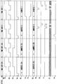
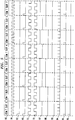
- FIGS. 3 and 4 illustrate signals relevant to the operation of the circuit 29 and DSP 21, respectively.
- a sequence of specific time division multiplexed time slots (in this example time slots 254, 255, zero and 1) is illustrated by waveform 60 of FIG. 3 and a sequence of specific time slots (also 254 to 1) is illustrated by waveform 80 of FIG. 4.
- FIGS. 3 and 4 show clock signals 61 and 62 which are received by circuit 29 from the TRX bus 40 on leads 43 and 44.
- the clock signal 62 is twice the frequency of clock signal 61, the latter typically being approximately 1.997 MHz with a period of 500.8 nanoseconds.
- each complete cycle of signal 61 defines a time slot on the TRX bus.
- Waveform 63 comprises the TRX frame signal which is transmitted to the time generator and decoder circuit 29 on lead 42 (see FIG. 4). The frame signal, when high, alerts the hardware to the coming of a new time multiplexed frame (time slot 0).
- Waveform 64 represents the "address" clock which the time generator and decoder circuit 29 generates from the incoming clock signals 61 and 62 and applies to the counter 55. It will be noted that the address clock signal 64 will go low at the start of each TRX bus time slot (defined by clock signals 61 and 62 being low). The rising edge of the signal 64 will define a new address which is equal to the time slot number address as illustrated by waveform 65 and is coupled to the dual port RAM 22 on path 32. Waveform 66 (see FIG. 4) is sent to the hopping DSP 21 on lead 45 to indicate to the DSP that a new TRX frame (time slot 0) has begun.
- the hopping DSP 21 employs a standard algorithm for calculating what frequency should be broadcast to any particular user in any particular broadcast frame.
- the DSP also includes a table, 54, allocating each possible frequency to particular TRX time slots on the TRX bus 40. Since each time slot is allocated a particular address in the DPRAM 22, the table 54 also indicates to the hopping DSP 21 which location in the memory to send a message to a particular user once the frequency has been calculated by the DSP.
- the hopping DSP will write into DPRAM the messages to the appropriate addresses according to the calculated frequencies.
- the DSP determines that user 54 is to receive a message on carrier frequency f1, it will transmit that message on lead 23 (waveform 81) to the appropriate address in DPRAM 22 by indicating that address on lead 24 (waveform 82).
- a signal will also be sent on lead 25 to indicate a write mode (waveform 70) and on lead 27 to select the particular DPRAM shown (waveform 71).
- the data written into DPRAM 22 on data lead 23 will typically comprise 9 or more bits, with 8 bits being the message and the 9th bit being an instruction bit indicating that the message is to be transmitted to the TRX bus 40. (It will be noted by the indication of "X" in waveform 81 that meaningful data will be read into the DPRAM only when the write signal (waveform 70) and chip select signal (waveform 71) are present.)
- the signals on lead 36 (waveform 73) and lead 37 (waveform 72) are always opposite in logic and will vary every time division multiplex frame (256 time slots) in order to prevent collisions between the TRX bus and the hopping DSP. That is, DSP 21 and decoder circuit 29 will always be addressing different portions of the memory at any particular time, and these portions will switch after each TRX frame.
- the time generator and decoder circuit 29 will read out the message by sending a signal on the read lead 34 (waveform 74), chip select lead 35 (waveform 75) and the appropriate address on lead 32 (waveform 65).
- the time generator determines the address from the counter 55 which counts the signals from the waveform 64 of FIG. 3 derived from the clock signals on leads 43 and 44 thereby indicating the time slot due for transmission or reception.
- the stored message will appear on lead 30 (waveform 83), and the time generator and decoder circuit 29 will examine the 9th bit of the message, which appears on lead 31, a low value indicating that the message is to be transmitted to the TRX bus 40.
- the time generator will signal the buffer 28 according to waveforms 77 and 77a after examining the 9th bit so that the buffer will be put in a transmit mode to send the message onto lead 41 and to the TRX bus 40.
- Waveform 67 indicates when valid data (the absence of "X") appears on the lead 41.
- Each transceiver, 50-53 will transmit messages only from designated time slots on the TRX bus. The message will, therefore, go to the appropriate transceiver according to the time slot initially designated by the hopper DSP. In this manner, the frequency to a particular user will vary by altering the transceiver which transmits to that user, recalling that each transceiver is fixed at a specific frequency.
- a similar operation is performed when messages are received from a user, e.g., 54, as further illustrated in FIG. 3.
- the message will be received by the appropriate transceiver, 50-53, according to the carrier frequency for that broadcast frame.
- the message will be transmitted by the TRX bus 40 to buffer 28, which has been converted to a receive mode by the communication of time generator and decoder circuit 29 on leads 39 and 39a (waveforms 77 and 77a).
- the counter 55 Based on the time slot information the counter 55 generates from clock signals on leads 43 and 44, the counter will access the address corresponding to that time slot on lead 32 (waveform 65) so that the received message will be read into the DPRAM 22 on lead 30 and stored at the address corresponding to that time slot.
- the time generator and decoder circuit 29 will apply a signal (waveform 78) on lead 33 and a signal (waveform 75) on lead 35.
- the hopping DSP 21 will then read out the stored message on lead 23 by providing the address on lead 24, a read message (waveform 79 of FIG. 4) on lead 26, and a chip select signal on lead 27 (waveform 71). The message will then be transmitted to processing circuitry (not shown) coupled to the TDM bus 20.
- the time generator and decoder circuit 29 through counter 55 also provides a page select feature in the memory by means of leads 36 and 37 and inverter 38. That is, the counter will generate 9 bits, the most significant bit appearing on lead 36 and through inverter 38 on lead 37, and the remaining 8 bits appearing on lead 32.
- the signals to one port will always be the inverse of the signal to the other port. For example, when it is desired to have the hopping DSP read or write into a block of 256 locations of the memory corresponding to the 256 time slots, a "0" will be placed on lead 37 and a "1" on lead 36 (see waveforms 72 and 73 of FIG.
- a further function performed by the time generator and decoder circuit 29 is to erase the instruction bit (9th bit) placed by the hopping DSP 21 in the DPRAM when the message was written in the memory. This is accomplished by the time generator and decoder circuit as soon as it reads out the message. During the first quarter of each time slot (e.g., 254), the decoder circuit will check to see what the 9th bit was in the previous time slot (e.g., 253). If the previous time slot indicated an output mode (a "0" for the 9th bit), the decoder circuit will write a "1" into the previous time slot address to clear the bit. If the previous time slot indicated an input mode (a "1"), nothing need be done.
- a new address will then be generated by the counter 55 (waveform 65).
- the decoder circuit will then read the 9th bit for the present time slot (e.g., 254) during the first quarter of the time slot. The remaining three quarters of the time slot can then be used for reading data into or writing data out of the memory 22. (Note, for example, that in time slot 254, data is being read out of the memory, and in the next time slot, 255, data is being read into the memory by the decoder circuit.)
- FIG. 5 illustrates the relationship between the broadcast frames of the transceivers (waveform 90) and the time division multiplexed frames of the TRX bus 40 (waveform 91). It will be noted that there are 4-1/2 TRX frames per broadcast time slot. Also shown are the signals supplied from the TRX bus 40 to the time generator and decoder circuit 29 over lead 58 (waveform 92) which indicate the start of a broadcast frame, and over lead 59 (waveform 93) to indicate the start of a broadcast time slot.
- the page select waveforms (72 and 73) are also included in FIG. 5 to illustrate how access to the memory is divided up between the time generator and decoder circuit 29 and the hopping DSP 21 during a broadcast frame.
- the start of a TRX frame is indicated to the DSP 21 by the signals on lead 45 (waveform 94).
- the DSP is also notified of the start of a broadcast time slot on lead 46 (waveform 95) and the start of a broadcast frame on lead 47 (waveform 96).
- the broadcast time slot number is transmitted to DSP 21 on lead 48 which transmits 3 bits indicated by waveforms 97-99.
Landscapes
- Engineering & Computer Science (AREA)
- Computer Networks & Wireless Communication (AREA)
- Signal Processing (AREA)
- Time-Division Multiplex Systems (AREA)
- Mobile Radio Communication Systems (AREA)
Applications Claiming Priority (2)
| Application Number | Priority Date | Filing Date | Title |
|---|---|---|---|
| US239053 | 1994-05-06 | ||
| US08/239,053 US5430713A (en) | 1994-05-06 | 1994-05-06 | Frequency hopping in digital cellular networks |
Publications (2)
| Publication Number | Publication Date |
|---|---|
| EP0681377A2 true EP0681377A2 (de) | 1995-11-08 |
| EP0681377A3 EP0681377A3 (de) | 1999-01-27 |
Family
ID=22900389
Family Applications (1)
| Application Number | Title | Priority Date | Filing Date |
|---|---|---|---|
| EP95302824A Withdrawn EP0681377A3 (de) | 1994-05-06 | 1995-04-26 | Frequenzspringen in digitalen zellularen Netzen |
Country Status (3)
| Country | Link |
|---|---|
| US (1) | US5430713A (de) |
| EP (1) | EP0681377A3 (de) |
| JP (1) | JPH07307716A (de) |
Families Citing this family (7)
| Publication number | Priority date | Publication date | Assignee | Title |
|---|---|---|---|---|
| IL114366A0 (en) * | 1995-06-27 | 1995-10-31 | Powerspectrum Technology Ltd | Apparatus and method for minimizing interference in the fringe areas of communication systems |
| FR2739740B1 (fr) * | 1995-10-06 | 1997-12-26 | Cofira Etudes Et Gestion | Procede de saut de frequence interbande dans un systeme de radiocommunication cellulaire avec des stations mobiles, et station correspondante |
| US6243565B1 (en) * | 1996-06-18 | 2001-06-05 | Telefonaktiebolaget Lm Ericsson (Publ) | Method and apparatus for transmitting communication signals using frequency and polarization diversity |
| US6006075A (en) * | 1996-06-18 | 1999-12-21 | Telefonaktiebolaget L M Ericsson (Publ) | Method and apparatus for transmitting communication signals using transmission space diversity and frequency diversity |
| WO1998042149A2 (de) * | 1997-03-19 | 1998-09-24 | Siemens Aktiengesellschaft | Verfahren und vermittlungssystem zur herstellung von fernmeldeverbindungen |
| US6230026B1 (en) * | 1998-10-15 | 2001-05-08 | Airnet Communications Corporation | Basestation architecture supporting baseband frequency hopping utilizing time division multiplexed mapping between a radio transceiver and digital signal processing resources |
| US7567620B2 (en) * | 2004-06-30 | 2009-07-28 | Texas Instruments Incorporated | Data transmission scheme using channel group and DOCSIS implementation thereof |
Family Cites Families (8)
| Publication number | Priority date | Publication date | Assignee | Title |
|---|---|---|---|---|
| US4675863A (en) * | 1985-03-20 | 1987-06-23 | International Mobile Machines Corp. | Subscriber RF telephone system for providing multiple speech and/or data signals simultaneously over either a single or a plurality of RF channels |
| IT1230400B (it) * | 1989-06-15 | 1991-10-21 | Italtel Spa | Stazione radio base per un sistema radiomobile digitale impiegante la tecnica di frequency hopping. |
| US5081641A (en) * | 1990-02-06 | 1992-01-14 | Motorola, Inc. | Interconnecting and processing system for facilitating frequency hopping |
| FI86123C (fi) * | 1990-11-15 | 1992-07-10 | Telenokia Oy | Radiosaendarmottagarsystem. |
| SE470078B (sv) * | 1992-03-27 | 1993-11-01 | Ericsson Telefon Ab L M | Basstation för cellindelade frekvenshoppande TDMA- radiokommunikationssystem |
| US5224121A (en) * | 1992-06-04 | 1993-06-29 | Motorola, Inc. | Rolling synthesizer method for baseband slow frequency hopping |
| US5263047A (en) * | 1992-07-02 | 1993-11-16 | Motorola, Inc. | Multiple cavity tuning of a transmitter output in a communication system |
| DK0590412T3 (da) * | 1992-09-28 | 1999-08-16 | Siemens Ag | Kommunikations- og styresystem inden for en biltelefonfaststation |
-
1994
- 1994-05-06 US US08/239,053 patent/US5430713A/en not_active Expired - Lifetime
-
1995
- 1995-04-26 JP JP7124510A patent/JPH07307716A/ja active Pending
- 1995-04-26 EP EP95302824A patent/EP0681377A3/de not_active Withdrawn
Also Published As
| Publication number | Publication date |
|---|---|
| EP0681377A3 (de) | 1999-01-27 |
| US5430713A (en) | 1995-07-04 |
| JPH07307716A (ja) | 1995-11-21 |
Similar Documents
| Publication | Publication Date | Title |
|---|---|---|
| US11310793B2 (en) | Techniques for setting up traffic channels in a communications system | |
| EP1366629A1 (de) | Verwaltung von burstprofileigenschaften in tdm-systemen | |
| US20030026286A1 (en) | Apparatus and method of scheduling channel allocation in dynamic TDMA frame | |
| US12342372B2 (en) | Time domain position determination method and apparatus, terminal, computer-readable medium, and chip | |
| CA2204680A1 (en) | System and method for dynamic time division access | |
| US4592049A (en) | Method of and arrangement for controlling access to a time-division multiplex message transmission path | |
| US5430713A (en) | Frequency hopping in digital cellular networks | |
| KR100448948B1 (ko) | 다이나믹 채널 할당을 이용한 공유 통신 시스템에 대한다이나믹 송신기 트레이닝 방법 | |
| HUP0004841A2 (en) | Cellular radio communications system, and subscriber station on the bases of cellular radio communications system, furtmer method of signal transmit on the bases of it | |
| US6622011B1 (en) | Paging | |
| US5710766A (en) | Method and apparatus for sharing a common bandwidth between two protocols in a radio communication system | |
| JP3388224B2 (ja) | 通信端末装置 | |
| JP3317990B2 (ja) | デジタル信号発生装置 | |
| JP3497470B2 (ja) | タイミング装置とタイミング方法 | |
| KR100346781B1 (ko) | 이동단말 및 서비스 식별자 할당방법 및 그 장치 | |
| US7016333B1 (en) | High speed timeslot assignment unit and method for a TDMA communication system | |
| JP3459644B2 (ja) | 無線通信システム端末用の同期装置 | |
| JP2000513172A (ja) | 複数の搬送周波数のtdma送信方法、ならびに対応する信号および受信機 | |
| AU624745B2 (en) | Packet/fast packet switch for voice and data | |
| KR100525387B1 (ko) | 대용량의 멀티캐스트 메시지 전송 방법 | |
| JP2816852B2 (ja) | 多元パケット通信方式 | |
| KR100487222B1 (ko) | 시분할 다중 접속 방식 이동 통신 단말기의 데이터 통신속도 표시 방법 | |
| KR0168800B1 (ko) | 도약 주파수 발생방법 및 장치 | |
| US10674507B2 (en) | Techniques for setting up traffic channels in a communications system | |
| JPS6394730A (ja) | 分割多重パケツト信号復元装置 |
Legal Events
| Date | Code | Title | Description |
|---|---|---|---|
| PUAI | Public reference made under article 153(3) epc to a published international application that has entered the european phase |
Free format text: ORIGINAL CODE: 0009012 |
|
| AK | Designated contracting states |
Kind code of ref document: A2 Designated state(s): DE FR GB IT |
|
| PUAL | Search report despatched |
Free format text: ORIGINAL CODE: 0009013 |
|
| AK | Designated contracting states |
Kind code of ref document: A3 Designated state(s): DE FR GB IT |
|
| 17P | Request for examination filed |
Effective date: 19990716 |
|
| STAA | Information on the status of an ep patent application or granted ep patent |
Free format text: STATUS: THE APPLICATION HAS BEEN WITHDRAWN |
|
| 18W | Application withdrawn |
Withdrawal date: 20020416 |