EP0682264B1 - Verfahren zur Bewertung der passiven EMV-Eigenschaften von integrierten Schaltungen und Anordnung zur Durchführung des Verfahrens - Google Patents
Verfahren zur Bewertung der passiven EMV-Eigenschaften von integrierten Schaltungen und Anordnung zur Durchführung des Verfahrens Download PDFInfo
- Publication number
- EP0682264B1 EP0682264B1 EP95106294A EP95106294A EP0682264B1 EP 0682264 B1 EP0682264 B1 EP 0682264B1 EP 95106294 A EP95106294 A EP 95106294A EP 95106294 A EP95106294 A EP 95106294A EP 0682264 B1 EP0682264 B1 EP 0682264B1
- Authority
- EP
- European Patent Office
- Prior art keywords
- interference
- procedure
- pulse
- gate
- logical
- Prior art date
- Legal status (The legal status is an assumption and is not a legal conclusion. Google has not performed a legal analysis and makes no representation as to the accuracy of the status listed.)
- Expired - Lifetime
Links
- 238000000034 method Methods 0.000 title claims description 32
- 238000005259 measurement Methods 0.000 claims abstract description 19
- 238000010168 coupling process Methods 0.000 claims description 28
- 238000005859 coupling reaction Methods 0.000 claims description 28
- 230000008878 coupling Effects 0.000 claims description 27
- 238000011156 evaluation Methods 0.000 claims description 21
- 238000004088 simulation Methods 0.000 claims description 18
- 230000006870 function Effects 0.000 claims description 12
- 238000012360 testing method Methods 0.000 claims description 10
- 230000006698 induction Effects 0.000 claims description 8
- 230000007704 transition Effects 0.000 claims description 8
- 230000007246 mechanism Effects 0.000 claims description 6
- 230000003068 static effect Effects 0.000 claims description 6
- 230000001360 synchronised effect Effects 0.000 claims description 4
- 239000004020 conductor Substances 0.000 claims description 3
- 230000000694 effects Effects 0.000 claims description 2
- 230000036039 immunity Effects 0.000 claims description 2
- 230000001939 inductive effect Effects 0.000 claims description 2
- 239000003112 inhibitor Substances 0.000 claims 2
- 230000007257 malfunction Effects 0.000 claims 2
- 230000035945 sensitivity Effects 0.000 abstract description 42
- 238000000691 measurement method Methods 0.000 abstract description 2
- 238000006880 cross-coupling reaction Methods 0.000 abstract 1
- 230000008569 process Effects 0.000 description 6
- 239000003990 capacitor Substances 0.000 description 5
- 101100204059 Caenorhabditis elegans trap-2 gene Proteins 0.000 description 4
- 239000011159 matrix material Substances 0.000 description 4
- 230000008859 change Effects 0.000 description 3
- 230000001419 dependent effect Effects 0.000 description 3
- 238000009434 installation Methods 0.000 description 2
- 238000011835 investigation Methods 0.000 description 2
- 230000000630 rising effect Effects 0.000 description 2
- 230000001960 triggered effect Effects 0.000 description 2
- 208000032368 Device malfunction Diseases 0.000 description 1
- 230000009471 action Effects 0.000 description 1
- 238000013459 approach Methods 0.000 description 1
- 230000000712 assembly Effects 0.000 description 1
- 238000000429 assembly Methods 0.000 description 1
- 230000033228 biological regulation Effects 0.000 description 1
- 230000005540 biological transmission Effects 0.000 description 1
- 238000011161 development Methods 0.000 description 1
- 230000018109 developmental process Effects 0.000 description 1
- 230000005684 electric field Effects 0.000 description 1
- 238000005516 engineering process Methods 0.000 description 1
- 230000002452 interceptive effect Effects 0.000 description 1
- 239000002184 metal Substances 0.000 description 1
- 238000012806 monitoring device Methods 0.000 description 1
- 238000012544 monitoring process Methods 0.000 description 1
- 230000003287 optical effect Effects 0.000 description 1
- 238000010972 statistical evaluation Methods 0.000 description 1
- 238000012546 transfer Methods 0.000 description 1
- 238000011144 upstream manufacturing Methods 0.000 description 1
Images


Classifications
-
- G—PHYSICS
- G01—MEASURING; TESTING
- G01R—MEASURING ELECTRIC VARIABLES; MEASURING MAGNETIC VARIABLES
- G01R31/00—Arrangements for testing electric properties; Arrangements for locating electric faults; Arrangements for electrical testing characterised by what is being tested not provided for elsewhere
- G01R31/001—Measuring interference from external sources to, or emission from, the device under test, e.g. EMC, EMI, EMP or ESD testing
- G01R31/002—Measuring interference from external sources to, or emission from, the device under test, e.g. EMC, EMI, EMP or ESD testing where the device under test is an electronic circuit
Definitions
- the invention relates to a method for evaluation the EMC properties of integrated circuits (IC) and to an arrangement for performing this method.
- the invention enables the comparison of IC EMC properties with each other, with the IC at a defined Installation location can be operated with a defined switching function.
- CMOS complementary metal-oxide-semiconductor
- HCMOS complementary metal-oxide-semiconductor
- F a field-effect transistor
- the specialist is aware that this property of the Switching speed of the IC is dependent.
- CMOS are slower than HCMOS and therefore less sensitive.
- the mechanisms that influence the IC are not known.
- DE-A-4212751 develops a procedure for simple optical Use transmission systems and still catch spikes and in phase as well as logically correct.
- a circuit with two in a row arranged RS flip-flops and a feedback of the output signal to the Negative reset input of the first RS flip-flop via an RC element becomes spikes or pulse trains stretched and thus the transmittable limit frequency increased.
- DE-A-4224858 relates to a method and an arrangement for determining the electromagnetic compatibility (EMC) using interference generators which are operated in a suitable manner and are connected to the device to be tested or the circuit to be measured.
- the circuit to be tested is subjected to the interference pulses generated continuously or in cycles by an interference generator.
- a counter shows the number of times the interference threshold has been exceeded as a numerical value, this numerical value being a direct measure of the EMC.
- the IC users i.e. Device manufacturers, compare only in rare cases the behavior of IC different Manufacturers in the application circuits of their devices. The happens by the device behavior with different IC assemblies is examined under interference.
- the device if the IC in question is fitted on a circuit board, as intended by the application. For comparison is an IC against a defined installation location exchanged the same IC type from another manufacturer. The device prepared in this way is then subjected to an EMC test subjected. The device malfunctions that occur during the test be regarding the different IC compared. The results become the most robust IC closed.
- the testing effort is very high. The results are not generally applicable since it depends on the circuit and Device properties are dependent. Furthermore, the Statistical certainty of the results difficult to grasp.
- the interference generators used (burst generators, ESD generators) have a relatively low pulse rate.
- the Glitches rarely hit critical phases of the IC function (e.g. time of information transfer at Read the program from the ROM). In such a phase is an EMC-sensitive function of the considered Circuit (IC) activated.
- the IC is usually located only briefly at certain times in critical Phases. The critical phases can be done by your own logical sequences, or by logical sequences of its Circuit environment can be brought about. Because the Sequences of the operational logic flow generated the occurrence of a critical phase can be very be rare. The probability that the glitch of the interference generator with a relatively low probability occurring critical phase and thus checking the IC is relatively small. Long testing times are required to provide an acceptable statistical To get the confidence zone.
- the object of the invention is therefore that for the evaluation and the comparison of IC EMC properties necessary, introduce general parameters and technical To create facilities with which these parameters or parameters can be determined. So that should Expert in addition to the usual IC parameters, the corresponding EMC parameters are provided.
- Influencing parameters can be used to record these four properties derive and develop measuring circuits.
- Gate sensitivity is a fundamental parameter from IC. Other EMC parameters are based on the mechanism which is the basis of the gate sensitivity.
- the gate sensitivity characterizes the change from Disturbances in logical signals.
- the disturbance variable which on Input of the gate is present instead of a logical one Signal detected and in the gate into a logical output signal changed.
- the supposed logical signal will then be erroneously processed by the following circuits.
- Higher integrated circuits are made up of individual gates built up. These can be basic sequential circuits or characteristic of computer technology act highly integrated special circuits.
- the influencing mechanism the highly integrated IC is also based on the principle of gate influence or gate sensitivity.
- the gate interference threshold is analogous to the static and dynamic switching threshold of a gate input. For low Interference pulse widths are to achieve the interference threshold analogous to the static and dynamic switching threshold higher peak values required.
- the gates are in the range of the dynamic interference threshold for short Glitches less sensitive. But oppose it particularly short interference pulses via the device interfaces and the geometric structure of the device and the printed circuit boards up to the gate entrances. Therefore lies in transition area from static to dynamic interference threshold the most sensitive area for immunity. The The position of this transition (in the course of the characteristic curve) is therefore a measure of the sensitivity of the IC to pulse-shaped Disturbances.
- the gate input a sequence of interference pulses (interference voltage) defined form.
- the glitch parameters must an area of dynamic and the transition to static Cover interference threshold.
- the interference threshold is exceeded the glitch into a logic signal converted, which at the gate output of a pulse trap is caught.
- the pulse trap stretches the signal and forwards it for evaluation.
- the test pulse must have a defined course, the can be identified by parameters. He can e.g. the shape of a steeply rising to the peak value û and falling with the time constant ⁇ from the peak value û Own exponential pulse.
- the gate sensitivity can be measured in such a way that an interference generator is connected to the corresponding input of the IC via a switching matrix and the inputs and outputs of the IC via a distributor of an input / output unit, which at the same time performs the function of the pulse trap.
- a pulse lock which can be implemented, for example, as a filter or inductance, ensures the decoupling of the interference generator from the input / output unit.
- the logical system of an IC can consist of several functional ones Units exist that are logically linked are.
- a functional unit be a gate, which with a second functional Unity, i.e. a second gate.
- the functional units can also be a complicated one Have structure and generate logical sequences, exchange and process (e.g. ALU, register sets, PROM, ports, ADU).
- ALU addressable logic unit
- a pulse-shaped interference current is generated in a generator and fed into the inputs and outputs of the IC. All or only certain inputs or outputs can be used for the interference current feed.
- the interference current flows out through the internal structures of the IC mainly through the ground and supply voltage connection (GND, V cc ).
- Inputs / outputs not affected by the disturbance variable can use logical elements with defined EMC properties completed or by an impulse lock be separated.
- Logical connections that make up the functional units can be triggered by an interference pulse e.g. via inductive coupling L, ohmic coupling R and magnetic Coupling M can be influenced.
- an interference pulse e.g. via inductive coupling L, ohmic coupling R and magnetic Coupling M can be influenced.
- Interference current becomes interference voltages through these couplings generated. These are from signal lines connected to the Lead inputs of the functional units, tapped and overlap the logical sequences (gate influences). When critical phases are hit, logical states or sequences of the functional Unit can be changed.
- the sequence required for operational purposes and the sequence which transmits the functional errors to the outside are generated by the simulation unit.
- the sequence emitted by the IC contains errors which are recognized by the monitoring device integrated in the simulation unit.
- the disturbance variable on the generator is increased until errors occur in the sequence.
- the parameters of the associated interference pulse or the generator parameters can be used as an EMC characteristic value for the structure sensitivity.
- a current pulse can also be used as the interference pulse. Parameters can be, for example, the rise time, back time and the peak value of the current pulse. The rise time and the back time can be fixed parameters, and the current peak value can be used as an EMC characteristic value.
- the structure sensitivity can for certain logical Functional units of the IC and their special modes of operation be determined. There is a specific one for each Simulation sequence required. It must be the appropriate one Areas in the IC activated and by the evaluation unit be made controllable. This can be a statistical Evaluation may be necessary because with IC with complicated structures only for small periods of time critical phases occur and therefore only rarely from Interference pulse. To increase the probability of hits is a coordination of the interference trigger possible with the sequence sequence. A regulation or Learning effect can be used. In measurement runs the critical phases are analyzed and then used in a targeted manner become. For this, the interference generator with the simulation system be synchronized. In the simplest case it can by maintaining a certain phase difference between Glitch triggering and sequence period can be realized.
- the interference pulse generates GND increases, which are tapped from an output with a reference input RE.
- the reference input has a defined gate sensitivity and a defined input resistance.
- the reference input RE converts the GND increases into logic signals when the dynamic interference threshold is exceeded. These signals are caught by a pulse trap, stretched and fed to an evaluation device. During the measuring process, the peak value of the current pulse is increased until the pulse trap picks up a signal.
- the associated parameters of the current pulse or the generator can be used as parameters and characteristic values of the coupling.
- the output can be brought into defined logic states by sequences of a simulation unit.
- over-coupling namely coupling Via the inputs arises when the interference current however, as explained above, a part flows into the IC flows out through an entrance and at a downstream one Output (RA) generates a drop in interference voltage. If at this arrangement another input (RE) is switched, this can be influenced by the voltage drop.
- RA Output
- the partial interference current At the output resistance of the reference output RA is by the partial interference current generates an interference voltage U, which also on Reference input RE is present.
- the reference input RE converts if the dynamic interference threshold is exceeded, the interference voltage into an interfering signal from the pulse trap is caught.
- the peak value of the Current pulse increased until the pulse trap Signal.
- the associated parameters of the current pulse or the generator can be used as parameters and parameters the coupling can be used.
- a logic level can be specified by the reference output become.
- the method and the measuring arrangement can be used equally Evaluation of outputs to be used that are in tristate Condition. Instead of flowing through the entrance then the interference current from that in the tri-state Exit.-
- the magnetic field is used to determine the field sensitivity the basis is the generation of a pulsed magnetic field required in the IC area.
- the determination of the magnetic field sensitivity is thereby realized that an induction coil over the chip of the IC is attached, through which a pulsed interference current flows.
- the interference current creates a pulsed magnetic field, which in the conductor loops of the chip interference voltages induced and affects the circuits of the chip.
- the Influencing is carried out analogously to the mechanisms used in the Structure sensitivity measurements were described. You will see faulty logical signals and content recognized.
- the external logical environment of the IC can be simulated with a simulation unit. If it is a sequentially operating IC, can the critical phases of the IC are influenced in a targeted manner. In Measurement runs can identify the critical phases and then be used specifically. For this, the interference generator be synchronized with the simulation system.
- the electrical field is used as a coupling variable for the determination based on the field sensitivity, the Measuring arrangement modified in such a way that the chip a metal plate attached to the IC at a defined distance is.
- the plate and the chip or a counter plate connected to a disturbance generator and with a pulse Interference voltage applied. Through electrical coupling the chip will be affected.
- the control and evaluation can be done like magnetic fields, only that a voltage is used instead of the current becomes.
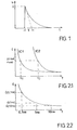
- Figures 1 to 4 serve to describe examples of implementation for measuring methods and devices for Determination of the gate sensitivity.
- the dynamic Interference / switching threshold determined.
- the position of the transition becomes dynamic Interference threshold used.
- the transition is through striking points determined. Such points represent characteristic values (Parameters) of the gate sensitivity.
- the pulse width (time constant value ⁇ ) is determined once as a parameter for a defined voltage value.
- the 20 volt value is defined as the voltage value.
- the associated value of the time constant ⁇ (20 volts) of the interference pulse is determined as described by stepwise changing of ⁇ . It can be done in such a way that at a peak value û of 20 volts the time constant is increased until the dynamic interference threshold is reached.
- the time constant value ⁇ (20 volts) can be taken from the characteristic curve of the dynamic switching threshold determined by measurement. In this way, the dynamic interference threshold for IC 1 at ⁇ 1 and IC 2 at ⁇ 2 is reached in FIG. 2.1.
- the associated voltage values û are determined as parameters for carrying out the measuring method for specific time constant values.
- the time constant values ⁇ 0.1; 1; 10 nanoseconds used.
- the peak value becomes from the measured dynamic interference threshold or the point measurements at the corresponding time constant values û (0.1ns) û (1ns) û (10ns) the associated interference voltage is determined.
- the circuit according to FIG. 3 can be used to generate the burst pulses and the influencing to be detected.
- a certain voltage level û is set.
- the capacitor C is charged to the voltage û via the resistor R v .
- contact K is closed, capacitor C is discharged via the resistor.
- a steeply rising and exponentially falling voltage pulse arises at the IC input E (gate input).
- the interference threshold of the input E is exceeded, the associated gate 1 generates a logic signal L, which is caught by the pulse trap 2 and fed to an evaluation 3.
- the time constant T can be changed by varying R and C. The course of the dynamic interference threshold or the parameters can be measured directly.
- the gate input can be a coupling and a decoupling network upstream to the investigations to be able to execute any logical level.
- FIG. 4 A measuring arrangement for IC with complicated logic Structure is shown in FIG. 4.
- the interference generator 5 is sent to the corresponding input of the IC (device under test) switched. over a distributor 6 inputs and outputs of an input / output unit 7 assigned. In this input / output unit is the function of the pulse trap is also integrated.
- a Impulse block 8 filter, choke
- the interference generator 5 be decoupled from the input / output unit 7.
- the coupling network can use elements for DC decoupling of the interference generator 5 may be included.
- a simulation unit 9 with control and Evaluation function determined via the output unit 7 logic levels or sequences are output to the IC to prepare the influence. If the output of a IC gate 1 via already free paths to an output of the IC , it is sufficient to carry out a certain IC input level to activate an output of the output unit. If not Path is free, if an unlockable path in the IC exists due to certain IC input assignments or IC input sequences a way to be unlocked. When a unlockable path does not exist, if available, IC internal logical structures for interception and Storage of the gate interference signal can be used. For this The logical structures must be in a corresponding purpose State or in an appropriate cyclical Expiry. This can be done through sequences which are delivered by the output unit. This process can via the IC inputs or outputs 10 from the simulation unit 9 are tracked.
- the simulation / control unit 9 switches an interference pulse to the desired input 10.
- generated inner logical change (gate fault signal) is when it goes directly to an output with a pulse trap 2 caught. If the logical change in the logical Structure of the IC has been saved by creating of sequences to the inputs corresponding information switched through to the outputs and the evaluation fed. Likewise, one can by influencing generated incorrect sequence sequence be monitored. The error event occurs from a certain Interference threshold, the dynamic interference threshold.
- the EMC parameters can also be selective or off a recorded characteristic can be determined. The investigation can be done in the evaluation device.
- the process can be upgraded so that e.g. just one certain type of IC via a fixed logic connection can be used.
- the switching matrix 4 and the distribution field 6 are then not required.
- uncomplicated IC can then also be used to generate logic Sequences are dispensed with.
- the measurement can also by hand without semi or fully automatic evaluation device be carried out.
- a pulse-shaped interference current i st generated by the interference generator 5 is fed via a distributor 6 into the inputs and outputs 10 or input circuits 11 and output circuits 12 of the IC.
- the interference current flows out to the outside via the internal structures and functional units 13 of the IC, in particular via the ground and supply voltage connection (GND, Vcc). Drainage can, however, also take place via the inputs / outputs not connected to the interference generator.
- These inputs / outputs can be terminated with a defined load, for example a specific gate.
- the operating and error states required for the measurement are set, detected and evaluated by the simulation unit 9 with a control and evaluation function.
- Fig. 6 shows a generator for generating the interference pulse.
- the capacitor C L is charged to the adjustable voltage û via the resistor Rv.
- the contact K discharges the capacitor C L via the resistor R and the inductance L into the IC device under test.
- the elements L and CE cause a defined rise time for the current pulse.
- the circuit also creates a constant back time. Fixed parameters for a measurement could be the rise time and the back time.
- the characteristic value of the structure influencing variable is then the peak value of the current or the charging voltage of the capacitor C L.
- the parameters of the Current pulse are measured. By comparing with the generator parameters can be adjusted to a setpoint be that the desired current flow arises.
- FIG. 7 The basic circuits for two measuring arrangements for determining the overcoupling are shown in FIG. 7; in Fig. 7.1 the coupling takes place via the outputs and in Fig. 7.2 via the inputs or via outputs in the tri-state.
- the interference current i st is supplied from the interference generator 5 via a distributor 6 and a device 14 for DC signal decoupling to the inputs and outputs 10 of the IC.
- a defined assignment of the IC inputs 10 takes place via a pulse lock 8 for decoupling the interference current pulse from the input assignment.
- the interference current i st generates ground potential (GND) increases, which are tapped from the output A with the reference input RE.
- Logic signals triggered when the dynamic interference threshold is exceeded are caught by the pulse trap 2 and sent to an evaluation 3.
- Fig. 7.2 illustrates the coupling via the inputs or outputs in the tristate state.
- the part of the circuit which is not shown and adjoins on the left is constructed analogously to FIG. 7.1.
- the interference current i st partly flows out via an input E and generates an interference voltage drop U st at the downstream output RA.
- a reference input RE connected in parallel to the reference output RA converts the interference voltage U st into an interference signal which exceeds the dynamic interference threshold and is intercepted by the pulse trap 2 and subsequently evaluated.
- the generator used for measuring the structure sensitivity can be used as the interference generator 5.
- the parameters and characteristic values used here can be used in an analogous manner.
- the arrangement according to FIG. 4 can be modified for complicated IC structures.
- FIG. 8 illustrates two measuring arrangements for determining the magnetic field sensitivity.
- An induction loop 15 is placed over the chip 16 of the IC, through which a pulsed current i st flows. Due to the magnetic field coupling, 16 interference voltages are induced in the conductor loops of the chip, which lead to evaluable faulty logic signals.
- the interference current for feeding the induction coil can be in the used for the measurement of the structure sensitivity Generator are generated.
- Parameters and parameters of the Field influence of the IC can from which the magnetic field generating interference current or from the parameters and setting values of the interference generator can be obtained.
- chip areas can be examined selectively. Areas with high sensitivity can do this be determined.
- Figure 9 shows a measuring arrangement for determining the E field sensitivity.
- An interference generator 5 is connected to the chip 16 via capacitive coupling; the other pole of the interference generator is placed on a coupling plate 17 which is at a defined distance from the chip 16.
- the interference generator can also be connected to a counter plate 18 located under the chip. The rest of the procedure is the same as for influencing the magnetic field.
Landscapes
- Physics & Mathematics (AREA)
- Electromagnetism (AREA)
- General Physics & Mathematics (AREA)
- Tests Of Electronic Circuits (AREA)
- Semiconductor Integrated Circuits (AREA)
- Testing Or Measuring Of Semiconductors Or The Like (AREA)
- Cookers (AREA)
Description
Mit den von einem Störgenerator kontinuierlich oder in Zyklen erzeugten Störimpulsen wird die zu prüfende Schaltung beaufschlagt. Die Zahl der Überschreitungen der Störschwelle pro Zeiteinheit wird von einem Zähler als Zahlenwert angezeigt, wobei dieser Zahlenwert ein direktes Maß für die EMV ist.
Eine Impulssperre, die beispielsweise als Filter oder Induktivität ausführbar ist, gewährleistet die Entkopplung des Störgenerators von der Ein-/Ausgabeeinheit.
Am Generator wird die Störgröße so weit erhöht, bis Fehler in der Sequenz auftreten. Die Parameter des zugehörigen Störimpulses oder die Generatorparameter können als EMV-Kennwert für die Strukturempfindlichkeit verwendet werden. Als Störimpuls kann auch ein Stromimpuls verwendet werden. Parameter können z.B. die Anstiegszeit, Rückenzeit und der Scheitelwert des Stromimpulses sein. Dabei können die Anstiegszeit und die Rückenzeit feste Parameter sein, und der Stromscheitelwert kann als EMV-Kennwert verwendet werden.
Durch Sequenzen einer Simulationseinheit kann der Ausgang in definierte logische Zustände gebracht werden.
Einzelheiten, Merkmale und Vorteile der Erfindung ergeben sich auch aus der nachfolgenden Beschreibung von Ausführungsbeispielen. In der zugehörigen Zeichnung zeigen
- Fig. 1
- einen Prüfimpuls mit definiertem Verlauf zur Messung der Gatterempfindlichkeit,
- Fig. 2
- zwei Meßstrategien zum Ablauf der Messung der Gatterempfindlichkeit,
- Fig. 3
- eine prinzipielle Schaltungsanordnung zur Erzeugung der Burstimpulse und zur Messung der Gatterempfindlichkeit,
- Fig. 4
- eine Meßanordnung zur Messung der Gatterempfindlichkeit für IC mit komplizierter logischer Struktur,
- Fig. 5
- eine Meßanordnung zur Bestimmung der Strukturempfindlichkeit,
- Fig. 6
- die Prinzipschaltung eines Störgenerators für die Stromimpulserzeugung,
- Fig. 7
- zwei Meßanordnungen zur Bestimmung der überkopplung,
- Fig. 8
- zwei Meßanordnungen zur Ermittlung der Feldempfindlichkeit,
- Fig. 9
- eine Meßanordnung zur Ermittlung der E-Feldempfindlichkeit.
In Fig. 2.1 ist auf diese Weise die dynamische Störschwelle für IC 1 bei τ1 und IC 2 bei τ2 erreicht.
û (0,1ns)
û (1ns)
û (10ns)
der zugehörigen Störspannung ermittelt.
Es wird eine bestimmte Spannungshöhe û eingestellt. über den Widerstand Rv wird der Kondensator C auf die Spannung û aufgeladen. Beim Schließen des Kontaktes K wird der Kondensator C über den Widerstand entladen. Am IC-Eingang E (Gattereingang) entsteht ein steil ansteigender und exponentiell abfallender Spannungsimpuls. Beim Überschreiten der Störschwelle des Eingangs E erzeugt das zugehörige Gatter 1 ein logisches Signal L, welches von der Impulsfalle 2 aufgefangen und einer Auswertug 3 zugeführt wird. Durch Variation von R und C läßt sich die Zeitkonstante T verändern. Es können der Verlauf der dynamischen Störschwelle oder die Parameter direkt gemessen werden.
Bei der Meßanordnung nach Fig. 5 zur Bestimmung der Strukturempfindlichkeit wird ein vom Störgenerator 5 erzeugter impulsförmiger Störstrom ist über einen Verteiler 6 in die Ein- und Ausgänge 10 bzw. Eingangsschaltungen 11 und Ausgangsschaltungen 12 des IC eingespeist.
Der Störstrom fließt über die inneren Strukturen und funktionellen Einheiten 13 des IC insbesondere über den Masse- und Versorgungsspannungsanschluß (GND, Vcc) nach außen ab. Ein Abfließen kann jedoch auch über die nicht mit dem Störgenerator verbundenen Ein-/Ausgänge erfolgen. Der Abschluß dieser Ein-/Ausgänge kann mit einer definierten Last, beispielsweise einem bestimmten Gatter, durchgeführt werden.
Durch die Simulationseinheit 9 mit Steuer- und Auswertefunktion werden die zur Messung erforderlichen Betriebsund Fehlerzustände eingestellt, erfaßt und ausgewertet.
Der nicht dargestellte, sich links anschließende Teil der Schaltung ist analog zu Fig. 7.1 aufgebaut.
Bei dieser Meßanordnung fließt der Störstrom ist zu einem Teil über einen Eingang E aus und erzeugt an dem nachgeordneten Ausgang RA einen Störspannungsabfall Ust. Ein parallel zum Referenzausgang RA geschalteter Referenzeingang RE wandelt bei überschreiten der dynamischen Störschwelle die Störspannung Ust in ein Störsignal, das von der Impulsfalle 2 aufgefangen und nachfolgend ausgewertet wird.
Für komplizierte IC-Strukturen kann die Anordnung nach Fig. 4 modifiziert werden.
Dabei wird über dem Chip 16 des IC eine Induktionschleife 15 plaziert, durch die ein pulsförmiger Strom ist fließt. Durch die Magnetfeldkopplung werden in den Leiterschleifen des Chips 16 Störspannungen induziert, die zu auswertbaren fehlerhaften logischen Signalen führen.
Anstelle einer kapazitiven Kopplung kann der Störgenerator auch an eine unter dem Chip befindliche Gegenplatte 18 angeschlossen werden. Im weiteren wird wie bei der Magnetfeldbeeinflussung verfahren.
Claims (14)
- Verfahren zur Bewertung der passiven EMV-Eigenschaften von integrierten Schaltungen durch ihre Beaufschlagung mit Prüfimpulsen, die von einem Störgenerator (5) erzeugt werden,
dadurch gekennzeichnet, daß die auszuwertenden EMV-IC-Parameter an den Wirkungsmechanismen der IC-Beeinflussung ansetzen und damitgemessen wird.a) über die Beeinflussung von Grundgattern die Gatterempfindlichkeit,b) über die Beeinflussung von IC-internen logischen Schaltungen die Strukturempfindlichkeit,c) über die Beeinflussung von nachgeschalteten IC die überkopplung undd) über die Beeinflussung durch IC-externe Felder die Feldempfindlichkeit - Verfahren nach Anspruch 1,
dadurch gekennzeichnet, daß die Gatterempfindlichkeit durch die Bestimmung des für die Störfestigkeit sensiblen Übergangsgebietes der statischen zur dynamischen Störschwelle, der Lage dieses übergangs im Kennlinienverlauf ermittelt wird, wozu am Gattereingang E eine Folge von Störimpulsen als Störspannung definierter Form angelegt wird, deren Parameter einen Bereich der dynamischen und den Übergang zur statischen Störschwelle abdecken und im Gatter (1) der Störimpuls bei Störschwellenüberschreitung in ein logisches Signal gewandelt wird, das am Gatterausgang (A) von einer Impulsfalle (2) aufgefangen wird, wobei durch die Impulsfalle das Signal gedehnt und zur Auswertung (3) weitergeleitet wird,
und daß der einzelne Stör- bzw. Prüfimpuls die Form eines steil auf den Scheitelwert û ansteigenden und mit der Zeitkonstante T vom Scheitelwert û abfallenden Exponentialimpulses aufweist. - Verfahren nach Anspruch 1,
dadurch gekennzeichnet, daß zur Messung der Strukturempfindlichkeit der von einem Störgenerator erzeugte impulsförmige Störstrom in die Ein- und/oder Ausgänge 10 des IC eingespeist wird, wobei alle oder nur bestimmte Ein- bzw. Ausgänge benutzbar sind und vom über die inneren Strukturen des IC hauptsächlich über den Masse- und
Versorgungsspannungsanschluß nach außen abfließenden Störstrom über induktive, ohmsche und magnetische Kopplungen Störspannungen erzeugt werden, die bei Erreichung kritischer Phasen zur Veränderung logischer Zustände oder Sequenzen der jeweiligen funktionellen Einheit (13) führen können, was von einer Simulationseinheit (9) mit Steuer- und Auswertefunktion registriert, beeinflußt und aufgezeichnet wird. - Verfahren nach Anspruch 3,
dadurch gekennzeichnet, daß nicht durch die Störgröße beaufschlagte Ein-/Ausgänge über logische Elemente mit definierten EMV-Eigenschaften abgeschlossen oder durch eine Impulssperre getrennt werden. - Verfahren nach Anspruch 3 oder 4,
dadurch gekennzeichnet, daß durch die Simulationenseinheit (9) die betriebsmäßig notwendige Sequenz und die Sequenz, die die Funktionsfehler nach außen überträgt, erzeugt wird und dabei am Generator (5) die Störgröße so weit erhöht wird, bis Fehler in der Sequenz auftreten. - Verfahren nach einem der Ansprüche 3 oder 5,
dadurch gekennzeichnet, daß die Ermittlung der Strukturempfindlichkeit für bestimmte logische Funktionseinheiten des IC und ihre speziellen Betriebsweisen durch Vorgabe einer definierten Simulations sequenz erfolgt,
und daß zur Erhöhung der Meßsicherheit eine Koordinierung der Störimpulsauslösung mit der Sequenzfolge durchgeführt werden kann, wobei ein Regelungs- bzw. Lerneffekt für die Analyse und gezielte Nutzung kritischer Phasen der Meßdurchläufe anwendbar ist und der Störgenerator (5) mit dem Simulationssystem (9) synchronisiert wird. - Verfahren nach Anspruch 1,
dadurch gekennzeichnet, daß zur Messung der überkopplung bis auf den zu überwachenden Ausgang (A) alle Ausgänge und alle Eingänge (10) oder nur spezielle Ein- und Ausgänge an den Störgenerator (5) angeschlossen werden und der Störstrom Massepotential-Anhebungen erzeugt, die mit einem Referenzeingang (RE) vom Ausgang (A) abgegriffen werden, wobei der Referenzeingang (RE) eine definierte Gatterempfindlichkeit und einen definierten Eingangswiderstand besitzt, und die Massepotential-Anhebungen vom Referenzeingang (RE) bei überschreiten der dynamischen Störschwelle in logische Signale umgewandelt werden und nachfolgend diese Signale von einer Impulsfalle (2) aufgefangen, gedehnt und einer Auswerteeinrichtung (3) zugeführt werden. - Verfahren nach Anspruch 1 und 7,
dadurch gekennzeichnet, daß der Störstrom in den IC einfließt, jedoch ein Teil über einen Eingang (E) an einem nachgeschalteten Referenzausgang (RA) einen Störspannungsabfall erzeugt und parallel zum Referenzausgang (RA) ein weiterer Eingang (RE) geschaltet wird, an dem auch die Störspannung anliegt, so daß bei überschreiten der dynamischen Störschwelle der Referenzeingang (RE) die Störspannung in eine Störsignal wandelt, das von der Impulsfalle (2) aufgenommen wird. - Verfahren nach Anspruch 8,
dadurch gekennzeichnet, daß durch den Referenzausgang (RA) ein logischer Pegel vorgegeben wird. - Verfahren nach Anspruch 7 oder 8,
dadurch gekennzeichnet, daß eine Kopplung über die Ausgänge oder über die Eingänge oder über die im Tristatezustand befindlichen Ausgänge erfolgt. - Verfahren nach Anspruch 1,
dadurch gekennzeichnet, daß zur Ermittlung der Feldempfindlichkeit auf der Grundlage von Pulsmagnetfeldern über dem Chip (16) des IC eine Induktionsspule (15) oder Induktionsschleife angeordnet wird, die mit einem pulsförmigen Störstrom beaufschlagt ist, wodurch in den
Leiterschleifen des Chips (16) Störspannungen induziert und die Schaltungen des Chips beeinflußt werden, wobei zur Ermittlung von Chipbereichen hoher Empfindlichkeit entsprechend kleine Induktionsschleifen eingesetzt werden können. - Verfahren nach Anspruch 1, 5 oder 6,
dadurch gekennzeichnet, daß die äußere logische Umgebung des IC mit einer Simulationseinheit (9) nachgebildet wird. - Anordnung zur Durchführung des Verfahrens nach Anspruch 1 oder 2,
dadurch gekennzeichnet, daß zur Messung der Gatterempfindlichkeit für IC mit komplizierter logischer Struktur ein Störgenerator (5) über ein Koppelfeld (4) an den entsprechenden Eingang (10) des IC geschaltet ist und über einen Verteiler (6) die Ein- bzw. Ausgänge (10) des IC einer Ein-/Ausgabeeinheit (7), die zugleich die Funktion der Impulsfalle (2) ausführt, zugeordnet sind, wobei durch eine Impulssperre (8), die als Filter oder Induktivität ausführbar ist, der Störgenerator (5) von der Ein-/Ausgabeeinheit (7) entkoppelt ist und die Funktionselemente Störgenerator (5), Koppelfeld (4), Verteiler (6) und Ein-/Ausgabeeinheit (7) mit einer Simulationseinheit (9) mit Steuer- und Auswertefunktion verknüpft sind. - Anordnung nach Anspruch 13,
dadurch gekennzeichnet, daß nur ein bestimmter IC-Typ über eine feste logische Verschaltung einsetzbar ist und in diesem Fall das Koppelfeld (4) und der Verteiler (6) nicht erforderlich sind.
Applications Claiming Priority (2)
| Application Number | Priority Date | Filing Date | Title |
|---|---|---|---|
| DE4417031A DE4417031C1 (de) | 1994-05-14 | 1994-05-14 | Verfahren zur Bewertung der EMV-Eigenschaften von integrierten Schaltungen und Anordnung zur Durchführung des Verfahrens |
| DE4417031 | 1994-05-14 |
Publications (3)
| Publication Number | Publication Date |
|---|---|
| EP0682264A2 EP0682264A2 (de) | 1995-11-15 |
| EP0682264A3 EP0682264A3 (de) | 1997-05-07 |
| EP0682264B1 true EP0682264B1 (de) | 1999-07-28 |
Family
ID=6518143
Family Applications (1)
| Application Number | Title | Priority Date | Filing Date |
|---|---|---|---|
| EP95106294A Expired - Lifetime EP0682264B1 (de) | 1994-05-14 | 1995-04-27 | Verfahren zur Bewertung der passiven EMV-Eigenschaften von integrierten Schaltungen und Anordnung zur Durchführung des Verfahrens |
Country Status (3)
| Country | Link |
|---|---|
| EP (1) | EP0682264B1 (de) |
| AT (1) | ATE182686T1 (de) |
| DE (2) | DE4417031C1 (de) |
Families Citing this family (3)
| Publication number | Priority date | Publication date | Assignee | Title |
|---|---|---|---|---|
| WO1999032893A1 (en) * | 1997-12-22 | 1999-07-01 | Conexant Systems, Inc. | Wireless test apparatus for integrated circuit die |
| CN109212358B (zh) * | 2018-10-17 | 2023-06-02 | 中国电力科学研究院有限公司 | 模拟变电站地电位升产生的电磁干扰的方法 |
| CN110045199B (zh) * | 2019-03-20 | 2024-05-03 | 杭州通鉴科技有限公司 | 一种eft/esd/cs电磁干扰分析仪 |
Citations (1)
| Publication number | Priority date | Publication date | Assignee | Title |
|---|---|---|---|---|
| DE4224858A1 (de) * | 1992-07-28 | 1994-02-03 | Gunter Dipl Ing Langer | Verfahren und Anordnung zur Bewertung der elektromagnetischen Verträglichkeit |
Family Cites Families (8)
| Publication number | Priority date | Publication date | Assignee | Title |
|---|---|---|---|---|
| JPS56115965A (en) * | 1980-02-19 | 1981-09-11 | Fujitsu Ltd | Testing method for semiconductor integrated circuit device |
| JPS5780577A (en) * | 1980-11-06 | 1982-05-20 | Mitsubishi Electric Corp | Testing method of semiconductor |
| EP0490116A3 (en) * | 1990-12-12 | 1992-10-14 | Vdo Adolf Schindling Ag | Method for measuring the interference potential of an integrated circuit |
| DE4041492A1 (de) * | 1990-12-22 | 1992-07-02 | Vdo Schindling | Verfahren zur messung des stoerpotentials eines ic |
| DE4110752C1 (en) * | 1991-04-03 | 1992-11-12 | Siemens Nixdorf Informationssysteme Ag, 4790 Paderborn, De | Electrostatic tester producing test pulse for electronic components - comprises charged capacitor, discharge resistors and switching elements in matrix form releasing pulse |
| DE4212751C2 (de) * | 1992-04-16 | 2001-03-01 | Langer Guenter | Verfahren und Schaltungsanordnung zur Messung der elektromagnetischen Verträglichkeit digitaler Baugruppen |
| DE4225858C2 (de) * | 1992-08-05 | 1995-05-18 | Steinmueller Gmbh L & C | Dampf-Gasturbinen-Anlage |
| DE4237828C2 (de) * | 1992-11-04 | 1996-08-01 | Eac Automation Consult Gmbh | Einrichtung zur Störungserfassung |
-
1994
- 1994-05-14 DE DE4417031A patent/DE4417031C1/de not_active Expired - Fee Related
-
1995
- 1995-04-27 AT AT95106294T patent/ATE182686T1/de not_active IP Right Cessation
- 1995-04-27 EP EP95106294A patent/EP0682264B1/de not_active Expired - Lifetime
- 1995-04-27 DE DE59506444T patent/DE59506444D1/de not_active Expired - Fee Related
Patent Citations (1)
| Publication number | Priority date | Publication date | Assignee | Title |
|---|---|---|---|---|
| DE4224858A1 (de) * | 1992-07-28 | 1994-02-03 | Gunter Dipl Ing Langer | Verfahren und Anordnung zur Bewertung der elektromagnetischen Verträglichkeit |
Also Published As
| Publication number | Publication date |
|---|---|
| DE59506444D1 (de) | 1999-09-02 |
| DE4417031C1 (de) | 1995-08-17 |
| EP0682264A3 (de) | 1997-05-07 |
| ATE182686T1 (de) | 1999-08-15 |
| EP0682264A2 (de) | 1995-11-15 |
Similar Documents
| Publication | Publication Date | Title |
|---|---|---|
| DE10191490B4 (de) | Verfahren und Vorrichtung zur Defektanalyse von integrierten Halbleiterschaltungen | |
| DE102018124351B4 (de) | Echtzeit-steigungssteuerungsvorrichtung für einen spannungsregler und verfahren zum betreiben dieser vorrichtung | |
| DE3702408C2 (de) | ||
| EP0685087B1 (de) | Selbsttestverfahren für nicht-reguläre cmos-schaltstrukturen mit hoher defekterfassung | |
| DE10053758A1 (de) | Verfahren und Vorrichtung zur Fehlersimulation bei einer integrierten Halbleiterschaltung | |
| DE10045671A1 (de) | Testvorrichtung und Testverfahren für eine integrierte Halbleiterschaltung | |
| EP2795601B1 (de) | Verfahren und vorrichtung zum erkennen einer manipulation an einer elektrischen leitung | |
| DE4441070C2 (de) | Sicherheitsschalteranordnung | |
| DE69017169T2 (de) | Testen integrierter Schaltungen unter Verwendung von Taktgeberstössen. | |
| DE69710842T2 (de) | Verfahren und Einrichtung zur Ruhestrombestimmung | |
| DE10129329A1 (de) | Fehlersimulationsverfahren und Fehlersimulator für einen Halbleiter-IC | |
| DE2418650C2 (de) | Einrichtung zur Prüfung und Überwachung von Stromversorgungseinrichtungen | |
| EP0682264B1 (de) | Verfahren zur Bewertung der passiven EMV-Eigenschaften von integrierten Schaltungen und Anordnung zur Durchführung des Verfahrens | |
| DE3686989T2 (de) | Verminderung des rauschens waehrend des pruefens von integrierten schaltungschips. | |
| DE69637490T2 (de) | Prüfbare schaltung und prüfverfahren | |
| EP0898368A2 (de) | Sensoreinrichtung | |
| DE19632457C1 (de) | Schaltungsanordnung zur Überwachung eines Sensors | |
| DE102007007339A1 (de) | Verfahren und Vorrichtung zum Lokalisieren von Fehlern auf elektronischen Leiterplatten | |
| EP0660043A1 (de) | Steuereinrichtung zur Betätigung von Schalteinrichtungen nach einem Zeitprogramm | |
| DE68924053T2 (de) | LSSD-Abfragepfad zur Berechnung der Wechselstrom-Chipsleistung. | |
| DE69419589T2 (de) | Verfahren zum prüfgerechten Entwurf von CMOS und BICMOS IC's | |
| EP0037965B1 (de) | Einrichtung zum Prüfen einer digitalen Schaltung mittels in diese Schaltung eingebauter Prüfschaltungen | |
| EP0248269A2 (de) | Verfahren zur Simulation eines Unterbrechungsfehlers in einer Logikschaltung mit Feldeffekttransistoren und Anordnungen zur Durchführung des Verfahrens | |
| DE3022279C2 (de) | ||
| EP1020733B1 (de) | Integrierte Halbleiterschaltung zur Funktionsüberprüfung von Pad-Zellen |
Legal Events
| Date | Code | Title | Description |
|---|---|---|---|
| PUAI | Public reference made under article 153(3) epc to a published international application that has entered the european phase |
Free format text: ORIGINAL CODE: 0009012 |
|
| AK | Designated contracting states |
Kind code of ref document: A2 Designated state(s): AT BE CH DE FR GB IT LI NL SE |
|
| PUAL | Search report despatched |
Free format text: ORIGINAL CODE: 0009013 |
|
| AK | Designated contracting states |
Kind code of ref document: A3 Designated state(s): AT BE CH DE FR GB IT LI NL SE |
|
| 17P | Request for examination filed |
Effective date: 19970825 |
|
| 17Q | First examination report despatched |
Effective date: 19980520 |
|
| GRAG | Despatch of communication of intention to grant |
Free format text: ORIGINAL CODE: EPIDOS AGRA |
|
| GRAG | Despatch of communication of intention to grant |
Free format text: ORIGINAL CODE: EPIDOS AGRA |
|
| GRAH | Despatch of communication of intention to grant a patent |
Free format text: ORIGINAL CODE: EPIDOS IGRA |
|
| GRAH | Despatch of communication of intention to grant a patent |
Free format text: ORIGINAL CODE: EPIDOS IGRA |
|
| GRAA | (expected) grant |
Free format text: ORIGINAL CODE: 0009210 |
|
| AK | Designated contracting states |
Kind code of ref document: B1 Designated state(s): AT BE CH DE FR GB IT LI NL SE |
|
| PG25 | Lapsed in a contracting state [announced via postgrant information from national office to epo] |
Ref country code: SE Free format text: THE PATENT HAS BEEN ANNULLED BY A DECISION OF A NATIONAL AUTHORITY Effective date: 19990728 Ref country code: NL Free format text: LAPSE BECAUSE OF FAILURE TO SUBMIT A TRANSLATION OF THE DESCRIPTION OR TO PAY THE FEE WITHIN THE PRESCRIBED TIME-LIMIT Effective date: 19990728 Ref country code: IT Free format text: LAPSE BECAUSE OF FAILURE TO SUBMIT A TRANSLATION OF THE DESCRIPTION OR TO PAY THE FEE WITHIN THE PRE;WARNING: LAPSES OF ITALIAN PATENTS WITH EFFECTIVE DATE BEFORE 2007 MAY HAVE OCCURRED AT ANY TIME BEFORE 2007. THE CORRECT EFFECTIVE DATE MAY BE DIFFERENT FROM THE ONE RECORDED.SCRIBED TIME-LIMIT Effective date: 19990728 |
|
| REF | Corresponds to: |
Ref document number: 182686 Country of ref document: AT Date of ref document: 19990815 Kind code of ref document: T |
|
| REG | Reference to a national code |
Ref country code: CH Ref legal event code: EP |
|
| REF | Corresponds to: |
Ref document number: 59506444 Country of ref document: DE Date of ref document: 19990902 |
|
| GBT | Gb: translation of ep patent filed (gb section 77(6)(a)/1977) |
Effective date: 19990910 |
|
| ET | Fr: translation filed | ||
| NLV1 | Nl: lapsed or annulled due to failure to fulfill the requirements of art. 29p and 29m of the patents act | ||
| PGFP | Annual fee paid to national office [announced via postgrant information from national office to epo] |
Ref country code: FR Payment date: 20000218 Year of fee payment: 6 |
|
| PGFP | Annual fee paid to national office [announced via postgrant information from national office to epo] |
Ref country code: GB Payment date: 20000426 Year of fee payment: 6 |
|
| PG25 | Lapsed in a contracting state [announced via postgrant information from national office to epo] |
Ref country code: AT Free format text: LAPSE BECAUSE OF NON-PAYMENT OF DUE FEES Effective date: 20000427 |
|
| PG25 | Lapsed in a contracting state [announced via postgrant information from national office to epo] |
Ref country code: LI Free format text: LAPSE BECAUSE OF NON-PAYMENT OF DUE FEES Effective date: 20000430 Ref country code: CH Free format text: LAPSE BECAUSE OF NON-PAYMENT OF DUE FEES Effective date: 20000430 Ref country code: BE Free format text: LAPSE BECAUSE OF NON-PAYMENT OF DUE FEES Effective date: 20000430 |
|
| PLBE | No opposition filed within time limit |
Free format text: ORIGINAL CODE: 0009261 |
|
| STAA | Information on the status of an ep patent application or granted ep patent |
Free format text: STATUS: NO OPPOSITION FILED WITHIN TIME LIMIT |
|
| 26N | No opposition filed | ||
| BERE | Be: lapsed |
Owner name: LANGER GUNTER Effective date: 20000430 |
|
| REG | Reference to a national code |
Ref country code: CH Ref legal event code: PL |
|
| PG25 | Lapsed in a contracting state [announced via postgrant information from national office to epo] |
Ref country code: GB Free format text: LAPSE BECAUSE OF NON-PAYMENT OF DUE FEES Effective date: 20010427 |
|
| PG25 | Lapsed in a contracting state [announced via postgrant information from national office to epo] |
Ref country code: FR Free format text: THE PATENT HAS BEEN ANNULLED BY A DECISION OF A NATIONAL AUTHORITY Effective date: 20010430 |
|
| GBPC | Gb: european patent ceased through non-payment of renewal fee |
Effective date: 20010427 |
|
| REG | Reference to a national code |
Ref country code: FR Ref legal event code: ST |
|
| PGFP | Annual fee paid to national office [announced via postgrant information from national office to epo] |
Ref country code: DE Payment date: 20030526 Year of fee payment: 9 |
|
| PG25 | Lapsed in a contracting state [announced via postgrant information from national office to epo] |
Ref country code: DE Free format text: LAPSE BECAUSE OF NON-PAYMENT OF DUE FEES Effective date: 20041103 |