EP0682464B1 - Schaltungsanordnung zum Betreiben elektrischer Lampen - Google Patents
Schaltungsanordnung zum Betreiben elektrischer Lampen Download PDFInfo
- Publication number
- EP0682464B1 EP0682464B1 EP95106673A EP95106673A EP0682464B1 EP 0682464 B1 EP0682464 B1 EP 0682464B1 EP 95106673 A EP95106673 A EP 95106673A EP 95106673 A EP95106673 A EP 95106673A EP 0682464 B1 EP0682464 B1 EP 0682464B1
- Authority
- EP
- European Patent Office
- Prior art keywords
- circuit
- voltage
- transistor
- inverter
- bridge
- Prior art date
- Legal status (The legal status is an assumption and is not a legal conclusion. Google has not performed a legal analysis and makes no representation as to the accuracy of the status listed.)
- Expired - Lifetime
Links
- 239000003990 capacitor Substances 0.000 claims description 26
- 230000001419 dependent effect Effects 0.000 claims description 10
- 230000005669 field effect Effects 0.000 claims description 5
- 230000010355 oscillation Effects 0.000 claims description 5
- 230000008878 coupling Effects 0.000 claims description 4
- 238000010168 coupling process Methods 0.000 claims description 4
- 238000005859 coupling reaction Methods 0.000 claims description 4
- 238000007599 discharging Methods 0.000 claims 3
- 238000000034 method Methods 0.000 claims 1
- 229910052736 halogen Inorganic materials 0.000 description 8
- 150000002367 halogens Chemical class 0.000 description 8
- 238000004804 winding Methods 0.000 description 8
- 238000010586 diagram Methods 0.000 description 4
- 230000001629 suppression Effects 0.000 description 2
- 230000001360 synchronised effect Effects 0.000 description 2
- 238000005516 engineering process Methods 0.000 description 1
- 238000009499 grossing Methods 0.000 description 1
- 230000010354 integration Effects 0.000 description 1
- 239000002075 main ingredient Substances 0.000 description 1
- 230000010363 phase shift Effects 0.000 description 1
- 239000004065 semiconductor Substances 0.000 description 1
Images

Classifications
-
- H—ELECTRICITY
- H05—ELECTRIC TECHNIQUES NOT OTHERWISE PROVIDED FOR
- H05B—ELECTRIC HEATING; ELECTRIC LIGHT SOURCES NOT OTHERWISE PROVIDED FOR; CIRCUIT ARRANGEMENTS FOR ELECTRIC LIGHT SOURCES, IN GENERAL
- H05B39/00—Circuit arrangements or apparatus for operating incandescent light sources
- H05B39/04—Controlling
- H05B39/041—Controlling the light-intensity of the source
- H05B39/044—Controlling the light-intensity of the source continuously
- H05B39/045—Controlling the light-intensity of the source continuously with high-frequency bridge converters
-
- H—ELECTRICITY
- H02—GENERATION; CONVERSION OR DISTRIBUTION OF ELECTRIC POWER
- H02M—APPARATUS FOR CONVERSION BETWEEN AC AND AC, BETWEEN AC AND DC, OR BETWEEN DC AND DC, AND FOR USE WITH MAINS OR SIMILAR POWER SUPPLY SYSTEMS; CONVERSION OF DC OR AC INPUT POWER INTO SURGE OUTPUT POWER; CONTROL OR REGULATION THEREOF
- H02M7/00—Conversion of AC power input into DC power output; Conversion of DC power input into AC power output
- H02M7/42—Conversion of DC power input into AC power output without possibility of reversal
- H02M7/44—Conversion of DC power input into AC power output without possibility of reversal by static converters
- H02M7/48—Conversion of DC power input into AC power output without possibility of reversal by static converters using discharge tubes with control electrode or semiconductor devices with control electrode
- H02M7/53—Conversion of DC power input into AC power output without possibility of reversal by static converters using discharge tubes with control electrode or semiconductor devices with control electrode using devices of a triode or transistor type requiring continuous application of a control signal
- H02M7/537—Conversion of DC power input into AC power output without possibility of reversal by static converters using discharge tubes with control electrode or semiconductor devices with control electrode using devices of a triode or transistor type requiring continuous application of a control signal using semiconductor devices only, e.g. single switched pulse inverters
- H02M7/5383—Conversion of DC power input into AC power output without possibility of reversal by static converters using discharge tubes with control electrode or semiconductor devices with control electrode using devices of a triode or transistor type requiring continuous application of a control signal using semiconductor devices only, e.g. single switched pulse inverters in a self-oscillating arrangement
- H02M7/53832—Conversion of DC power input into AC power output without possibility of reversal by static converters using discharge tubes with control electrode or semiconductor devices with control electrode using devices of a triode or transistor type requiring continuous application of a control signal using semiconductor devices only, e.g. single switched pulse inverters in a self-oscillating arrangement in a push-pull arrangement
-
- H—ELECTRICITY
- H05—ELECTRIC TECHNIQUES NOT OTHERWISE PROVIDED FOR
- H05B—ELECTRIC HEATING; ELECTRIC LIGHT SOURCES NOT OTHERWISE PROVIDED FOR; CIRCUIT ARRANGEMENTS FOR ELECTRIC LIGHT SOURCES, IN GENERAL
- H05B41/00—Circuit arrangements or apparatus for igniting or operating discharge lamps
- H05B41/14—Circuit arrangements
- H05B41/26—Circuit arrangements in which the lamp is fed by power derived from DC by means of a converter, e.g. by high-voltage DC
- H05B41/28—Circuit arrangements in which the lamp is fed by power derived from DC by means of a converter, e.g. by high-voltage DC using static converters
- H05B41/282—Circuit arrangements in which the lamp is fed by power derived from DC by means of a converter, e.g. by high-voltage DC using static converters with semiconductor devices
- H05B41/2825—Circuit arrangements in which the lamp is fed by power derived from DC by means of a converter, e.g. by high-voltage DC using static converters with semiconductor devices by means of a bridge converter in the final stage
-
- Y—GENERAL TAGGING OF NEW TECHNOLOGICAL DEVELOPMENTS; GENERAL TAGGING OF CROSS-SECTIONAL TECHNOLOGIES SPANNING OVER SEVERAL SECTIONS OF THE IPC; TECHNICAL SUBJECTS COVERED BY FORMER USPC CROSS-REFERENCE ART COLLECTIONS [XRACs] AND DIGESTS
- Y02—TECHNOLOGIES OR APPLICATIONS FOR MITIGATION OR ADAPTATION AGAINST CLIMATE CHANGE
- Y02B—CLIMATE CHANGE MITIGATION TECHNOLOGIES RELATED TO BUILDINGS, e.g. HOUSING, HOUSE APPLIANCES OR RELATED END-USER APPLICATIONS
- Y02B20/00—Energy efficient lighting technologies, e.g. halogen lamps or gas discharge lamps
Definitions
- the invention relates to a circuit arrangement for operating electric lamps according to the preamble of claim 1.
- This type of circuit arrangement is used in particular for operating low-voltage halogen incandescent lamps on the one hand and discharge lamps, for example Fluorescent lamps, on the other hand used.
- the main ingredient is a self-excited current feedback inverter, for example in half or full bridge circuit, which converts the low-frequency mains voltage into a high-frequency voltage chopped up.
- This is done with a coupling circuit matched to the lamp type adapted to the electrical requirements of the lamp (s) to be operated.
- the coupling circuit consists of essentially from a power transformer that applies the high frequency voltage transforms the low voltage of the halogen bulbs to be used, e.g. 6, 12 or 24 V.
- Such circuit arrangements are therefore also called electronic Called converter. Their detailed mode of operation is, for example, in the EP-PS 264 765 and DE-OS 40 11 742.
- a series inductance follows the bridge transistors, which limits the lamp current.
- Can ignite the discharge the coupling circuit also has a parallel to the electrodes of the discharge lamp switched capacitor, which resonates with the series inductance is operated.
- the operation of such electronic ballasts is for example in DE-PS 29 41 822 and DE-OS 38 05 510 explained in more detail.
- the inverter is replaced by a feedback portion of the Output current controlled. This means that after switching off the mains voltage for one re-commissioning a control pulse required to the RF vibration of the To initiate the inverter.
- Electronic converters or Ballasts a start or trigger generator that takes over this task.
- the trigger generator consists of a charging capacitor, the Charging voltage when a threshold is exceeded a voltage-dependent Switching element, for example a diac, switches through and thus the high-frequency Vibration of the inverter initiated.
- a voltage-dependent Switching element for example a diac
- the generation of a high frequency vibration disturbing Trigger signal can be prevented by the voltage-dependent switching element.
- a disadvantage of this circuit is that the reverse voltage of the discharge diode must be greater than the peak value of the maximum rectified supply voltage that occurs. Typical values are in the range between approx. 300V S and 400V S. This requires large cable gaps to avoid voltage flashovers and therefore complicates further integration of this type of circuit.
- Another disadvantage of conventional converters is that the charging behavior of the charging capacitor can be influenced undesirably by the discharge diode under certain operating conditions. In particular in combination with external dimming devices, flickering may occur in the connected lamps.
- the object of the invention is to avoid this disadvantage and a circuit arrangement to be specified with as few components as possible in low-voltage technology and therefore inexpensive to implement and optionally also in terms of circuitry integrates.
- the basic idea of the invention is the charging capacitor of the trigger generator a high-resistance controllable discharge resistor in the idle state to connect in parallel. It is controlled by the HF oscillation of the Inverter by, for example, the control connection of the discharge resistor a control signal of the inverter is supplied. As long as a voltage signal is applied, the controllable discharge resistor has a low resistance and discharges the charging capacitor. If the circuit is connected to the supply voltage, it is influenced the discharge resistor does not initially charge the capacitor, so that this Charge freely and a trigger pulse to start the inverter can trigger. The discharge resistance changes while the inverter is oscillating on the other hand periodically between high-resistance and low-resistance state.
- the charging capacitor of the trigger generator becomes essentially synchronous alternately charged or discharged for HF oscillation.
- the charging time constant of the Charging capacitor is specifically chosen so that the charging capacitor during half the period of oscillation of the inverter not up to the ignition voltage of the voltage-dependent switching element of the trigger generator can charge.
- the charging capacitor can go back up to Charge the ignition voltage, the voltage-dependent switching element of the Switch through the trigger generator and thus trigger trigger to start again of the inverter.
- control connection of the controllable discharge resistor - possibly via a series resistor to influence the control behavior - Connected to the control signal of a bridge transistor of the inverter is.
- the voltage signal of one of the two secondary windings of the control transmitter used. This voltage signal then controls the one of the two half-bridge transistors and the controllable discharge resistor essentially in sync. In this way it is reliably prevented that Control signal of the bridge transistor, an undesired trigger signal is superimposed.
- controllable discharge resistor Suitable components for the controllable discharge resistor are controllable Semiconductors, for example transistors, both bipolar and field effect (FET) Guys.
- FET field effect
- a bipolar transistor its base connection and a FET whose gate connection - possibly via a series resistor - a control signal supplied from the drive transformer of the inverter.
- the circuit arrangement according to the invention is due to the controllable discharge resistance maximum approximately the ignition voltage of the voltage-dependent switching element on - when using a diac this is typically approx. 30 V - 35 V. This opens up the possibility of completely triggering the trigger circuit as an integrated circuit execute and thus the spatial dimensions of electronic converters or to further reduce ballasts.
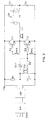
- FIG. 1 shows the basic circuit diagram of an electronic converter for low-voltage halogen incandescent lamps. It contains the function blocks radio interference suppression FE, rectifier GR, self-excited current feedback half-bridge converter - it consists of the two half-bridge transistors T1, T2, the two half-bridge capacitors C2, C3, the control transformer RKA-RKC for current feedback and the Power transformer TR - a 12 V halogen incandescent lamp is attached to its secondary winding HG operated - and a trigger generator consisting of the resistor R1, the charging capacitor C1 and the diac DC1.
- the controllable discharge resistor is realized here by an NPN transistor.
- the NPN transistor T3 and the Series resistor R2 prevent the generation of trigger pulses during the Half bridge swings.
- the radio interference suppression FE protects the network in a manner known per se from high-frequency interference signals of the half-bridge converter and is, for example, at a suppressor choke and one or more capacitors (see, for example, H.-J. Meyer, "Power Supplies for Practice", Vogel Buchverlag, Würzburg, 1989 , Pp. 115-116).
- the rectifier GR consists of a full diode bridge (see, for example, W. Hirschmann and A. Hauenstein, "Switching Power Supplies", Siemens AG, 1990, p. 102) and converts the AC voltage of the network into a pulsating DC voltage + U B.
- the negative pole of the The two bridge transistors T1, T2 are alternately switched through by the voltage signals of the two secondary windings RKB and RKC of the control transformer RKA-RKC, thus closing the circuit via the primary windings of control transformer RKA-RKC and power transformer TR, and via the two bridge capacitors C2 and C3, the secondary winding of the power transformer TR is connected to a 12 V halogen incandescent lamp, the charging capacitor C1 of the trigger generator is charged via the serial resistor R1, and the collector-emitter path of the discharge transistor T3 is connected in parallel with C1.
- the dimensioning of the discharge current of the charging capacitor C1 is deliberately limited so that sufficient initial triggering of the half-bridge converter is ensured. Otherwise, the trigger pulse could have an unsuitable shape due to a rapid discharge of the charging capacitor C1 via the discharge transistor T3.
- a trigger signal is only generated in this way when the RF oscillation of the half-bridge breaks off, for example by - possibly also only temporarily - switching off the mains voltage.
- the load circuit is not influenced by the load circuit.
- the table shows a component list for a specific exemplary embodiment.
- FIG. 2 shows a basic circuit diagram of an electronic ballast according to the invention for fluorescent lamps.
- the filter circuit FE 'corresponds in principle to Filter circuit FE described in Figure 1.
- the rectifier GR 'contains in addition a smoothing capacitor of a full diode bridge. The latter limits the degree of modulation the rectified supply voltage (modulation frequency 100 Hz) to a value that does not disturb the modulation of the luminous intensity of the fluorescent lamp LL caused.
- the inverter - it consists of a current feedback Half bridge with the two bridge capacitors T1 'and T2', the two Bridge capacitors C2 'and C3' and the control transformer RKA'-RKC '- and the trigger generator, consisting of R1 ', C1' and DC1 'correspond in their basic modes of operation that already described in Figure 1.
- the two Secondary windings RKB ', RKC' of the control transformer RKA'-RKC ' are over the Series resistors R3 and R4 with the base connections of the two bridge transistors T1 'or T2' connected.
- the controllable discharge resistance is here through the FET T3 'realized. It is a self-locking n-channel MOS-FET enrichment type.
- the inductance L1 stabilizes the Fluorescent lamp current LL. It forms a resonance circuit with the capacitance C4. Its dimensioning is chosen so that it is a during the ignition phase has high quality and its resonance frequency close to the operating frequency of the inverter. This will be used to ignite the fluorescent lamp LL necessary high ignition voltages reached.
- controllable discharge resistor can also be implemented by other components, for example p-channel MOS-FETs or the like.
- Component list for an exemplary embodiment according to the basic circuit from FIG. 1. R1 270 k ⁇ R2 1 k ⁇ C1 8.2 nF; 100 V C2, C3 15 nF; 400 V.
Landscapes
- Engineering & Computer Science (AREA)
- Power Engineering (AREA)
- Circuit Arrangements For Discharge Lamps (AREA)
Description
- Figur 1
- ein Prinzipschaltbild eines erfindungsgemäßen elektronischen Konverters für Niedervolt-Halogenglühlampen
- Figur 2
- ein Prinzipschaltbild eines erfindungsgemäßen elektronischen Vorschaltgeräts für Leuchtstofflampen.
| Bauteileliste für ein Ausführungsbeispiel gemäß der Prinzipschaltung aus Figur 1. | |
| R1 | 270 kΩ |
| R2 | 1 kΩ |
| C1 | 8,2 nF; 100 V |
| C2, C3 | 15 nF; 400 V |
| DC1 | Diac 33V |
| RKA-RKC | R 10/6/4 5/5/1 Wdgen. |
| TR | EF 25/7,5 Wdgen. |
| T1, T2 | BUL381D |
| T3 | BC850C |
| HG | Halogenglühlampe 12V, 24W |
Claims (5)
- Schaltungsanordnung zum Betreiben elektrischer Lampen bestehend ausdadurch gekennzeichnet, daß ein steuerbarer Entladewiderstand (T3, T3') parallel zum Ladekondensator (C1, C1') geschaltet ist, wobei der Steueranschluß des Entladewiderstands (T3, T3') mit einem Steuersignal des Wechselrichters verbunden ist.einer Gleichrichterschaltung (GR, GR') und optional einer Filterschaltung (FE, FE')einem selbstschwingenden stromrückgekoppelten Wechselrichter in Halboder Vollbrückenschaltungeinem Triggergenerator, der mindestens aus einer Reihenschaltung eines Ladekondensators (C1, C1') und eines Widerstandes (R1, R1') besteht, sowie ein spannungsabhängiges Schaltelement (DC1, DC1') beinhaltet, welches mit einem Verbindungspunkt zwischen Ladekondensator (C1, C1') und Widerstand (R1, R1') einerseits und dem Wechselrichter andererseits verbunden ist, wobei das spannungsabhängige Schaltelement (DC1, DC1') durchschaltet und dabei die Schwingung des Wechselrichters startet, sobald das Potential des Verbindungspunktes einen Schwellenwert überschreitet,einem Ankoppelkreis, der die hochfrequente Spannung des Wechselrichters an die zu betreibende(n) elektrische(n) Lampe(n) anpaßt
- Schaltungsanordnung nach Anspruch 1, dadurch gekennzeichnet, daß der steuerbare Entladewiderstand als Transistor (T3, T3') realisiert ist.
- Schaltungsanordnung nach Anspruch 2, dadurch gekennzeichnet, daß der Transistor als bipolarer Transistor (T3) realisiert ist, dessen Basis - eventuell über einen zusätzlichen Vorwiderstand (R2) - mit der Basisbeschaltung desjenigen Brückentransistors (T2) verbunden ist, der mit dem spannungsabhängigen Schaltelement (DC1) verschaltet ist.
- Schaltungsanordnung nach Anspruch 2, dadurch gekennzeichnet, daß der Transistor als Feldeffekttransistor (T3') realisiert ist, dessen Gate - eventuell über einen zusätzlichen Vorwiderstand - mit der Basisbeschaltung desjenigen Brückentransistors (T2') verbunden ist, der mit dem spannungsabhängigen Schaltelement (DC1') verschaltet ist.
- Schaltungsanordnung nach Anspruch 1, dadurch gekennzeichnet, daß das spannungsabhängige Schaltelement als Diac (DC1,DC1') realisiert ist.
Applications Claiming Priority (2)
| Application Number | Priority Date | Filing Date | Title |
|---|---|---|---|
| DE4416401 | 1994-05-09 | ||
| DE4416401A DE4416401A1 (de) | 1994-05-09 | 1994-05-09 | Schaltungsanordnung zum Betreiben elektrischer Lampen |
Publications (2)
| Publication Number | Publication Date |
|---|---|
| EP0682464A1 EP0682464A1 (de) | 1995-11-15 |
| EP0682464B1 true EP0682464B1 (de) | 1999-07-28 |
Family
ID=6517727
Family Applications (1)
| Application Number | Title | Priority Date | Filing Date |
|---|---|---|---|
| EP95106673A Expired - Lifetime EP0682464B1 (de) | 1994-05-09 | 1995-05-03 | Schaltungsanordnung zum Betreiben elektrischer Lampen |
Country Status (2)
| Country | Link |
|---|---|
| EP (1) | EP0682464B1 (de) |
| DE (2) | DE4416401A1 (de) |
Cited By (1)
| Publication number | Priority date | Publication date | Assignee | Title |
|---|---|---|---|---|
| DE102020130728A1 (de) | 2020-11-20 | 2022-05-25 | Osram Gmbh | Ansteuerbeschaltung für den steuereingang eines leistungstransistors eines getakteten wandlers und anwendung der ansteuerbeschaltung |
Families Citing this family (8)
| Publication number | Priority date | Publication date | Assignee | Title |
|---|---|---|---|---|
| DE19546874A1 (de) * | 1995-12-15 | 1997-06-19 | Leutz Elektronik Gmbh | Elektronisches Stromversorgungsgerät |
| DE19728295A1 (de) | 1997-07-03 | 1999-01-07 | Patent Treuhand Ges Fuer Elektrische Gluehlampen Mbh | Halbbrückenansteuerung ohne Kollektor-Vorstromspitze |
| DE19821351A1 (de) * | 1998-05-13 | 1999-11-18 | Patent Treuhand Ges Fuer Elektrische Gluehlampen Mbh | Schaltungsanordnung zum Betreiben elektrischer Lampen |
| DE10100037A1 (de) | 2001-01-03 | 2002-07-04 | Patent Treuhand Ges Fuer Elektrische Gluehlampen Mbh | Schaltungsanordnung zum Betrieb von elektrischen Lampen |
| DE102004028799A1 (de) * | 2004-06-15 | 2006-01-05 | Patent-Treuhand-Gesellschaft für elektrische Glühlampen mbH | Schaltung zum Betrieb von Lichtquellen |
| EP2260570B8 (de) * | 2008-03-17 | 2012-02-08 | Osram AG | Anordnung zur reduzierung von energieaufnahme im bereitschaftsmodus und entsprechendes verfahren |
| EP2242336A1 (de) * | 2009-04-02 | 2010-10-20 | OSRAM Gesellschaft mit beschränkter Haftung | Wandlervorrichtung zum Betreiben von Lichtquellen, sowie entsprechendes Verfahren und Computerprogrammprodukt |
| FR3019397B1 (fr) * | 2014-03-25 | 2017-07-21 | Legrand France | Circuit d'alimentation d'un circuit electronique et dispositif de commande equipe d'un tel circuit d'alimentation |
Family Cites Families (2)
| Publication number | Priority date | Publication date | Assignee | Title |
|---|---|---|---|---|
| DE4021640A1 (de) * | 1990-07-06 | 1992-01-09 | Zumtobel Ag | Helligkeitssteuer-schaltungsanordnung |
| US5111114A (en) * | 1991-06-18 | 1992-05-05 | L.P.S. Technology Co., Ltd. | Fluorescent lamp light ballast system |
-
1994
- 1994-05-09 DE DE4416401A patent/DE4416401A1/de not_active Withdrawn
-
1995
- 1995-05-03 DE DE59506445T patent/DE59506445D1/de not_active Expired - Lifetime
- 1995-05-03 EP EP95106673A patent/EP0682464B1/de not_active Expired - Lifetime
Cited By (1)
| Publication number | Priority date | Publication date | Assignee | Title |
|---|---|---|---|---|
| DE102020130728A1 (de) | 2020-11-20 | 2022-05-25 | Osram Gmbh | Ansteuerbeschaltung für den steuereingang eines leistungstransistors eines getakteten wandlers und anwendung der ansteuerbeschaltung |
Also Published As
| Publication number | Publication date |
|---|---|
| DE4416401A1 (de) | 1995-11-16 |
| EP0682464A1 (de) | 1995-11-15 |
| DE59506445D1 (de) | 1999-09-02 |
Similar Documents
| Publication | Publication Date | Title |
|---|---|---|
| EP0763276B1 (de) | Getaktete stromversorgung zum betreiben elektrischer lampen | |
| EP0264765A2 (de) | Schaltungsanordnung zum Betrieb von Niedervolt-Halogenglühlampen | |
| EP0957662B1 (de) | Schaltungsanordnung zum Betreiben elektrischer Lampen | |
| DE60006046T2 (de) | Vorschaltgerät für Starkstromgasentladungslampe | |
| EP0056642B1 (de) | Verfahren und Schaltungsanordnung zum Heizen und Zünden sowie zum Steuern oder Regeln des Lichtstroms von Niederdruckgasentladungslampen | |
| EP2089961A1 (de) | Selbstschwingender dc-dc-wandler und verfahren dazu | |
| DE19653604A1 (de) | Vorschaltung für eine Leuchtstofflampe | |
| DE2948287C2 (de) | ||
| EP0439240B1 (de) | Elektronisches Vorschaltgerät | |
| DE3829388A1 (de) | Schaltungsanordnung zum betrieb einer last | |
| DE69315761T2 (de) | Geschützter Umrichter zur Steuerung einer Entladungslampe | |
| EP0825806B1 (de) | Schaltungsanordnung zum Betreiben von elektrischen Glühlampen | |
| EP0682464B1 (de) | Schaltungsanordnung zum Betreiben elektrischer Lampen | |
| DE3711814C2 (de) | Elektronisches Vorschaltgerät zum Betrieb von Leuchtstofflampen | |
| EP1326484B1 (de) | Betriebsgerät für Gasentladungslampen | |
| EP0331157B1 (de) | Schaltnetzgerät | |
| EP0707436B1 (de) | Schaltungsanordnung zum Betreiben von Glühlampen | |
| EP0881864B1 (de) | Schaltungsanordnung zum Betreiben elektrischer Glühlampen | |
| DD267617A1 (de) | Schaltungsanordnung eines halbbrueckenwechselrichters | |
| EP0276460A1 (de) | Schaltungsanordnung zum Betrieb einer Niederdruckentladungslampe | |
| EP0682465B1 (de) | Schaltungsanordnung zum Betreiben elektrischer Glühlampen | |
| EP1608208B1 (de) | Schaltung mit Abschalteinrichtung zum Betrieb von Lichtquellen | |
| EP0707435B1 (de) | Getaktete Stromversorgung zum Betreiben von Glühlampen | |
| EP2140735B1 (de) | Schaltungsanordnung zum zünden und betreiben mindestens einer entladungslampe | |
| WO1987000719A1 (fr) | Circuit pour l'amorcage et le fonctionnement d'au moins une lampe a decharge de faible ou de haute pression avec oscillations a frequence elevee |
Legal Events
| Date | Code | Title | Description |
|---|---|---|---|
| PUAI | Public reference made under article 153(3) epc to a published international application that has entered the european phase |
Free format text: ORIGINAL CODE: 0009012 |
|
| AK | Designated contracting states |
Kind code of ref document: A1 Designated state(s): BE DE FR GB IT NL |
|
| 17P | Request for examination filed |
Effective date: 19951204 |
|
| GRAG | Despatch of communication of intention to grant |
Free format text: ORIGINAL CODE: EPIDOS AGRA |
|
| 17Q | First examination report despatched |
Effective date: 19980922 |
|
| GRAG | Despatch of communication of intention to grant |
Free format text: ORIGINAL CODE: EPIDOS AGRA |
|
| GRAH | Despatch of communication of intention to grant a patent |
Free format text: ORIGINAL CODE: EPIDOS IGRA |
|
| GRAH | Despatch of communication of intention to grant a patent |
Free format text: ORIGINAL CODE: EPIDOS IGRA |
|
| GRAA | (expected) grant |
Free format text: ORIGINAL CODE: 0009210 |
|
| AK | Designated contracting states |
Kind code of ref document: B1 Designated state(s): BE DE FR GB IT NL |
|
| REF | Corresponds to: |
Ref document number: 59506445 Country of ref document: DE Date of ref document: 19990902 |
|
| ET | Fr: translation filed | ||
| ITF | It: translation for a ep patent filed | ||
| GBT | Gb: translation of ep patent filed (gb section 77(6)(a)/1977) |
Effective date: 19990929 |
|
| PLBE | No opposition filed within time limit |
Free format text: ORIGINAL CODE: 0009261 |
|
| STAA | Information on the status of an ep patent application or granted ep patent |
Free format text: STATUS: NO OPPOSITION FILED WITHIN TIME LIMIT |
|
| 26N | No opposition filed | ||
| REG | Reference to a national code |
Ref country code: GB Ref legal event code: IF02 |
|
| REG | Reference to a national code |
Ref country code: DE Ref legal event code: R081 Ref document number: 59506445 Country of ref document: DE Owner name: OSRAM GMBH, DE Free format text: FORMER OWNER: OSRAM GESELLSCHAFT MIT BESCHRAENKTER HAFTUNG, 81543 MUENCHEN, DE Effective date: 20111130 |
|
| REG | Reference to a national code |
Ref country code: DE Ref legal event code: R081 Ref document number: 59506445 Country of ref document: DE Owner name: OSRAM GMBH, DE Free format text: FORMER OWNER: OSRAM AG, 81543 MUENCHEN, DE Effective date: 20130205 |
|
| REG | Reference to a national code |
Ref country code: DE Ref legal event code: R081 Ref document number: 59506445 Country of ref document: DE Owner name: OSRAM GMBH, DE Free format text: FORMER OWNER: OSRAM GMBH, 81543 MUENCHEN, DE Effective date: 20130822 |
|
| PGFP | Annual fee paid to national office [announced via postgrant information from national office to epo] |
Ref country code: GB Payment date: 20140521 Year of fee payment: 20 |
|
| PGFP | Annual fee paid to national office [announced via postgrant information from national office to epo] |
Ref country code: NL Payment date: 20140521 Year of fee payment: 20 Ref country code: FR Payment date: 20140527 Year of fee payment: 20 Ref country code: IT Payment date: 20140529 Year of fee payment: 20 Ref country code: DE Payment date: 20140521 Year of fee payment: 20 |
|
| PGFP | Annual fee paid to national office [announced via postgrant information from national office to epo] |
Ref country code: BE Payment date: 20140523 Year of fee payment: 20 |
|
| REG | Reference to a national code |
Ref country code: DE Ref legal event code: R071 Ref document number: 59506445 Country of ref document: DE |
|
| REG | Reference to a national code |
Ref country code: NL Ref legal event code: V4 Effective date: 20150503 |
|
| REG | Reference to a national code |
Ref country code: GB Ref legal event code: PE20 Expiry date: 20150502 |
|
| PG25 | Lapsed in a contracting state [announced via postgrant information from national office to epo] |
Ref country code: GB Free format text: LAPSE BECAUSE OF EXPIRATION OF PROTECTION Effective date: 20150502 |