EP0683512A2 - Gravure anisotropique à plasma pour dispositifs à semi-conducteur - Google Patents
Gravure anisotropique à plasma pour dispositifs à semi-conducteur Download PDFInfo
- Publication number
- EP0683512A2 EP0683512A2 EP95106830A EP95106830A EP0683512A2 EP 0683512 A2 EP0683512 A2 EP 0683512A2 EP 95106830 A EP95106830 A EP 95106830A EP 95106830 A EP95106830 A EP 95106830A EP 0683512 A2 EP0683512 A2 EP 0683512A2
- Authority
- EP
- European Patent Office
- Prior art keywords
- resist
- wafer
- layer
- oxygen plasma
- polymeric dielectric
- Prior art date
- Legal status (The legal status is an assumption and is not a legal conclusion. Google has not performed a legal analysis and makes no representation as to the accuracy of the status listed.)
- Withdrawn
Links
Images


Classifications
-
- H—ELECTRICITY
- H10—SEMICONDUCTOR DEVICES; ELECTRIC SOLID-STATE DEVICES NOT OTHERWISE PROVIDED FOR
- H10P—GENERIC PROCESSES OR APPARATUS FOR THE MANUFACTURE OR TREATMENT OF DEVICES COVERED BY CLASS H10
- H10P50/00—Etching of wafers, substrates or parts of devices
- H10P50/20—Dry etching; Plasma etching; Reactive-ion etching
- H10P50/28—Dry etching; Plasma etching; Reactive-ion etching of insulating materials
- H10P50/286—Dry etching; Plasma etching; Reactive-ion etching of insulating materials of organic materials
- H10P50/287—Dry etching; Plasma etching; Reactive-ion etching of insulating materials of organic materials by chemical means
-
- G—PHYSICS
- G03—PHOTOGRAPHY; CINEMATOGRAPHY; ANALOGOUS TECHNIQUES USING WAVES OTHER THAN OPTICAL WAVES; ELECTROGRAPHY; HOLOGRAPHY
- G03F—PHOTOMECHANICAL PRODUCTION OF TEXTURED OR PATTERNED SURFACES, e.g. FOR PRINTING, FOR PROCESSING OF SEMICONDUCTOR DEVICES; MATERIALS THEREFOR; ORIGINALS THEREFOR; APPARATUS SPECIALLY ADAPTED THEREFOR
- G03F7/00—Photomechanical, e.g. photolithographic, production of textured or patterned surfaces, e.g. printing surfaces; Materials therefor, e.g. comprising photoresists; Apparatus specially adapted therefor
- G03F7/26—Processing photosensitive materials; Apparatus therefor
- G03F7/42—Stripping or agents therefor
- G03F7/427—Stripping or agents therefor using plasma means only
-
- H—ELECTRICITY
- H10—SEMICONDUCTOR DEVICES; ELECTRIC SOLID-STATE DEVICES NOT OTHERWISE PROVIDED FOR
- H10P—GENERIC PROCESSES OR APPARATUS FOR THE MANUFACTURE OR TREATMENT OF DEVICES COVERED BY CLASS H10
- H10P76/00—Manufacture or treatment of masks on semiconductor bodies, e.g. by lithography or photolithography
- H10P76/20—Manufacture or treatment of masks on semiconductor bodies, e.g. by lithography or photolithography of masks comprising organic materials
- H10P76/204—Manufacture or treatment of masks on semiconductor bodies, e.g. by lithography or photolithography of masks comprising organic materials of organic photoresist masks
- H10P76/2041—Photolithographic processes
Definitions
- This invention relates generally to the fabrication of semiconductor devices, and more specifically to resist strip processes.
- Semiconductors are widely used in integrated circuits for electronic applications, including radios and televisions. Such integrated circuits typically use multiple transistors fabricated in single crystal silicon. Many integrated circuits now contain multiple levels of metallization for interconnections. As geometries shrink and functional density increases, it becomes imperative to reduce the RC time constant within multi-level metallization systems.
- low-dielectric insulators are either pure polymers (e.g. parylene, BCB, teflon, polyimide) or organic spin-on glass (OSOG, e.g. silsequioxane and siloxane glass).
- OSOG organic spin-on glass
- Oxygen plasma (ash) is commonly used to remove photoresist from wafer surfaces.
- the conventional ash process is performed in barrel and down-stream reactors, and is carried out at a high temperature (approximately 250°C) for a long period of time to assure that all photoresist is completely cleared.
- high temperature ash processes not only clear photoresist from the surface of the wafer, but also remove polymer contents from low-dielectric materials, resulting in problems such as shrinking, cracking, moisture absorption, via poisoning, undercutting, and general degradation of the dielectric property of low-dielectric materials. Via integration has presented a problem in the use of low-dielectric materials.
- This invention encompasses using anisotropic plasma at a low temperature to strip resist from a semiconductor wafer.
- a semiconductor wafer is placed in reactor which contains an oxygen plasma source and an optional sensor.
- the oxygen plasma source emits oxygen plasma which is drawn towards the wafer by an electric field, exposing the surface of the wafer to anisotropic oxygen plasma.
- a sensor detects when the ashing of the photoresist of the wafer is complete, and then the plasma source is turned off.
- One embodiment is a method for removing resist from a semiconductor wafer, including the steps of coating a substrate with a polymeric dielectric layer, applying an inorganic layer over the polymeric dielectric layer, applying a resist layer over the inorganic layer, patterning the resist layer, etching the inorganic layer, and ashing the resist with an anisotropic oxygen plasma.
- Another embodiment is a system for removing resist from a semiconductor wafer, comprising a reactor, a wafer having a polymeric dielectric layer positioned within the reactor, and an oxygen plasma generator located inside the reactor.
- An advantage of the invention is the ability to remove resist from wafers with low-dielectric materials, which are sensitive to the harsh effects of traditional resist removal methods.
- the decomposition of low-dielectric constant materials, which may activate the oxidation reaction, is minimized by lowering the wafer (substrate) temperature. With the present invention, very little damage occurs to the material on the sidewall of the vias.
- Table 1 below provides an overview of the elements of the embodiments and the drawings.
- Table 1 Drawing Element Preferred or Specific Examples Generic Term Other Alternate Examples or Descriptions 10
- Semiconductor wafer 12 Silicon Substrate May include other metal interconnect layers or other semiconductor elements, (e.g. transistors, diodes); Compound semiconductors (e.g. GaAs, InP, Si/Ge, SiC) may be used in place of Si.
- 14 Aluminum alloy Metal layer Titanium with an Aluminum bilayer (TiN/Al/TiN); Alloys of Al, Cu, Mo, W, Ti; Polysilicon, silicides, nitrides, carbides; AlCu alloy with Ti or TiN underlayers; Metal interconnect layer.
- Figure 1 is a prior art drawing of a conventional ash process, which has typically in the past been performed at approximately 250°C.
- Figure 1a shows a cross-section of a via 24 of semiconductor wafer 10 before a conventional ash process.
- the wafer 10 has a substrate 12 which may, for example, contain transistors, diodes, and other semiconductor elements (not shown) as are well known in the art.
- the substrate 12 may also contain other metal interconnect layers.
- Metal interconnect layer 14 has been deposited over the substrate 12 .
- Metal interconnect layer 14 may comprise, for example, aluminum or a titanium-tungsten/aluminum bilayer.
- Oxide layer 16 has been deposited over metal layer 14 and may be made of PETEOS (plasma-enhanced tetraethoxysilane).
- Polymeric dielectric layer 18 has been deposited over the oxide layer 16 and may comprise, for example, an organic polymer or organic spin-on glass (OSOG).
- the organic spin-on glass contains a mixture of organic-silicon and oxygen-silicon bondings.
- Inorganic layer 20 has been deposited over polymeric dielectric layer 18 .
- Inorganic layer 20 is an oxide, preferably SiO2 and in this example, PETEOS.
- Photoresist layer 22 has been deposited over inorganic layer 20 , which may be made of a light-sensitive polymer. Subsequent processing steps have been performed, leaving via 24 in the semiconductor wafer 10 .
- the via 24 has typically been formed through the photoresist layer 22 , inorganic layer 20 , polymeric dielectric layer 18 , and oxide layer 16 .
- the top surface of metal layer 14 usually forms the bottom of the via 24 .
- Figure 1b shows the via profile after the conventional ash process, with damage to the polymeric dielectric layer 18 along the walls of the via 24 .
- FIG. 2 A typical environment in which the present invention may be performed is shown in Figure 2 .
- Semiconductor wafer 10 containing a polymeric dielectric layer is placed in reactor 26 which contains an oxygen plasma source 28 and a sensor 30 .
- the polymeric dielectric layer contains a percentage of polymer by weight sufficient to improve the dielectric constant of SiO2.
- the polymeric dielectric layer generally contains at least 5% (and preferably between 10% and 50%) of organic polymer by weight.
- the wafer 10 is biased negatively with regard to the oxygen plasma source 28 , for example, by connecting the wafer to ground, to direct positive ions towards the wafer.
- the ashing process of the present invention is generally performed at low temperature, between approximately -40°C and 20°C, which is achieved, for example, by the use of liquid nitrogen.
- the positively-charged oxygen plasma source 28 emits oxygen plasma which is drawn towards wafer 10 by the electric field, exposing the surface of the wafer 10 to anisotropic oxygen plasma 32 .
- the sensor 30 detects when the ashing of the photoresist of the wafer 10 is complete, and then the plasma source 28 is turned off.
- the sensor 30 may be a CO or CO2 detector; when the intensity of CO or CO2 emission decreases, the system is signalled to shut off.
- the sensor 30 provides endpoint capability for the ashing system, preventing over-ashing of the wafer.
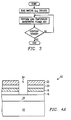
- the flow chart for the process is shown in Figure 3 .
- the wafer is biased to establish a direction for the plasma, and then the low-temperature anisotropic plasma ash is performed.
- the endpoint e.g., when the photoresist has been ashed
- the ashing ceases.
- Figure 4 The results of the new ashing process on a typical semiconductor wafer 10 is shown in Figure 4 .
- Figure 4a shows a via profile of a semiconductor before the new ash process, the same as described for Figure 1a .
- Figure 4b shows the via 24 after the ashing method of the present invention has been performed, with no damage to the polymeric dielectric layer 18 .
- Figures 1 and 4 may vary.
- Figure 5 shows an example of another semiconductor wafer 10 that could be ashed with the present invention.
- Other semiconductor structures could benefit from the low-temperature resist strip process.
- the via is typically filled with metal to form an interconnect between layers.
- Performing an ash at the low temperatures (-20° to 20) as required of this invention may result in increased time required to perform the ash, compared to conventional ashing techniques.
- the flux, or ion current may be varied to alleviate this increase in time required. For example, if the flux is increased, less time will be required to perform the ash process.
- the novel method of using a low-temperature anisotropic ash with endpoints to strip resist can offer definite advantages over the conventional processes.
- the anisotropic ions can bombard the planar surface containing the resist to be ashed, and simultaneously clean any residue off the surface of the metal. Because the ash is anisotropic, very little damage will occur to the polymeric dielectric material on the sidewall.
- the directionality of the moving oxygen species (O+) limits the reactivity of the sidewall with the oxygen.
- the endpoint capability can stop the ashing process before any damage occurs in undesirable locations, in this case to the polymeric dielectric layer sidewall of the via.
- the use of a sensor to attain the endpoint capability is optional and gives the benefit of more control to the ash process.
- the low temperature can reduce the reactivity between the polymer and the sidewall of the dielectric layer with the oxygen plasma.
- the low temperature slows the activity of the molecules, allowing a more controlled ash process.
- This invention is beneficial to other materials, particularly material sensitive to conventional ash processes.
- the invention is particularly useful for the ashing of semiconductor wafers using polymeric dielectric materials, because the damage caused to the polymeric dielectric materials by traditional methods of removing resist is undesirable and extensive, causing many problems in semiconductor manufacturing.
- the present invention a low temperature resist strip process, eliminates or minimizes such damage to the polymeric dielectric material.
- the ash process of the present invention may remove native oxide on the metal layer.
Landscapes
- Physics & Mathematics (AREA)
- Engineering & Computer Science (AREA)
- Plasma & Fusion (AREA)
- General Physics & Mathematics (AREA)
- Drying Of Semiconductors (AREA)
- Internal Circuitry In Semiconductor Integrated Circuit Devices (AREA)
- Exposure Of Semiconductors, Excluding Electron Or Ion Beam Exposure (AREA)
Applications Claiming Priority (2)
| Application Number | Priority Date | Filing Date | Title |
|---|---|---|---|
| US242922 | 1994-05-16 | ||
| US08/242,922 US5453157A (en) | 1994-05-16 | 1994-05-16 | Low temperature anisotropic ashing of resist for semiconductor fabrication |
Publications (2)
| Publication Number | Publication Date |
|---|---|
| EP0683512A2 true EP0683512A2 (fr) | 1995-11-22 |
| EP0683512A3 EP0683512A3 (fr) | 1997-11-19 |
Family
ID=22916655
Family Applications (1)
| Application Number | Title | Priority Date | Filing Date |
|---|---|---|---|
| EP95106830A Withdrawn EP0683512A3 (fr) | 1994-05-16 | 1995-05-05 | Gravure anisotropique à plasma pour dispositifs à semi-conducteur |
Country Status (5)
| Country | Link |
|---|---|
| US (1) | US5453157A (fr) |
| EP (1) | EP0683512A3 (fr) |
| JP (1) | JPH0845914A (fr) |
| KR (1) | KR950034478A (fr) |
| TW (1) | TW294834B (fr) |
Cited By (1)
| Publication number | Priority date | Publication date | Assignee | Title |
|---|---|---|---|---|
| US6165375A (en) * | 1997-09-23 | 2000-12-26 | Cypress Semiconductor Corporation | Plasma etching method |
Families Citing this family (67)
| Publication number | Priority date | Publication date | Assignee | Title |
|---|---|---|---|---|
| FR2751468A1 (fr) * | 1996-07-15 | 1998-01-23 | Lgelectronics | Procede d'attaque pour un dispositif presentant un materiau organique |
| TW425619B (en) * | 1999-06-14 | 2001-03-11 | Mosel Vitelic Inc | Process for removing photoresist by a photoresist remover using the adjustment of photoresist removing stop and the continuous sequenced arrangement of chips |
| US6346489B1 (en) | 1999-09-02 | 2002-02-12 | Applied Materials, Inc. | Precleaning process for metal plug that minimizes damage to low-κ dielectric |
| US6873087B1 (en) * | 1999-10-29 | 2005-03-29 | Board Of Regents, The University Of Texas System | High precision orientation alignment and gap control stages for imprint lithography processes |
| US6451158B1 (en) * | 1999-12-21 | 2002-09-17 | Lam Research Corporation | Apparatus for detecting the endpoint of a photoresist stripping process |
| US6323121B1 (en) | 2000-05-12 | 2001-11-27 | Taiwan Semiconductor Manufacturing Company | Fully dry post-via-etch cleaning method for a damascene process |
| SG142150A1 (en) * | 2000-07-16 | 2008-05-28 | Univ Texas | High-resolution overlay alignment systems for imprint lithography |
| KR100827741B1 (ko) | 2000-07-17 | 2008-05-07 | 보드 오브 리전츠, 더 유니버시티 오브 텍사스 시스템 | 임프린트 리소그래피 공정을 위한 자동 유체 분배 방법 및시스템 |
| JP2004505273A (ja) | 2000-08-01 | 2004-02-19 | ボード・オブ・リージエンツ,ザ・ユニバーシテイ・オブ・テキサス・システム | 転写リソグラフィのための透明テンプレートと基板の間のギャップおよび配向を高精度でセンシングするための方法 |
| AU2001286573A1 (en) | 2000-08-21 | 2002-03-04 | Board Of Regents, The University Of Texas System | Flexure based macro motion translation stage |
| CN100365507C (zh) * | 2000-10-12 | 2008-01-30 | 德克萨斯州大学系统董事会 | 用于室温下低压微刻痕和毫微刻痕光刻的模板 |
| JP3770790B2 (ja) * | 2000-11-15 | 2006-04-26 | シャープ株式会社 | アッシング方法 |
| US6964793B2 (en) | 2002-05-16 | 2005-11-15 | Board Of Regents, The University Of Texas System | Method for fabricating nanoscale patterns in light curable compositions using an electric field |
| JP2003092287A (ja) * | 2001-09-19 | 2003-03-28 | Nec Corp | アッシング方法 |
| US7037639B2 (en) | 2002-05-01 | 2006-05-02 | Molecular Imprints, Inc. | Methods of manufacturing a lithography template |
| US6926929B2 (en) | 2002-07-09 | 2005-08-09 | Molecular Imprints, Inc. | System and method for dispensing liquids |
| US7077992B2 (en) | 2002-07-11 | 2006-07-18 | Molecular Imprints, Inc. | Step and repeat imprint lithography processes |
| US6900881B2 (en) | 2002-07-11 | 2005-05-31 | Molecular Imprints, Inc. | Step and repeat imprint lithography systems |
| US6908861B2 (en) * | 2002-07-11 | 2005-06-21 | Molecular Imprints, Inc. | Method for imprint lithography using an electric field |
| US7019819B2 (en) | 2002-11-13 | 2006-03-28 | Molecular Imprints, Inc. | Chucking system for modulating shapes of substrates |
| US6932934B2 (en) | 2002-07-11 | 2005-08-23 | Molecular Imprints, Inc. | Formation of discontinuous films during an imprint lithography process |
| US7070405B2 (en) | 2002-08-01 | 2006-07-04 | Molecular Imprints, Inc. | Alignment systems for imprint lithography |
| US7027156B2 (en) | 2002-08-01 | 2006-04-11 | Molecular Imprints, Inc. | Scatterometry alignment for imprint lithography |
| US6916584B2 (en) | 2002-08-01 | 2005-07-12 | Molecular Imprints, Inc. | Alignment methods for imprint lithography |
| US7071088B2 (en) | 2002-08-23 | 2006-07-04 | Molecular Imprints, Inc. | Method for fabricating bulbous-shaped vias |
| US8349241B2 (en) | 2002-10-04 | 2013-01-08 | Molecular Imprints, Inc. | Method to arrange features on a substrate to replicate features having minimal dimensional variability |
| US6980282B2 (en) * | 2002-12-11 | 2005-12-27 | Molecular Imprints, Inc. | Method for modulating shapes of substrates |
| US6929762B2 (en) | 2002-11-13 | 2005-08-16 | Molecular Imprints, Inc. | Method of reducing pattern distortions during imprint lithography processes |
| US6871558B2 (en) * | 2002-12-12 | 2005-03-29 | Molecular Imprints, Inc. | Method for determining characteristics of substrate employing fluid geometries |
| US7452574B2 (en) | 2003-02-27 | 2008-11-18 | Molecular Imprints, Inc. | Method to reduce adhesion between a polymerizable layer and a substrate employing a fluorine-containing layer |
| US7122079B2 (en) | 2004-02-27 | 2006-10-17 | Molecular Imprints, Inc. | Composition for an etching mask comprising a silicon-containing material |
| US7179396B2 (en) | 2003-03-25 | 2007-02-20 | Molecular Imprints, Inc. | Positive tone bi-layer imprint lithography method |
| US7396475B2 (en) | 2003-04-25 | 2008-07-08 | Molecular Imprints, Inc. | Method of forming stepped structures employing imprint lithography |
| US7157036B2 (en) | 2003-06-17 | 2007-01-02 | Molecular Imprints, Inc | Method to reduce adhesion between a conformable region and a pattern of a mold |
| US7136150B2 (en) | 2003-09-25 | 2006-11-14 | Molecular Imprints, Inc. | Imprint lithography template having opaque alignment marks |
| US7090716B2 (en) | 2003-10-02 | 2006-08-15 | Molecular Imprints, Inc. | Single phase fluid imprint lithography method |
| US8211214B2 (en) | 2003-10-02 | 2012-07-03 | Molecular Imprints, Inc. | Single phase fluid imprint lithography method |
| US8076386B2 (en) | 2004-02-23 | 2011-12-13 | Molecular Imprints, Inc. | Materials for imprint lithography |
| US7906180B2 (en) | 2004-02-27 | 2011-03-15 | Molecular Imprints, Inc. | Composition for an etching mask comprising a silicon-containing material |
| EP1800334A4 (fr) * | 2004-10-08 | 2012-07-04 | Silverbrook Res Pty Ltd | Procede de retrait de revetement polymere de tranchee attaquee |
| US7906058B2 (en) | 2005-12-01 | 2011-03-15 | Molecular Imprints, Inc. | Bifurcated contact printing technique |
| US7803308B2 (en) | 2005-12-01 | 2010-09-28 | Molecular Imprints, Inc. | Technique for separating a mold from solidified imprinting material |
| US7670530B2 (en) | 2006-01-20 | 2010-03-02 | Molecular Imprints, Inc. | Patterning substrates employing multiple chucks |
| MY144847A (en) | 2005-12-08 | 2011-11-30 | Molecular Imprints Inc | Method and system for double-sided patterning of substrates |
| US7802978B2 (en) | 2006-04-03 | 2010-09-28 | Molecular Imprints, Inc. | Imprinting of partial fields at the edge of the wafer |
| US8850980B2 (en) | 2006-04-03 | 2014-10-07 | Canon Nanotechnologies, Inc. | Tessellated patterns in imprint lithography |
| US7780893B2 (en) | 2006-04-03 | 2010-08-24 | Molecular Imprints, Inc. | Method of concurrently patterning a substrate having a plurality of fields and a plurality of alignment marks |
| US8142850B2 (en) | 2006-04-03 | 2012-03-27 | Molecular Imprints, Inc. | Patterning a plurality of fields on a substrate to compensate for differing evaporation times |
| US7547398B2 (en) | 2006-04-18 | 2009-06-16 | Molecular Imprints, Inc. | Self-aligned process for fabricating imprint templates containing variously etched features |
| US8012395B2 (en) | 2006-04-18 | 2011-09-06 | Molecular Imprints, Inc. | Template having alignment marks formed of contrast material |
| KR100871552B1 (ko) * | 2007-03-14 | 2008-12-01 | 동부일렉트로닉스 주식회사 | 이미지 센서의 제조방법 |
| US9991311B2 (en) | 2008-12-02 | 2018-06-05 | Arizona Board Of Regents On Behalf Of Arizona State University | Dual active layer semiconductor device and method of manufacturing the same |
| US9601530B2 (en) | 2008-12-02 | 2017-03-21 | Arizona Board Of Regents, A Body Corporated Of The State Of Arizona, Acting For And On Behalf Of Arizona State University | Dual active layer semiconductor device and method of manufacturing the same |
| WO2010065457A2 (fr) * | 2008-12-02 | 2010-06-10 | Arizona Board Of Regents, For And On Behalf Of Arizona State University | Procédé de formation d'un dispositif à semi-conducteurs pourvu d'une couche diélectrique et dispositif à semi-conducteurs obtenu |
| US9721825B2 (en) | 2008-12-02 | 2017-08-01 | Arizona Board Of Regents, A Body Corporate Of The State Of Arizona, Acting For And On Behalf Of Arizona State University | Method of providing a flexible semiconductor device and flexible semiconductor device thereof |
| WO2010065459A2 (fr) * | 2008-12-02 | 2010-06-10 | Arizona Board Of Regents, For And On Behalf Of Arizona State University | Procédé de gravure de matériau diélectrique d'organosiloxane |
| KR101362025B1 (ko) | 2009-05-29 | 2014-02-13 | 아리조나 보드 오브 리젠츠 퍼 앤 온 비하프 오브 아리조나 스테이트 유니버시티 | 고온에서 가요성 반도체 장치를 제공하는 방법 및 그 가요성 반도체 장치 |
| WO2012021196A2 (fr) | 2010-05-21 | 2012-02-16 | Arizona Board Of Regents, For And On Behalf Of Arizona State University | Procédé de fabrication de dispositifs électroniques et dispositifs électroniques |
| WO2012021197A2 (fr) | 2010-05-21 | 2012-02-16 | Arizona Board Of Regents, For And On Behalf Of Arizona State University | Procédé de fabrication de dispositifs électroniques sur les deux côtés d'un substrat porteur et dispositifs électroniques ainsi obtenus |
| CN102768476B (zh) * | 2012-07-26 | 2014-08-20 | 中微半导体设备(上海)有限公司 | 光刻胶的去除方法 |
| WO2017034644A2 (fr) | 2015-06-09 | 2017-03-02 | ARIZONA BOARD OF REGENTS a body corporate for THE STATE OF ARIZONA for and on behalf of ARIZONA STATE UNIVERSITY | Procédé permettant d'obtenir un dispositif électronique et dispositif électronique correspondant |
| US10381224B2 (en) | 2014-01-23 | 2019-08-13 | Arizona Board Of Regents On Behalf Of Arizona State University | Method of providing an electronic device and electronic device thereof |
| WO2015156891A2 (fr) | 2014-01-23 | 2015-10-15 | Arizona Board Of Regents, Acting For And On Behalf Of Arizona State University | Procédé de fabrication d'un dispositif à semi-conducteur souple et dispositif à semi-conducteur souple associé |
| KR102466741B1 (ko) | 2014-05-13 | 2022-11-15 | 아리조나 보드 오브 리젠츠 온 비하프 오브 아리조나 스테이트 유니버시티 | 전자 디바이스를 제공하는 방법 |
| US10446582B2 (en) | 2014-12-22 | 2019-10-15 | Arizona Board Of Regents On Behalf Of Arizona State University | Method of providing an imaging system and imaging system thereof |
| US9741742B2 (en) | 2014-12-22 | 2017-08-22 | Arizona Board Of Regents, A Body Corporate Of The State Of Arizona, Acting For And On Behalf Of Arizona State University | Deformable electronic device and methods of providing and using deformable electronic device |
| JP2019179889A (ja) * | 2018-03-30 | 2019-10-17 | 東京エレクトロン株式会社 | エッチング方法及びプラズマ処理装置 |
Family Cites Families (11)
| Publication number | Priority date | Publication date | Assignee | Title |
|---|---|---|---|---|
| JPS59222929A (ja) * | 1983-06-02 | 1984-12-14 | Matsushita Electronics Corp | パタ−ン形成方法 |
| US4464460A (en) * | 1983-06-28 | 1984-08-07 | International Business Machines Corporation | Process for making an imaged oxygen-reactive ion etch barrier |
| JPS60262151A (ja) * | 1984-06-11 | 1985-12-25 | Nippon Telegr & Teleph Corp <Ntt> | 三層レジスト用中間層材料及びその利用方法 |
| US4661203A (en) * | 1985-06-28 | 1987-04-28 | Control Data Corporation | Low defect etching of patterns using plasma-stencil mask |
| JPS6321832A (ja) * | 1986-07-15 | 1988-01-29 | Mitsubishi Electric Corp | プラズマアツシング装置 |
| WO1988003703A1 (fr) * | 1986-11-12 | 1988-05-19 | Hughes Aircraft Co | Structure de reserve multicouche |
| JPH0713960B2 (ja) * | 1986-12-23 | 1995-02-15 | 日本電気株式会社 | ドライエッチング装置 |
| US4869777A (en) * | 1988-12-16 | 1989-09-26 | Ibm Corporation | Method for selectively etching the materials of a composite of two materials |
| EP0394739A3 (fr) * | 1989-04-24 | 1991-04-03 | Siemens Aktiengesellschaft | Procédé pour le transfert de structures à dimension exacte avec une réserve à deux couches |
| JPH03236231A (ja) * | 1990-02-14 | 1991-10-22 | Hitachi Ltd | 半導体集積回路製造装置 |
| US5312717A (en) * | 1992-09-24 | 1994-05-17 | International Business Machines Corporation | Residue free vertical pattern transfer with top surface imaging resists |
-
1994
- 1994-05-16 US US08/242,922 patent/US5453157A/en not_active Expired - Lifetime
-
1995
- 1995-05-05 EP EP95106830A patent/EP0683512A3/fr not_active Withdrawn
- 1995-05-15 KR KR1019950011868A patent/KR950034478A/ko not_active Ceased
- 1995-05-15 JP JP7115905A patent/JPH0845914A/ja active Pending
- 1995-05-26 TW TW084105323A patent/TW294834B/zh not_active IP Right Cessation
Cited By (2)
| Publication number | Priority date | Publication date | Assignee | Title |
|---|---|---|---|---|
| US6165375A (en) * | 1997-09-23 | 2000-12-26 | Cypress Semiconductor Corporation | Plasma etching method |
| US6406640B1 (en) | 1997-09-23 | 2002-06-18 | Cypress Semiconductor Corporation | Plasma etching method |
Also Published As
| Publication number | Publication date |
|---|---|
| JPH0845914A (ja) | 1996-02-16 |
| EP0683512A3 (fr) | 1997-11-19 |
| KR950034478A (ko) | 1995-12-28 |
| TW294834B (fr) | 1997-01-01 |
| US5453157A (en) | 1995-09-26 |
Similar Documents
| Publication | Publication Date | Title |
|---|---|---|
| EP0683512A2 (fr) | Gravure anisotropique à plasma pour dispositifs à semi-conducteur | |
| EP1192506B1 (fr) | Procede d'elimination d'un photoresist utilisant un plasma gazeux | |
| EP0685885B1 (fr) | Améliorations concernant la fabrication des dispositifs semi-conducteurs | |
| US5607773A (en) | Method of forming a multilevel dielectric | |
| EP0496614A1 (fr) | Procéde pour la formation d'ouvertures de contact lors de la fabrication de dispositif à semiconducteur | |
| US6159857A (en) | Robust post Cu-CMP IMD process | |
| US6007733A (en) | Hard masking method for forming oxygen containing plasma etchable layer | |
| US20020182874A1 (en) | Method for forming hybrid low-k film stack to avoid thermal stress effect | |
| US6043146A (en) | Process for forming a semiconductor device | |
| EP1186009B1 (fr) | Procede d'elimination de carbure de silicium | |
| US6607986B2 (en) | Dry etching method and semiconductor device manufacturing method | |
| US6355572B1 (en) | Method of dry etching organic SOG film | |
| US5872063A (en) | Self-aligned contact structures using high selectivity etching | |
| US6511908B2 (en) | Method of manufacturing a dual damascene structure using boron nitride as trench etching stop film | |
| EP0703611B1 (fr) | Méthode d'isolation de conducteurs métalliques, utilisant un matériau à faible constante diélectrique, et structures ainsi formées | |
| US5924005A (en) | Process for forming a semiconductor device | |
| US6037278A (en) | Method of manufacturing semiconductor devices having multi-level wiring structure | |
| US6647994B1 (en) | Method of resist stripping over low-k dielectric material | |
| US6551915B2 (en) | Thermal annealing/hydrogen containing plasma method for forming structurally stable low contact resistance damascene conductor structure | |
| US20030057457A1 (en) | Semiconductor device having buried conductive layer and method of manufacturing thereof | |
| US6114253A (en) | Via patterning for poly(arylene ether) used as an inter-metal dielectric | |
| KR19980071288A (ko) | 구리 상호결선 기술 | |
| US6492276B1 (en) | Hard masking method for forming residue free oxygen containing plasma etched layer | |
| US6554002B2 (en) | Method for removing etching residues | |
| US5888898A (en) | HSQ baking for reduced dielectric constant |
Legal Events
| Date | Code | Title | Description |
|---|---|---|---|
| PUAI | Public reference made under article 153(3) epc to a published international application that has entered the european phase |
Free format text: ORIGINAL CODE: 0009012 |
|
| AK | Designated contracting states |
Kind code of ref document: A2 Designated state(s): DE FR GB IT NL |
|
| PUAL | Search report despatched |
Free format text: ORIGINAL CODE: 0009013 |
|
| AK | Designated contracting states |
Kind code of ref document: A3 Designated state(s): DE FR GB IT NL |
|
| 17P | Request for examination filed |
Effective date: 19980519 |
|
| 17Q | First examination report despatched |
Effective date: 20001130 |
|
| STAA | Information on the status of an ep patent application or granted ep patent |
Free format text: STATUS: THE APPLICATION IS DEEMED TO BE WITHDRAWN |
|
| 18D | Application deemed to be withdrawn |
Effective date: 20010612 |