EP0683569A2 - Circuit de décodage pour codes à longueur variable - Google Patents
Circuit de décodage pour codes à longueur variable Download PDFInfo
- Publication number
- EP0683569A2 EP0683569A2 EP95107755A EP95107755A EP0683569A2 EP 0683569 A2 EP0683569 A2 EP 0683569A2 EP 95107755 A EP95107755 A EP 95107755A EP 95107755 A EP95107755 A EP 95107755A EP 0683569 A2 EP0683569 A2 EP 0683569A2
- Authority
- EP
- European Patent Office
- Prior art keywords
- decoding
- variable length
- bits
- length code
- data
- Prior art date
- Legal status (The legal status is an assumption and is not a legal conclusion. Google has not performed a legal analysis and makes no representation as to the accuracy of the status listed.)
- Granted
Links
- 230000004048 modification Effects 0.000 claims abstract description 15
- 238000012986 modification Methods 0.000 claims abstract description 15
- 238000010586 diagram Methods 0.000 description 12
- 238000000034 method Methods 0.000 description 12
- 230000007704 transition Effects 0.000 description 7
- 230000004044 response Effects 0.000 description 3
- 230000000295 complement effect Effects 0.000 description 1
- 230000006835 compression Effects 0.000 description 1
- 238000007906 compression Methods 0.000 description 1
- 230000007547 defect Effects 0.000 description 1
- 230000008569 process Effects 0.000 description 1
Images


Classifications
-
- H—ELECTRICITY
- H03—ELECTRONIC CIRCUITRY
- H03M—CODING; DECODING; CODE CONVERSION IN GENERAL
- H03M7/00—Conversion of a code where information is represented by a given sequence or number of digits to a code where the same, similar or subset of information is represented by a different sequence or number of digits
- H03M7/30—Compression; Expansion; Suppression of unnecessary data, e.g. redundancy reduction
- H03M7/40—Conversion to or from variable length codes, e.g. Shannon-Fano code, Huffman code, Morse code
- H03M7/42—Conversion to or from variable length codes, e.g. Shannon-Fano code, Huffman code, Morse code using table look-up for the coding or decoding process, e.g. using read-only memory
- H03M7/425—Conversion to or from variable length codes, e.g. Shannon-Fano code, Huffman code, Morse code using table look-up for the coding or decoding process, e.g. using read-only memory for the decoding process only
Definitions
- the present invention relates to generally to a decoding circuit for a variable bit length code.
- variable-length code decoding circuit in the prior art in accordance with this type technology is disclosed in Japanese Patent Application Laid-open Publication No. JP-A-06-051943, which corresponds to EP-A-0 582 273 and US Patent No. 5,398,027, the disclosures of which are incorporated by reference in their entirety into the present application.
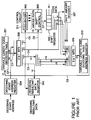
- variable length code decoding circuit includes a 20-bit variable length code decoding table 301, a 14-bit decoding start address register 304 receiving a 14-bit decoding start address, a "2 to 1" 20-bit multiplexor (2-input/1-output selector, or "1-out-of 2" selector) 309 receiving an output signal C1 of the variable length code decoding table 301 and an output signal C2 of the decoding start address register 304, a 16-bit decoding resultant data register 303 receiving the most significant 16 bits (output signal C3) of the output of the "2 to 1" multiplexor 309 and controlled by the least significant one bit (output signal C5) of the output of the "2 to 1" multiplexor 309, a sequencer 302 controlled by the output signal C5, a shift control circuit 305 and a shifting magnitude decoder 307 both of which receive the most significant
- Figure 2 illustrates a structure of the variable length code decoding table 301.
- the variable length decoding table 301 includes a retrieval continuation designating portion of one bit, three bits of data representative of the shifting number immediately after completion of decoding, and three bits of an upper (block) address when the retrieval is to be continued.
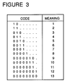
- Figure 3 shows one example of one group of variable length codes.
- Figures 4A, 4B and 4C are state transition diagrams at the time of decoding the variable length code shown in Figure 3, in units of two bits, three bits or four bits.
- Figures 5, 6 and 7 illustrate variable length code decoding tables corresponding to the state transition diagrams shown in Figures 4A, 4B and 4C.
- Figure 8 is a timing chart when the variable length code decoding table shown in Figure 5 is used to decode the code shown in Figure 3 in accordance with the state transition diagram shown in Figure 4A.
- Figure 9 is an example of the decoding table for decoding the variable length code for the 16-bit code in the prior art example now under examination, this table corresponding to the example of the timing chart shown in Figure 8.
- the decoding is advanced by tracing the code shown in Figure 3 from the left side in units of two bits.
- circles shown in Figure 4A indicate an initial state and an intermediate state in the decoding procedure.
- the decoding procedure is started from the leftmost circle, and if the first two bits in the decoding procedure are "00", the branch labelled "00" is traced, and if the first two bits are "01", the branch labelled "01" is traced.
- the meaning corresponding to the codes shown in Figure 3 is decoded.
- the branch "0X” means both the branch "00” and the branch "01".
- "X" means "don't care", namely, is a sign of a redundancy.
- Figure 4B illustrates the decoding procedure of advancing the decoding by tracing the code shown in Figure 3 from the left side in units of three bits.
- Figure 4C illustrates the decoding procedure of advancing the decoding by tracing the code shown in Figure 3 from the left side in units of four bits.
- the decoding table shown in Figure 5 is the table obtained by realizing the state transition shown in Figure 4A.
- the left column shows an access address for a next table when the decoding is in the intermediate state, and indicates which of the branches in the state transition diagram shown in Figure 4A should be traced.
- the left column shows the meaning of the decoded code (a positive integer in this example).
- the central column in Figure 5 is a field designating that when the decoding is completed, the shifting amount of the code is to be changed at the time of the decoding.
- "2" means the shifting of two bits
- "1" means the shifting of one bit.
- the code table shown in Figure 3 is retrieved in units of two bits in accordance with the state transition diagram shown in Figure 4A.
- the meaning of the code determined by retrieving the two bits in Figure 3 is only “1” and "2", and by further retrieving the two bits, the meaning of the codes corresponding to "3", "4", "5", “6” and “7” can be determined.
- "10" means a second address (address 2). Since the meaning of this code is determined, it is necessary to store "1" (as data) at the second address in the variable length code decoding table.
- the effective data is two bits, the decoding is completed by putting "0" in the retrieval continuation designating portion in order to cause the decoding to be completed after the shifting of two bits.
- the decoding table prepared to correspond to the decoding procedure of decoding the code in units of three bits as shown in Figure 4B is the decoding table shown in Figure 6
- the decoding table prepared to correspond to the decoding procedure of decoding the code in units of three bits as shown in Figure 4C is the decoding table shown in Figure 7.
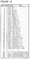
- the decoding table shown in Figure 9 and the code table shown in Figure 10 are decoding and code tables actually prepared in this manner, respectively. Accordingly, Figure 9 is a table corresponding to the variable length codes shown in the table of Figure 10.
- the decoding table shown in Figure 9 includes four fields, and is used to perform the decoding by use of the conventional example shown in Figure 1.
- the field 1 indicates a row (or line) number (including "0")
- the field 3 represents the amount of the shifting of the input data train to be shifted before the next retrieval.
- the field 4 is a flag showing whether or not the decoding is completed at their row (or line). "0" indicates the completion, and "1" indicates the incompletion.
- variable length code decoding circuit shown in Figure 1 has been proposed by JP-A-06-051943 referred to hereinbefore.
- the decoding start address signal C2 supplied from the decoding start address register 304 receiving the decoding start address the most significant 10 bits of the 14 bits are an address, and therefore, it is possible to modify the decoding start address signal C2.
- the decoding start address is set in the decoding start address register 304, and then, supplied through the "2 to 1" multiplexor 309.
- An intermediate data field of the decoding start address is supplied to the shift amount decoder 307 as the selection signal for the "3 to 1" multiplexor 308.
- the address signal of 12 bits for the variable length code decoding table 301 is generated.
- the variable length code decoding table 301 having the structure shown in Figure 2 is loaded with any one of the decoding tables shown in Figures 5,6,7 and 9, in order to cause the variable length code decoding circuit shown in Figure 1 to properly operate.
- the decoding start address and the code data are loaded to the decoding start address register 304 and the shift register 306, respectively.
- the most significant ten bits are the start address, and the shift amount to be retrieved and the retrieval continuation data is put in the least significant four bits.
- the code data in the shift register 306 is "00001X".
- "X" is a sign indicating the redundancy and the header of the next code, and therefore, "X" cannot be shifted out.
- the decoding start address C2 is outputted without modification from the "2 to 1" multiplexor 309.as the output signals C4, C5 and C6.
- the output signal C5 the start of the code retrieval is notified to the sequencer 302, and therefore, in response to this signal, the sequencer 302 generating various timing signals supplied to various parts, for controlling the start and the execution of the decoding operation.
- the data "00” is shifted out of the shift register 306 in accordance with the shift amount designated by the output signal C6 (the shifting out of two bits in this example), and this data "00” is supplied as the least significant two bits to the "3 to 1" multiplexor 308.
- the 10-bit data of the signal C4 "00 0000 0000” is supplied to the "3 to 1" multiplexor 308 as the most significant 10 bits. Therefore, the "3 to 1" multiplexor 308 outputs the 12-bit data "0000 0000 0000", which is in turn supplied to and stored in the variable length code decoding table address register 310. Accordingly, for the next address, the address of "000h” is supplied from the variable length code decoding table address register 310 as the signal C8 to the variable length code decoding table 301 for data retrieval (See Figure 5).
- variable length code decoding table 301 is outputted from the variable length code decoding table 301 as the decoding table output signal C1.
- the "2 to 1" multiplexor 309 outputs the signals C4, C5 and C6 at the timing t4 .
- the data "00” is shifted out of the shift register 306 in accordance with the shift amount designated by the output signal C6 (the shifting out of two bits in this example), and this data "00” is supplied as the least significant two bits to the "3 to 1" multiplexor 308.
- the 10-bit data of the signal C4 "00 0000 0001" is supplied to the "3 to 1" multiplexor 308 as the most significant 10 bits. Therefore, the "3 to 1" multiplexor 308 outputs the 12-bit data "0000 0000 0100", which is in turn supplied to and stored in the variable length code decoding table address register 310. Accordingly, for the next address, the address of "004h” is supplied from the variable length code decoding table address register 310 as the signal C8 to the variable length code decoding table 301 for data retrieval (See Figure 5).
- variable length code decoding table 301 is outputted from the variable length code decoding table 301 as the decoding table output signal C1.
- the "2 to 1" multiplexor 309 outputs the signals C4, C5 and C6.
- the data "1X” is shifted out of the shift register 306 in accordance with the shift amount designated by the output signal C6 (the shifting out of two bits in this example), and this data "1X” is supplied as the least significant two bits to the "3 to 1" multiplexor 308.
- the 10-bit data of the signal C4 "00 0000 0011” is supplied to the "3 to 1" multiplexor 308 as the most significant 10 bits. Therefore, the "3 to 1" multiplexor 308 outputs the 12-bit data "0000 0000 111X", which is in turn supplied to and stored in the variable length code decoding table address register 310.
- variable length code decoding table address register 310 the address of "00Eh” or "00Fh” having the redundancy is supplied from the variable length code decoding table address register 310 as the signal C8 to the variable length code decoding table 301 for data retrieval (See Figure 5).
- variable length code decoding table 301 is outputted from the variable length code decoding table 301 as the decoding table output signal C1.
- the "2 to 1" multiplexor 309 outputs the signals C4, C5 and C6.
- variable length code decoding circuit it is possible to reduce the number of retrieval cycles by increasing the number of bits included in each one unit to be retrieved.
- the decoding table basically becomes large by increasing the number of bits included in each one unit to be retrieved. Namely, the retrieval in units of two bits requires “17h” addresses (24 words) for the decoding table, and the retrieval in units of three bits requires “27h” addresses (40 words) for the decoding table. In addition, the retrieval in units of four bits requires "1Fh" addresses (32 words) for the decoding table. This is attributable to the fact that if the variable length codes have pattern extremely similar to each other, the variable length code decoding table becomes redundant.
- the bit length to be processed is increased from 8 bits to 9 bits, and therefore, the processing cycles is basically increased.
- variable length code decoding circuit which has overcome the above mentioned defect of the conventional one.
- Another object of the present invention is to provide a variable length code decoding circuit having a reduced size of a variable length code decoding table and capable of easily decoding the variable length code.
- variable length code decoding circuit comprising: a variable length code decoding table; a first memory means receiving and storing a decoding start address; a first selecting means receiving an output signal of the variable length code decoding table 101 and an output signal of the first memory means so as to output one selected output signal; a shift register receiving and storing a sequence of variable length codes to be decoded; a control means receiving the least significant "n" bits of the one selected output signal (where “n” is any positive integer), for controlling a bit shift amount of the shift register; a second selecting means receiving a portion of the code data stored in the shift register and the least significant "k” bits of the most significant "m” bits of the one selected output signal (where “k” and “m” are any positive integer and “k” is not greater than “m”), for outputting a synthesized address signal; a second memory means receiving and storing the synthesized address signal, for supplying the stored synthesized address signal to
- the positive/negative inversion circuit directly receives one of the most significant bit and the least significant bit of the code data stored in the shift register, for discriminating a positive/negative of a decoding resultant data signal, and for outputting, as the decoding resultant data signal, either the received content of the third memory means without modification or an inverted data of the received content of the third memory means.
- the positive/negative inversion circuit directly receives through the shift register a positive/negative discriminating bit generated by shifting the processing end signal, for discriminating a positive/negative of a decoding resultant data signal, and for outputting, as the decoding resultant data signal, either the received content of the third memory means without modification or an inverted data of the received content of the third memory means.
- control means includes a sequencer receiving the least significant bit of the least significant "n" bits of the one selected output signal, for controlling an operating timing of the decoding operation, and a shift control circuit receiving some most significant bits of the least significant "n” bits of the one selected output signal, for controlling a bit shift operation of the shift register.
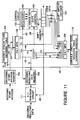
- variable length code decoding circuit in accordance with the present invention.
- the shown variable length code decoding circuit includes a 20-bit variable length code decoding table 101, a 14-bit decoding start address register 104 receiving a 14-bit decoding start address, a "2 to 1" 20-bit multiplexor 109 receiving an output signal A1 of the variable length code decoding table 101 and an output signal A2 of the decoding start address register 104, a 16-bit decoding resultant data register 103 receiving the most significant 16 bits (output signal A3) of the 20-bit output of the "2 to 1" multiplexor 109 and controlled by the least significant one bit (output signal A5) of the 20-bit output of the "2 to 1" multiplexor 109, a sequencer 102 controlled by the output signal A5, a shift control circuit 105 and a shifting magnitude decoder 107 both of which receive the most significant three bits (output signal A6) of the least significant four bits of the 20-bit output of the "2 to 1" multiplexor 109, a shift register 106 receiving and storing a bit sequence of continuous variable
- the sequencer 102 receives the output signal A5 from the "2 to 1" multiplexor 109, and generates various timing signals to be supplied to various parts in the circuit for determining the start, the execution and the end of the decoding operation.
- the decoding start address signal A2 supplied from the decoding start address register 104 receiving the decoding start address the most significant 10 bits of the 14 bits are an address, and therefore, it is possible to modify the decoding start address signal A2.
- the positive/negative inversion circuit 111 If the value of the most significant one bit A9 of the output signal outputted from the shift register 106 at the time of the completion of the decoding operation, is "1", the positive/negative inversion circuit 111 outputs, as the decoding resultant data, a 2'complement of the data supplied from the decoding resultant data register 103. If the most significant one bit A9 is "0”, the positive/negative inversion circuit 111 outputs, as the decoding resultant data, the data supplied from the decoding resultant data register 103, without modification.
- the decoding resultant data to be outputted from the positive/negative inversion circuit 111 is generated by simply adding the value of the most significant one bit A9 of the output signal outputted from the shift register 106 at the time of the completion of the decoding operation, to the most or least significant bit position of the data supplied from the decoding resultant data register 103.
- Figure 14 is table of variable length codes added with a sign bit.
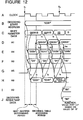
- Figure 12 is a timing chart illustrating the operation of the embodiment shown in Figure 11 on the basis of the variable length code table shown in Figure 14.
- the last bit (sign bit) in the variable length code table shown in Figure 14 is supplied to the positive/negative inversion circuit 111 as the most significant bit A9 outputted from the shift register 106 at the time of the completion of the decoding operation, and is processed only in the positive/negative inversion circuit 111. Accordingly, it is possible to omit the sign bit from the code table subjected to an actual decoding processing. Therefore, the decoding table for the variable length code table shown in Figure 14 becomes the-same as those shown in Figures 5, 6 and 7.
- Figure 12 is a timing chart illustrating the operation of the first embodiment.
- the decoding start address and the code data are loaded to the decoding start address register 104 and the shift register 106, respectively.
- the most significant 10 bits are the start address, and the least significant four bits indicate the shift amount to be retrieved and the retrieval continuation data.
- the code data in the shift register 106 is "00001S”
- "S" is not only a sign indicating the redundancy but also the header of the next code, and therefore, "S" cannot be shifted out.
- the sign bit is located in the position of this "S" according to the table of Figure 4, but in this embodiment, this "S” is processed as a simple redundant bit, not as the sign bit, similarly to the conventional variable length code decoding circuit, and thereafter, the bit "S" is separately processed after the completion of the conventional variable length code decoding processing.
- the decoding start address A2 is outputted without modification from the "2 to 1" multiplexor 109.as the output signals A4, A5 and A6. With the output signal A5, the start of the code retrieval is notified to the sequencer 102, and therefore, in response to this signal, the sequencer 102 generating various timing signals supplied to various parts, for controlling the start and the execution of the decoding operation.
- the data "00” is shifted out of the shift register 106 in accordance with the shift amount designated by the output signal A6 (the shifting out of two bits in this example), and this data "00” is supplied as the least significant two bits to the "3 to 1" multiplexor 108.
- the 10-bit data "00 0000 0000” of the signal A4 is supplied to the "3 to 1" multiplexor 108 as the most significant 10 bits. Therefore, the "3 to 1" multiplexor 108 outputs the 12-bit data "0000 0000 0000", which is in turn supplied to and stored in the variable length code decoding table address register 110. Accordingly, for the next address, the address of "000h" is supplied from the variable length code decoding table address register 110 as the signal A8 to the variable length code decoding table 101 for data retrieval (See Figure 5).
- variable length code decoding table 101 is outputted from the variable length code decoding table 101 as the decoding table output signal A1, and supplied to the "2 to 1" multiplexor 109, which in turn outputs the signals A4, A5 and A6 at the timing t4 .
- the data "00” is shifted out of the shift register 106 in accordance with the shift amount designated by the output signal A6 (the shifting out of two bits in this example), and this data "00” is supplied as the least significant two bits to the "3 to 1" multiplexor 108.
- the 10-bit data "00 0000 0001" of the signal A4 is supplied to the "3 to 1" multiplexor 108 as the most significant 10 bits. Therefore, the "3 to 1" multiplexor 108 outputs the 12-bit data "0000 0000 0100", which is in turn supplied to and stored in the variable length code decoding table address register 110. Accordingly, for the next address, the address of "004h” is supplied from the variable length code decoding table address register 110 as the signal A8 to the variable length code decoding table 101 for data retrieval (See Figure 5).
- variable length code decoding table 101 is outputted from the variable length code decoding table 101 as the decoding table output signal A1.
- the "2 to 1" multiplexor 109 outputs the signals A4, A5 and A6.
- the data "1S” is shifted out of the shift register 106 in accordance with the shift amount designated by the output signal A6 (the shifting out of two bits in this example), and this data "1S” is supplied as the least significant two bits to the "3 to 1" multiplexor 108.
- the 10-bit data "00 0000 0011" of the signal A4 is supplied to the "3 to 1" multiplexor 108 as the most significant 10 bits. Therefore, the "3 to 1" multiplexor 108 outputs the 12-bit data "0000 0000 111S", which is in turn supplied to and stored in the variable length code decoding table address register 110. Accordingly, for the next address, the address of "00Eh” or "00Fh” having the redundancy is supplied from the variable length code decoding table address register 110 as the signal A8 to the variable length code decoding table 101 for data retrieval (See Figure 5).
- variable length code decoding table 101 is outputted from the variable length code decoding table 101 as the decoding table output signal A1.
- the "2 to 1" multiplexor 109 outputs the signals A4, A5 and A6.
- the sign bit (positive/negative discriminating bit) remains at the most significant bit position of the shift register 106.
- This sign bit is supplied as the signal A9 to the positive/negative inversion circuit 111. Accordingly, on the basis of the sign bit of the signal A9, the data supplied from the decoding resultant data register 103 is subjected to the positive/negative inversion processing. In this case, the above mentioned data "0008h" is outputted as the decoding resultant data. Thus, the decoding operation is completed.
- the code data supplied to the shift register 106 is sequentially decoded.
- the decoding operation based on the retrieval in units of three bits or in units of four bits can be performed in accordance with the tables shown in Figures 6 and 7.
- the most significant three bits (output signal A6) of the least significant four bits of the 20-bit output of the "2 to 1" multiplexor 109 indicate the two-bit shifting. Namely, if the output signal A6 of the "2 to 1" multiplexor 109 indicates the two-bit shift, the shift control circuit 105 receiving the output signal A6 controls the shift register 106 so as to shift out the content of the shift register 106 in units of two bits, and the shifting magnitude decoder 107 also receiving the output signal A6 controls the "3 to 1" multiplexor 108 in such a manner that the 12-bit variable length code decoding table address is constituted of the most significant two bits of the shift register 106 and the least significant ten bits (output signal A4) of the output signal A3.
- the shift control circuit 105 controls the shift register 106 so as to shift out the content of the shift register 106 in units of three bits, and the shifting magnitude decoder 107 controls the "3 to 1" multiplexor 108 in such a manner that the 12-bit variable length code decoding table address is constituted of the most significant three bits of the shift register 106 and the most significant nine bits of the output signal A4 (ten bits).
- the shift control circuit 105 controls the shift register 106 so as to shift out the content of the shift register 106 in units of four bits, and the shifting magnitude decoder 107 controls the "3 to 1" multiplexor 108 in such a manner that the 12-bit variable length code decoding table address is constituted of the most significant four bits of the shift register 106 and the most significant eight bits of the output signal A4 (ten bits).
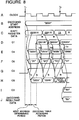
- FIG. 13 there is shown a diagram of a second embodiment of the variable length code decoding circuit in accordance with the present invention.
- the shown variable length code decoding circuit includes a 20-bit variable length code decoding table 201, a 14-bit decoding start address register 204 receiving a 14-bit decoding start address, a "2 to 1" 20-bit multiplexor 209 receiving an output signal B1 of the variable length code decoding table 201 and an output signal B2 of the decoding start address register 204, a 16-bit decoding resultant data register 203 receiving the most significant 16 bits (output signal B3) of the 20-bit output of the "2 to 1" multiplexor 209 and controlled by the least significant one bit (output signal B5) of the 20-bit output of the "2 to 1" multiplexor 209, a sequencer 202 controlled by the output signal B5, a shift control circuit 205 and a shifting magnitude decoder 207 both of which receive the most significant three bits (output signal B6) of the least significant four bits of the 20-bit output of the "2 to 1" multiplexor 209, a shift register 206 receiving the code data and controlled by an output
- the second embodiment is different from the first embodiment only in that, in the first embodiment, the most significant bit of the shift register 106 is supplied directly to the positive/negative inversion circuit 111, but in the second embodiment, after the decoding operation is completed, the sequencer 202 discriminates the end signal, and the shift register 106 is further shifted one bit so that the content of the shift register is used as the positive/negative discriminating data to the positive/negative inversion circuit 211 in the form of a signal B9.
- variable length code decoding circuit in accordance with the present invention is characterized by providing the positive/negative inversion circuit which directly receives the most significant bit of the shift register receiving the code data. Therefore, for the variable length code data accompanying the sign bit, the positive/negative discriminating processing can be performed independently of the decoding processing.
- the size of the variable length code decoding table becomes large and the data length of the codes increased one bit, it is possible to avoid the drop of the decoding processing, which would be occur because of the increase in the number of the decoding processing cycles.
- variable length code decoding circuit in accordance with the present invention can be used for a color moving image compress technology in accordance with the MPEGI of the ISO standard. Furthermore, it is possible to handle an image larger than the MPEGI of the ISO standard.
Landscapes
- Engineering & Computer Science (AREA)
- Theoretical Computer Science (AREA)
- Compression, Expansion, Code Conversion, And Decoders (AREA)
Applications Claiming Priority (3)
| Application Number | Priority Date | Filing Date | Title |
|---|---|---|---|
| JP105323/94 | 1994-05-19 | ||
| JP6105323A JP2604546B2 (ja) | 1994-05-19 | 1994-05-19 | 可変長符号の復号化処理装置 |
| JP10532394 | 1994-05-19 |
Publications (3)
| Publication Number | Publication Date |
|---|---|
| EP0683569A2 true EP0683569A2 (fr) | 1995-11-22 |
| EP0683569A3 EP0683569A3 (fr) | 1997-04-16 |
| EP0683569B1 EP0683569B1 (fr) | 2001-11-07 |
Family
ID=14404513
Family Applications (1)
| Application Number | Title | Priority Date | Filing Date |
|---|---|---|---|
| EP95107755A Expired - Lifetime EP0683569B1 (fr) | 1994-05-19 | 1995-05-19 | Circuit de décodage pour codes à longueur variable |
Country Status (4)
| Country | Link |
|---|---|
| US (1) | US5682156A (fr) |
| EP (1) | EP0683569B1 (fr) |
| JP (1) | JP2604546B2 (fr) |
| DE (2) | DE69523664T4 (fr) |
Cited By (1)
| Publication number | Priority date | Publication date | Assignee | Title |
|---|---|---|---|---|
| EP1069691A1 (fr) * | 1999-06-15 | 2001-01-17 | STMicroelectronics S.r.l. | Méthode de décodage de code de Huffman |
Families Citing this family (5)
| Publication number | Priority date | Publication date | Assignee | Title |
|---|---|---|---|---|
| KR0164097B1 (ko) * | 1995-06-15 | 1999-01-15 | 조백제 | 병렬 입력 / 직렬 출력 장치 및 그 방법 |
| US5835035A (en) * | 1995-12-28 | 1998-11-10 | Philips Electronics North America Corporation | High performance variable length decoder with two-word bit stream segmentation and related method |
| JP2000207205A (ja) * | 1999-01-14 | 2000-07-28 | Sony Corp | 演算装置 |
| US8913667B2 (en) * | 1999-11-09 | 2014-12-16 | Broadcom Corporation | Video decoding system having a programmable variable-length decoder |
| US6285303B1 (en) * | 2000-05-12 | 2001-09-04 | Eurica Califorrniaa | Gate table data compression and recovery process |
Citations (1)
| Publication number | Priority date | Publication date | Assignee | Title |
|---|---|---|---|---|
| EP0582273A2 (fr) | 1992-08-03 | 1994-02-09 | Nec Corporation | Circuit de décodage pour code à longueur variable |
Family Cites Families (3)
| Publication number | Priority date | Publication date | Assignee | Title |
|---|---|---|---|---|
| US4150368A (en) * | 1977-07-07 | 1979-04-17 | International Telephone And Telegraph Corporation | Signal coding for compressed pulse code modulation system |
| US4580129A (en) * | 1983-11-14 | 1986-04-01 | Northern Telecom Limited | Variable word length decoder |
| US5233348A (en) * | 1992-03-26 | 1993-08-03 | General Instrument Corporation | Variable length code word decoder for use in digital communication systems |
-
1994
- 1994-05-19 JP JP6105323A patent/JP2604546B2/ja not_active Expired - Fee Related
-
1995
- 1995-05-19 DE DE69523664T patent/DE69523664T4/de not_active Expired - Lifetime
- 1995-05-19 US US08/444,861 patent/US5682156A/en not_active Expired - Fee Related
- 1995-05-19 EP EP95107755A patent/EP0683569B1/fr not_active Expired - Lifetime
- 1995-05-19 DE DE69523664A patent/DE69523664D1/de not_active Expired - Fee Related
Patent Citations (3)
| Publication number | Priority date | Publication date | Assignee | Title |
|---|---|---|---|---|
| EP0582273A2 (fr) | 1992-08-03 | 1994-02-09 | Nec Corporation | Circuit de décodage pour code à longueur variable |
| JPH0651943A (ja) | 1992-08-03 | 1994-02-25 | Nec Corp | 可変長符号の復号化回路 |
| US5398027A (en) | 1992-08-03 | 1995-03-14 | Nec Corporation | Decoding circuit for variable length code |
Cited By (2)
| Publication number | Priority date | Publication date | Assignee | Title |
|---|---|---|---|---|
| EP1069691A1 (fr) * | 1999-06-15 | 2001-01-17 | STMicroelectronics S.r.l. | Méthode de décodage de code de Huffman |
| US6404358B1 (en) | 1999-06-15 | 2002-06-11 | Stmicroelectronics S.R.L. | Decoding method for a Huffman code |
Also Published As
| Publication number | Publication date |
|---|---|
| EP0683569A3 (fr) | 1997-04-16 |
| DE69523664T2 (de) | 2002-08-01 |
| EP0683569B1 (fr) | 2001-11-07 |
| JP2604546B2 (ja) | 1997-04-30 |
| DE69523664T4 (de) | 2003-01-30 |
| US5682156A (en) | 1997-10-28 |
| JPH07312556A (ja) | 1995-11-28 |
| DE69523664D1 (de) | 2001-12-13 |
Similar Documents
| Publication | Publication Date | Title |
|---|---|---|
| US5351047A (en) | Data decoding method and apparatus | |
| US5625355A (en) | Apparatus and method for decoding variable-length code | |
| EP0535571A2 (fr) | Système de codage/décodage de Huffman modifié avec un décodage simplifié pour les systèmes d'images | |
| US5550542A (en) | Variable length code look-up table having separate code length determination | |
| JP2002522821A (ja) | データプロセッサとデータ処理方法 | |
| JP3688297B2 (ja) | ビデオ画像カラーエンコーディング | |
| US5907635A (en) | Picture data decompression apparatus | |
| KR20000076123A (ko) | 부호화방법, 부호화장치 및 기록매체와, 복호화방법, 복호화장치 및 기록매체 | |
| KR100486251B1 (ko) | 가변 길이 코드 복호화 장치 및 방법 | |
| EP0582273B1 (fr) | Circuit de décodage pour code à longueur variable | |
| JP2007037115A (ja) | デジタルデータを符号化する方法、データセグメントのストリームを符号化する方法、エンコーダ、データのソースを符号化するためのパラレルエンコーダ、符号化データのソースを復号するためのパラレルデコーダ、コード化データを復号する方法、磁気テープドライブ、およびデータのストリームを符号化する方法 | |
| EP0683569A2 (fr) | Circuit de décodage pour codes à longueur variable | |
| US5701125A (en) | Method for compression of data using single pass LZSS and run-length encoding | |
| KR100339772B1 (ko) | 데이터화일들의압축및압축해제방법 | |
| US5309156A (en) | Variable-length code decoding device | |
| US5479626A (en) | Signal processor contexts with elemental and reserved group addressing | |
| US7676527B2 (en) | Processor | |
| JP2715871B2 (ja) | 可変長符号化方法 | |
| JPH08316847A (ja) | 可変長符号の復号装置 | |
| EP0499225B1 (fr) | Dispositif de décodage pour code à longueur variable | |
| JP3034293B2 (ja) | 可変長符号の固定長変換回路 | |
| CN1061765C (zh) | 数据移位控制电路 | |
| CA1208786A (fr) | Compression de donnees | |
| KR20010058369A (ko) | 코드길이에 따른 허프만 코드 복호장치 및 방법 | |
| JP3409845B2 (ja) | 可変長ビット列処理装置及びこれを用いた可変長ビット列処理方法 |
Legal Events
| Date | Code | Title | Description |
|---|---|---|---|
| PUAI | Public reference made under article 153(3) epc to a published international application that has entered the european phase |
Free format text: ORIGINAL CODE: 0009012 |
|
| AK | Designated contracting states |
Kind code of ref document: A2 Designated state(s): DE FR GB |
|
| PUAL | Search report despatched |
Free format text: ORIGINAL CODE: 0009013 |
|
| AK | Designated contracting states |
Kind code of ref document: A3 Designated state(s): DE FR GB |
|
| 17P | Request for examination filed |
Effective date: 19970721 |
|
| 17Q | First examination report despatched |
Effective date: 20000302 |
|
| GRAG | Despatch of communication of intention to grant |
Free format text: ORIGINAL CODE: EPIDOS AGRA |
|
| GRAG | Despatch of communication of intention to grant |
Free format text: ORIGINAL CODE: EPIDOS AGRA |
|
| GRAH | Despatch of communication of intention to grant a patent |
Free format text: ORIGINAL CODE: EPIDOS IGRA |
|
| GRAH | Despatch of communication of intention to grant a patent |
Free format text: ORIGINAL CODE: EPIDOS IGRA |
|
| GRAA | (expected) grant |
Free format text: ORIGINAL CODE: 0009210 |
|
| AK | Designated contracting states |
Kind code of ref document: B1 Designated state(s): DE FR GB |
|
| REF | Corresponds to: |
Ref document number: 69523664 Country of ref document: DE Date of ref document: 20011213 |
|
| REG | Reference to a national code |
Ref country code: GB Ref legal event code: IF02 |
|
| ET | Fr: translation filed | ||
| PLBE | No opposition filed within time limit |
Free format text: ORIGINAL CODE: 0009261 |
|
| STAA | Information on the status of an ep patent application or granted ep patent |
Free format text: STATUS: NO OPPOSITION FILED WITHIN TIME LIMIT |
|
| 26N | No opposition filed | ||
| REG | Reference to a national code |
Ref country code: GB Ref legal event code: 732E |
|
| REG | Reference to a national code |
Ref country code: FR Ref legal event code: TP |
|
| PGFP | Annual fee paid to national office [announced via postgrant information from national office to epo] |
Ref country code: DE Payment date: 20080522 Year of fee payment: 14 |
|
| PGFP | Annual fee paid to national office [announced via postgrant information from national office to epo] |
Ref country code: GB Payment date: 20080521 Year of fee payment: 14 |
|
| GBPC | Gb: european patent ceased through non-payment of renewal fee |
Effective date: 20090519 |
|
| REG | Reference to a national code |
Ref country code: FR Ref legal event code: ST Effective date: 20100129 |
|
| PG25 | Lapsed in a contracting state [announced via postgrant information from national office to epo] |
Ref country code: FR Free format text: LAPSE BECAUSE OF NON-PAYMENT OF DUE FEES Effective date: 20090602 |
|
| PGFP | Annual fee paid to national office [announced via postgrant information from national office to epo] |
Ref country code: FR Payment date: 20080514 Year of fee payment: 14 |
|
| PG25 | Lapsed in a contracting state [announced via postgrant information from national office to epo] |
Ref country code: GB Free format text: LAPSE BECAUSE OF NON-PAYMENT OF DUE FEES Effective date: 20090519 |
|
| PG25 | Lapsed in a contracting state [announced via postgrant information from national office to epo] |
Ref country code: DE Free format text: LAPSE BECAUSE OF NON-PAYMENT OF DUE FEES Effective date: 20091201 |