EP0684645A2 - Blindage contre interférences électromagnétiques pour un boîtier de circuit intégré - Google Patents
Blindage contre interférences électromagnétiques pour un boîtier de circuit intégré Download PDFInfo
- Publication number
- EP0684645A2 EP0684645A2 EP95300554A EP95300554A EP0684645A2 EP 0684645 A2 EP0684645 A2 EP 0684645A2 EP 95300554 A EP95300554 A EP 95300554A EP 95300554 A EP95300554 A EP 95300554A EP 0684645 A2 EP0684645 A2 EP 0684645A2
- Authority
- EP
- European Patent Office
- Prior art keywords
- heat sink
- package
- electrically conductive
- emf
- leadframe
- Prior art date
- Legal status (The legal status is an assumption and is not a legal conclusion. Google has not performed a legal analysis and makes no representation as to the accuracy of the status listed.)
- Withdrawn
Links
Images


Classifications
-
- H—ELECTRICITY
- H10—SEMICONDUCTOR DEVICES; ELECTRIC SOLID-STATE DEVICES NOT OTHERWISE PROVIDED FOR
- H10W—GENERIC PACKAGES, INTERCONNECTIONS, CONNECTORS OR OTHER CONSTRUCTIONAL DETAILS OF DEVICES COVERED BY CLASS H10
- H10W70/00—Package substrates; Interposers; Redistribution layers [RDL]
- H10W70/40—Leadframes
- H10W70/464—Additional interconnections in combination with leadframes
- H10W70/468—Circuit boards
-
- H—ELECTRICITY
- H10—SEMICONDUCTOR DEVICES; ELECTRIC SOLID-STATE DEVICES NOT OTHERWISE PROVIDED FOR
- H10W—GENERIC PACKAGES, INTERCONNECTIONS, CONNECTORS OR OTHER CONSTRUCTIONAL DETAILS OF DEVICES COVERED BY CLASS H10
- H10W40/00—Arrangements for thermal protection or thermal control
- H10W40/70—Fillings or auxiliary members in containers or in encapsulations for thermal protection or control
- H10W40/77—Auxiliary members characterised by their shape
- H10W40/778—Auxiliary members characterised by their shape in encapsulations
-
- H—ELECTRICITY
- H10—SEMICONDUCTOR DEVICES; ELECTRIC SOLID-STATE DEVICES NOT OTHERWISE PROVIDED FOR
- H10W—GENERIC PACKAGES, INTERCONNECTIONS, CONNECTORS OR OTHER CONSTRUCTIONAL DETAILS OF DEVICES COVERED BY CLASS H10
- H10W42/00—Arrangements for protection of devices
- H10W42/20—Arrangements for protection of devices protecting against electromagnetic or particle radiation, e.g. light, X-rays, gamma-rays or electrons
-
- H—ELECTRICITY
- H10—SEMICONDUCTOR DEVICES; ELECTRIC SOLID-STATE DEVICES NOT OTHERWISE PROVIDED FOR
- H10W—GENERIC PACKAGES, INTERCONNECTIONS, CONNECTORS OR OTHER CONSTRUCTIONAL DETAILS OF DEVICES COVERED BY CLASS H10
- H10W70/00—Package substrates; Interposers; Redistribution layers [RDL]
- H10W70/60—Insulating or insulated package substrates; Interposers; Redistribution layers
- H10W70/67—Insulating or insulated package substrates; Interposers; Redistribution layers characterised by their insulating layers or insulating parts
- H10W70/68—Shapes or dispositions thereof
- H10W70/682—Shapes or dispositions thereof comprising holes having chips therein
-
- H—ELECTRICITY
- H10—SEMICONDUCTOR DEVICES; ELECTRIC SOLID-STATE DEVICES NOT OTHERWISE PROVIDED FOR
- H10W—GENERIC PACKAGES, INTERCONNECTIONS, CONNECTORS OR OTHER CONSTRUCTIONAL DETAILS OF DEVICES COVERED BY CLASS H10
- H10W72/00—Interconnections or connectors in packages
- H10W72/50—Bond wires
- H10W72/541—Dispositions of bond wires
- H10W72/5449—Dispositions of bond wires not being orthogonal to a side surface of the chip, e.g. fan-out arrangements
-
- H—ELECTRICITY
- H10—SEMICONDUCTOR DEVICES; ELECTRIC SOLID-STATE DEVICES NOT OTHERWISE PROVIDED FOR
- H10W—GENERIC PACKAGES, INTERCONNECTIONS, CONNECTORS OR OTHER CONSTRUCTIONAL DETAILS OF DEVICES COVERED BY CLASS H10
- H10W72/00—Interconnections or connectors in packages
- H10W72/851—Dispositions of multiple connectors or interconnections
- H10W72/874—On different surfaces
- H10W72/884—Die-attach connectors and bond wires
-
- H—ELECTRICITY
- H10—SEMICONDUCTOR DEVICES; ELECTRIC SOLID-STATE DEVICES NOT OTHERWISE PROVIDED FOR
- H10W—GENERIC PACKAGES, INTERCONNECTIONS, CONNECTORS OR OTHER CONSTRUCTIONAL DETAILS OF DEVICES COVERED BY CLASS H10
- H10W90/00—Package configurations
- H10W90/701—Package configurations characterised by the relative positions of pads or connectors relative to package parts
- H10W90/731—Package configurations characterised by the relative positions of pads or connectors relative to package parts of die-attach connectors
- H10W90/736—Package configurations characterised by the relative positions of pads or connectors relative to package parts of die-attach connectors between a chip and a stacked lead frame, conducting package substrate or heat sink
-
- H—ELECTRICITY
- H10—SEMICONDUCTOR DEVICES; ELECTRIC SOLID-STATE DEVICES NOT OTHERWISE PROVIDED FOR
- H10W—GENERIC PACKAGES, INTERCONNECTIONS, CONNECTORS OR OTHER CONSTRUCTIONAL DETAILS OF DEVICES COVERED BY CLASS H10
- H10W90/00—Package configurations
- H10W90/701—Package configurations characterised by the relative positions of pads or connectors relative to package parts
- H10W90/751—Package configurations characterised by the relative positions of pads or connectors relative to package parts of bond wires
- H10W90/756—Package configurations characterised by the relative positions of pads or connectors relative to package parts of bond wires between a chip and a stacked lead frame, conducting package substrate or heat sink
Definitions
- the present invention relates to the housing and protection of integrated circuit chips. More specifically, the present invention relates to a package that provides electromagnetic field (EMF) shielding and thermal protection for integrated circuit chips.
- EMF electromagnetic field
- Modern integrated circuits require protection from self-heating effects, electromagnetic fields, electrostatic discharge, and mechanical shock in order to operate properly.
- the integrated circuit (IC) itself could be a source of EMF emissions that could be potentially harmful to other electronic devices in close proximity to the IC, or that could result in a violation of FCC regulations regarding EMF emissions.
- Barker package Another limitation of the Barker package is that it is not possible to house both EMF-generating components and EMF-sensitive components simultaneously in the same package. The reason for this is that this package does not provide an option for shielding two or more components from each other if they are mounted in the same package. If an EMF-generating component is mounted inside this package, then the only EMF-sensitive components that are protected from EMF emissions are those that are mounted outside the package. Conversely, if an EMF-sensitive component is mounted inside the package, then it will only be protected from EMF emissions emanating from electronic devices disposed outside the package.
- the present invention seeks to provide a package for housing one or more integrated circuits which will protect these integrated circuits from EMF emissions and thermal shock and also shield other electrical devices and the environment in general from EMF emissions, while still conforming to an industry recognized package outline.
- the heat sink contains a recess and is positioned against the conductive layer with the recess facing the conductive layer.
- the integrated circuit (IC) resides inside the cavity formed by the heat sink and conductive layer and is protected from EMF by the heat sink and conductive layer.
- these improvements are achieved by attaching a standard leadframe, which includes a leadframe paddle and lead fingers, to an electrically conductive heat sink that contains a recess.
- the heat sink is attached to the leadframe with the recess facing the leadframe and is electrically isolated from the leadframe, except for a ground connection, by using an electrically insulating material, such as electrically insulating adhesive or tape. This arrangement forms a cavity within the recess of the heat sink.
- the integrated circuit resides inside this cavity and is electrically insulated from the heat sink.
- the electrical leads on the IC are connected to the lead fingers with wire bonds. The lead fingers then become, in effect, extensions of the IC leads.
- an electrically conductive layer is attached to the side of the leadframe opposite the heat sink.
- This electrically conductive layer must be electrically isolated from the IC in order to achieve EMF shielding.
- the electrically conductive layer must be electrically isolated from the leadframe, except for a ground connection, to avoid shorting out the lead fingers. This electrical isolation can be accomplished by either using electrically insulating adhesive to attach the electrically conductive layer or by sandwiching the electrically conductive layer between two insulating layers before attaching it to the leadframe.
- the combination of the heat sink and electrically conductive layer substantially shields the IC from EMF.
- the EMF shielding is not 100% because there is the potential for EMF to reach the IC through the gap between the heat sink and the leadframe. Effective EMF protection is still achieved, however, because the gap thickness accounts for only about 10% of the total thickness for the heat sink and electrically conductive layer combination.
- Heat sinking is achieved by a thermal connection between the heat sink and the IC.
- the heat sink serves as both a thermal conductor and a component of the EMF shield.
- Additional ICs can housed by attaching them to the side of the electrically conductive layer opposite the leadframe. As with the IC mounted inside the cavity, these additional ICs must be electrically isolated from the electrically conductive layer attached to the leadframe. If the electrically conductive layer is sandwiched between two electrically insulating layers as discussed above, then the additional ICs can be attached directly to the electrically insulating layer. Otherwise, electrically insulating adhesive can be used. These additional ICs are protected from EMF emanating from the IC that is housed inside the cavity. This allows for the possibility of housing EMF-generating components and EMF-sensitive components in the same package.
- the heat sink, leadframe, electrically conductive layer, and ICs are then encapsulated in an electrically insulating molding compound.
- the compound is molded to an industry recognized package outline, such as those recognized by JEDEC or EIJA, which will make it possible for the package to be handled by the auto-insertion equipment that is typically used by board assemblers.
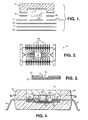
- FIG. 1 illustrates the basic principles of the invention.
- the basic principle involved in providing EMF shielding for an IC 8 is to surround the IC 8 with electrically conductive material that is electrically grounded. Although the IC 8 needs to be surrounded by electrically conductive material, the IC 8 cannot be in electrical contact with the electrically conductive material because, otherwise, EMF will be coupled to the IC 8.
- this EMF shielding concept is implemented with an electrically conductive heat sink 10 on one side of the IC, and an electrically conductive layer 12 on the other side of the IC.
- the heat sink 10 contains a recess 11 and is attached to a standard leadframe 14, which includes a leadframe paddle 16 and lead fingers 18, with the recess facing the leadframe 14.
- a plan view of the leadframe 14 is provided in FIG. 2.
- the heat sink 10 is electrically isolated from the lead fingers 18, except at a point where a ground connection is made between the heat sink 10 and a lead finger 18 that is connected to ground. This keeps the heat sink 10 from shorting out the lead fingers 18.
- This electrical isolation is provided by using an electrically insulating layer 20, such as an electrically insulating adhesive, gel or tape, between the heat sink 10 and the lead fingers 18.
- An opening in the insulating layer 20 over the lead finger 18 that is connected to ground allows for a ground connection to the heat sink 10.
- the IC 8 resides within the recess 11 of the heat sink 10.
- the leadframe paddle 16 may be removed, depending upon where the IC 8 is mounted. For example, if the IC 8 is attached directly to the heat sink 10, then the leadframe paddle 16 is not used. The IC 8 is then attached to the heat sink 10 before the electrically conductive layer 12 is attached. If the IC 8 is attached to the leadframe paddle 14, it is attached to the leadframe paddle 16 before the heat sink 10 and leadframe 14 are attached together.
- the electrically conductive layer 12 which is preferably formed from copper about 0.0254 mm thick, is attached to the side of the leadframe 14 opposite the heat sink 10. As with the heat sink 10, the electrically conductive layer 12 must be electrically isolated from the lead fingers 18, except at a point where a ground connection is made between the electrically conductive layer 10 and a lead finger 18 that is connected to ground, to avoid shorting the lead fingers 18 together. This can be accomplished by sandwiching the electrically conductive layer 12 between two electrically insulating layers 22. FIG. 3 provides a detailed view of this arrangement. An opening 24 in the electrically insulating layer 22 over the grounded lead finger 18 allows for a ground connection to the electrically conductive layer 12.
- FIG. 4 illustrates the various elements of the invention assembled together in the preferred embodiment.
- the entire assembly is encapsulated in an electrically insulating molding compound 34 such that the lead fingers 18 extend beyond the boundaries of the molding compound 34.
- the molding compound 34 is molded to an industry recognized package outline, such as those recognized by the Joint Electron Device Engineering Council (JEDEC) or the Electronics Industry Association of Japan (EIJA), which will make it possible for the package to be handled by the auto-insertion equipment that is typically used by board assemblers.
- JEDEC Joint Electron Device Engineering Council
- EIJA Electronics Industry Association of Japan
- the upper surface of the heat sink 10 is flush with the upper surface of the molding compound for this purpose.
- the IC 8 is substantially protected from EMF emissions, however, the protection is not 100% because of the existence of gaps in the electrically conductive "shield" formed by the heat sink 10 and the electrically conductive layer 12. These gaps are located at the electrically insulating layer 20 between the heat sink 10 and the lead fingers 18 and at the electrically insulating layer 22 between the lead fingers 18 and the electrically conductive layer 12. Effective EMF protection is still achieved, however, because the gap thickness accounts for only about 10% of the total thickness for the heat sink 10 and electrically conductive layer 12 combination.
- a thermal path is provided by making a thermal connection between the IC 8 and the heat sink 10.
- the heat sink 10 serves as both a component of the EMF shield and as a thermal conductor.
- the IC 8 is attached to the leadframe paddle 16 with thermally conductive and electrically insulating adhesive 26 before the heat sink 10 is attached to the leadframe 14.
- a thermally conductive gel 28 such as high thermal conductivity silicone, is placed between the IC 8 and the heat sink 10 before the heat sink 10 is attached to the leadframe 14.
- Heat spreaders 30 are simply extensions of the leadframe paddle 16, as shown in FIG. 5. Since the leadframe 14 is typically made of thermally conductive material, such as copper, and since the IC 8 is attached to the leadframe paddle with a thermally conductive and electrically insulating adhesive 26, these heat spreaders conduct heat away from the IC 8. Thermal connections between the heat spreaders 30 and the heat sink 10 can then be made at locations where the heat sink 10 is directly above a heat spreader 30. These connections can be accomplished by either making the electrically insulating layer 20 thermally conductive, such as by using polyimide tape or adhesive, or by providing openings in the electrically insulating layer 20 where the heat sink 10 is directly above a heat spreader 30.
- FIG. 6 illustrates an embodiment in which the IC 8 is mounted directly to the heat sink 10 with a thermally conductive but electrically insulating adhesive 36.
- the leadframe paddle 16 is not used in this configuration.
- the IC 8 is then attached to the heat sink 10. In this configuration, heat is directly transferred to the heat sink 10 and is dissipated, while electrical isolation is maintained between the heat sink 10 and the IC 8.
- FIGS. 7 and 8 illustrate embodiments in which additional ICs 38 are housed in the package outside the EMF shielded enclosure. These ICs 38 are protected from EMF emissions emanating from the IC 8 inside the EMF shielded enclosure. This embodiment, therefore, allows for the packaging of EMF-generating components and EMF-sensitive components in the same package.
- the IC 8 inside the enclosure can be an EMF-generating component and the ICs 38 outside the enclosure can be EMF-sensitive components.
- the additional ICs 38 are preferably attached to the electrically insulating layer 22 located at the bottom of the electrically conductive layer 12 with thermally conductive but electrically insulating adhesive 39. Electrically conductive tracks 43 are incorporated into the electrically insulating layer 22 upon which the additional ICs are mounted. Electrical connections between the IC 38 leads and the lead fingers 18 are made by connecting the IC 38 leads to the conductive tracks 43 with wire bonds 40, and connecting the conductive tracks 43 to the lead fingers 18 with additional wire bonds 41.
- a thermal path for the additional ICs 38 is provided by metal feedthroughs 42 that extend from the ICs 38 through the electrically insulating layers 22 and electrically conductive layer 12 to the heat spreaders 30.
- the IC 8 inside the enclosure is mounted to the heat sink as in FIG. 1.
- the leadframe paddle 16 has been removed and the IC 8 inside the enclosure is attached to the electrically insulating layer 22 that faces the heat sink 10.
- the leads on the IC 8 inside the enclosure can then be connected to the lead fingers 18 using the same wire bonding method used for connecting the leads on the additional ICs 38 to the lead fingers 18.
- a thermal path for the IC 8 may be achieved by using the same thermally conductive gel 28 as in FIG. 1.
- a heat spreader 30, as described earlier and shown in FIG. 5 can be used by incorporating thermally conductive tracks on the electrically insulating layer 22 on which the IC 8 is mounted. These thermally conductive tracks are thermally connected to the heat sink 10 using the same technique described earlier for the heat spreaders 30.
Landscapes
- Cooling Or The Like Of Semiconductors Or Solid State Devices (AREA)
- Structures Or Materials For Encapsulating Or Coating Semiconductor Devices Or Solid State Devices (AREA)
Applications Claiming Priority (2)
| Application Number | Priority Date | Filing Date | Title |
|---|---|---|---|
| US250166 | 1994-05-26 | ||
| US08/250,166 US5486720A (en) | 1994-05-26 | 1994-05-26 | EMF shielding of an integrated circuit package |
Publications (2)
| Publication Number | Publication Date |
|---|---|
| EP0684645A2 true EP0684645A2 (fr) | 1995-11-29 |
| EP0684645A3 EP0684645A3 (fr) | 1998-02-11 |
Family
ID=22946558
Family Applications (1)
| Application Number | Title | Priority Date | Filing Date |
|---|---|---|---|
| EP95300554A Withdrawn EP0684645A3 (fr) | 1994-05-26 | 1995-01-30 | Blindage contre interférences électromagnétiques pour un boítier de circuit intégré |
Country Status (2)
| Country | Link |
|---|---|
| US (1) | US5486720A (fr) |
| EP (1) | EP0684645A3 (fr) |
Cited By (3)
| Publication number | Priority date | Publication date | Assignee | Title |
|---|---|---|---|---|
| DE102007002156A1 (de) * | 2007-01-15 | 2008-07-17 | Infineon Technologies Ag | Halbleiteranordnung mit Wärmesenke |
| EP1858080A3 (fr) * | 2006-05-16 | 2008-11-05 | Broadcom Corporation | Emballages de circuit imprimé sans fil dotés d'un dissipateur thermique pour le blindage contre les interférences électromagnétiques et l'amélioration thermique |
| DE102023136713A1 (de) | 2023-12-27 | 2025-07-03 | Infineon Technologies Ag | Package mit einer komponententragenden Zwischenstruktur und einem zusätzlichen Träger, der eine Referenzpotentialstruktur aufweist |
Families Citing this family (64)
| Publication number | Priority date | Publication date | Assignee | Title |
|---|---|---|---|---|
| US6911727B1 (en) | 1995-06-06 | 2005-06-28 | Analog Devices, Inc. | Package for sealing an integrated circuit die |
| US6323550B1 (en) * | 1995-06-06 | 2001-11-27 | Analog Devices, Inc. | Package for sealing an integrated circuit die |
| US5739581A (en) * | 1995-11-17 | 1998-04-14 | National Semiconductor Corporation | High density integrated circuit package assembly with a heatsink between stacked dies |
| US5644167A (en) * | 1996-03-01 | 1997-07-01 | National Semiconductor Corporation | Integrated circuit package assemblies including an electrostatic discharge interposer |
| US6795120B2 (en) * | 1996-05-17 | 2004-09-21 | Sony Corporation | Solid-state imaging apparatus and camera using the same |
| US5798570A (en) * | 1996-06-28 | 1998-08-25 | Kabushiki Kaisha Gotoh Seisakusho | Plastic molded semiconductor package with thermal dissipation means |
| US6159764A (en) * | 1997-07-02 | 2000-12-12 | Micron Technology, Inc. | Varied-thickness heat sink for integrated circuit (IC) packages and method of fabricating IC packages |
| US5986209A (en) * | 1997-07-09 | 1999-11-16 | Micron Technology, Inc. | Package stack via bottom leaded plastic (BLP) packaging |
| US6168975B1 (en) * | 1998-06-24 | 2001-01-02 | St Assembly Test Services Pte Ltd | Method of forming extended lead package |
| US6326687B1 (en) * | 1998-09-01 | 2001-12-04 | Micron Technology, Inc. | IC package with dual heat spreaders |
| JP2000114413A (ja) * | 1998-09-29 | 2000-04-21 | Sony Corp | 半導体装置、その製造方法および部品の実装方法 |
| US6583987B2 (en) * | 1999-02-26 | 2003-06-24 | Intel Corporation | Electromagnetic interference and heatsinking |
| US6052045A (en) * | 1999-03-12 | 2000-04-18 | Kearney-National, Inc. | Electromechanical switching device package with controlled impedance environment |
| US6215180B1 (en) * | 1999-03-17 | 2001-04-10 | First International Computer Inc. | Dual-sided heat dissipating structure for integrated circuit package |
| DE19914815A1 (de) * | 1999-03-31 | 2000-10-05 | Abb Research Ltd | Halbleitermodul |
| US6211565B1 (en) * | 1999-04-29 | 2001-04-03 | Winbond Electronics Corporation | Apparatus for preventing electrostatic discharge in an integrated circuit |
| US6198163B1 (en) * | 1999-10-18 | 2001-03-06 | Amkor Technology, Inc. | Thin leadframe-type semiconductor package having heat sink with recess and exposed surface |
| USRE38381E1 (en) | 2000-07-21 | 2004-01-13 | Kearney-National Inc. | Inverted board mounted electromechanical device |
| US6538304B1 (en) * | 2000-11-16 | 2003-03-25 | Texas Instruments Incorporated | Corner bonding to lead frame |
| US6515861B1 (en) * | 2001-04-02 | 2003-02-04 | Advanced Micro Devices, Inc. | Method and apparatus for shielding electromagnetic emissions from an integrated circuit |
| NL1018243C2 (nl) * | 2001-06-08 | 2002-12-10 | Oce Tech Bv | Printhead voor een beeldvormend apparaat en beeldvormend apparaat voorzien van een dergelijk printhead. |
| US7176506B2 (en) * | 2001-08-28 | 2007-02-13 | Tessera, Inc. | High frequency chip packages with connecting elements |
| US6856007B2 (en) * | 2001-08-28 | 2005-02-15 | Tessera, Inc. | High-frequency chip packages |
| US6396130B1 (en) | 2001-09-14 | 2002-05-28 | Amkor Technology, Inc. | Semiconductor package having multiple dies with independently biased back surfaces |
| TW517365B (en) * | 2001-11-29 | 2003-01-11 | Orient Semiconductor Elect Ltd | Heat dissipation plate and its bonding process with substrate |
| DK1483769T3 (da) * | 2002-03-08 | 2008-01-28 | Kearney National Inc | Stöbt relæenhed til overflademontering og fremgangsmåde til fremstilling af denne |
| US6747870B2 (en) | 2002-04-25 | 2004-06-08 | Gateway, Inc. | Electromagnetic interference reduction air duct |
| US7754537B2 (en) * | 2003-02-25 | 2010-07-13 | Tessera, Inc. | Manufacture of mountable capped chips |
| US6972480B2 (en) | 2003-06-16 | 2005-12-06 | Shellcase Ltd. | Methods and apparatus for packaging integrated circuit devices |
| WO2005004195A2 (fr) * | 2003-07-03 | 2005-01-13 | Shellcase Ltd. | Procede et appareil d'encapsulation de circuits integres |
| US7298030B2 (en) * | 2003-09-26 | 2007-11-20 | Tessera, Inc. | Structure and method of making sealed capped chips |
| US20050067681A1 (en) * | 2003-09-26 | 2005-03-31 | Tessera, Inc. | Package having integral lens and wafer-scale fabrication method therefor |
| US7009106B2 (en) * | 2003-10-09 | 2006-03-07 | Bosch Security Systems, Inc. | Shielding assembly and method |
| US20050139984A1 (en) * | 2003-12-19 | 2005-06-30 | Tessera, Inc. | Package element and packaged chip having severable electrically conductive ties |
| US20050189635A1 (en) * | 2004-03-01 | 2005-09-01 | Tessera, Inc. | Packaged acoustic and electromagnetic transducer chips |
| TWI240423B (en) * | 2004-03-12 | 2005-09-21 | Opto Tech Corp | Light emitting device with high heat dissipation efficiency |
| US8143095B2 (en) * | 2005-03-22 | 2012-03-27 | Tessera, Inc. | Sequential fabrication of vertical conductive interconnects in capped chips |
| JP4538359B2 (ja) * | 2005-03-31 | 2010-09-08 | 株式会社日立産機システム | 電気回路モジュール |
| US7582951B2 (en) * | 2005-10-20 | 2009-09-01 | Broadcom Corporation | Methods and apparatus for improved thermal performance and electromagnetic interference (EMI) shielding in leadframe integrated circuit (IC) packages |
| TWI284407B (en) * | 2005-11-03 | 2007-07-21 | Cyntec Co Ltd | Package device with electromagnetic interference shield |
| US20070190747A1 (en) * | 2006-01-23 | 2007-08-16 | Tessera Technologies Hungary Kft. | Wafer level packaging to lidded chips |
| US7936062B2 (en) * | 2006-01-23 | 2011-05-03 | Tessera Technologies Ireland Limited | Wafer level chip packaging |
| US20080002460A1 (en) * | 2006-03-01 | 2008-01-03 | Tessera, Inc. | Structure and method of making lidded chips |
| US7714453B2 (en) * | 2006-05-12 | 2010-05-11 | Broadcom Corporation | Interconnect structure and formation for package stacking of molded plastic area array package |
| US7808087B2 (en) | 2006-06-01 | 2010-10-05 | Broadcom Corporation | Leadframe IC packages having top and bottom integrated heat spreaders |
| US8581381B2 (en) | 2006-06-20 | 2013-11-12 | Broadcom Corporation | Integrated circuit (IC) package stacking and IC packages formed by same |
| US8154881B2 (en) * | 2006-11-13 | 2012-04-10 | Telecommunication Systems, Inc. | Radiation-shielded semiconductor assembly |
| US8604605B2 (en) | 2007-01-05 | 2013-12-10 | Invensas Corp. | Microelectronic assembly with multi-layer support structure |
| US8183687B2 (en) * | 2007-02-16 | 2012-05-22 | Broadcom Corporation | Interposer for die stacking in semiconductor packages and the method of making the same |
| US7872335B2 (en) * | 2007-06-08 | 2011-01-18 | Broadcom Corporation | Lead frame-BGA package with enhanced thermal performance and I/O counts |
| WO2009008703A1 (fr) * | 2007-07-09 | 2009-01-15 | Innocleaning Magma Holding | Tête de balai à franges et procédé d'essuyage |
| CN101677092B (zh) * | 2008-09-18 | 2011-12-14 | 乾坤科技股份有限公司 | 芯片封装结构 |
| US8533853B2 (en) | 2009-06-12 | 2013-09-10 | Telecommunication Systems, Inc. | Location sensitive solid state drive |
| US8084300B1 (en) | 2010-11-24 | 2011-12-27 | Unisem (Mauritius) Holdings Limited | RF shielding for a singulated laminate semiconductor device package |
| US10636735B2 (en) * | 2011-10-14 | 2020-04-28 | Cyntec Co., Ltd. | Package structure and the method to fabricate thereof |
| WO2016053966A2 (fr) * | 2014-09-30 | 2016-04-07 | Henkel IP & Holding GmbH | Régulation de la température à l'aide de matériaux à changement de phase contenus dans un boîtier de protection contre les interférences électromagnétiques |
| DE102015219366B4 (de) | 2015-05-22 | 2024-02-22 | Volkswagen Aktiengesellschaft | Interposer und Halbleitermodul zur Anwendung in automobilen Applikationen |
| USD906271S1 (en) * | 2018-04-13 | 2020-12-29 | Rohm Co., Ltd. | Semiconductor module |
| USD937231S1 (en) * | 2020-04-06 | 2021-11-30 | Wolfspeed, Inc. | Power semiconductor package |
| USD1009818S1 (en) * | 2021-10-13 | 2024-01-02 | Rohm Co., Ltd. | Semiconductor device |
| JP1711418S (ja) * | 2021-10-13 | 2022-03-31 | 半導体素子 | |
| USD1037187S1 (en) * | 2022-05-12 | 2024-07-30 | Alpha And Omega Semiconductor International Lp | Power semiconductor module |
| USD1042375S1 (en) * | 2022-05-12 | 2024-09-17 | Alpha And Omega Semiconductor International Lp | Power semiconductor module |
| USD1107671S1 (en) * | 2022-05-12 | 2025-12-30 | Alpha And Omega Semiconductor International Lp | Power semiconductor module |
Family Cites Families (14)
| Publication number | Priority date | Publication date | Assignee | Title |
|---|---|---|---|---|
| US3902148A (en) * | 1970-11-27 | 1975-08-26 | Signetics Corp | Semiconductor lead structure and assembly and method for fabricating same |
| US4829403A (en) * | 1987-01-20 | 1989-05-09 | Harding Ade Yemi S K | Packaging arrangement for energy dissipating devices |
| US5184211A (en) * | 1988-03-01 | 1993-02-02 | Digital Equipment Corporation | Apparatus for packaging and cooling integrated circuit chips |
| JPH0278752A (ja) * | 1988-09-16 | 1990-03-19 | Riken Corp | 内燃機関用アルミニウム合金製ピストン |
| JPH049650A (ja) * | 1990-04-26 | 1992-01-14 | Kubota Corp | 長尺物の撮像装置 |
| US5043534A (en) * | 1990-07-02 | 1991-08-27 | Olin Corporation | Metal electronic package having improved resistance to electromagnetic interference |
| US5297007A (en) * | 1990-09-19 | 1994-03-22 | Rockwell International Corporation | E/M shielded RF circuit board |
| JPH04152554A (ja) * | 1990-10-16 | 1992-05-26 | Hitachi Ltd | 半導体装置およびその実装体 |
| US5175613A (en) * | 1991-01-18 | 1992-12-29 | Digital Equipment Corporation | Package for EMI, ESD, thermal, and mechanical shock protection of circuit chips |
| US5172213A (en) * | 1991-05-23 | 1992-12-15 | At&T Bell Laboratories | Molded circuit package having heat dissipating post |
| JP3322429B2 (ja) * | 1992-06-04 | 2002-09-09 | 新光電気工業株式会社 | 半導体装置 |
| US5317107A (en) * | 1992-09-24 | 1994-05-31 | Motorola, Inc. | Shielded stripline configuration semiconductor device and method for making the same |
| US5371404A (en) * | 1993-02-04 | 1994-12-06 | Motorola, Inc. | Thermally conductive integrated circuit package with radio frequency shielding |
| US5294826A (en) * | 1993-04-16 | 1994-03-15 | Northern Telecom Limited | Integrated circuit package and assembly thereof for thermal and EMI management |
-
1994
- 1994-05-26 US US08/250,166 patent/US5486720A/en not_active Expired - Lifetime
-
1995
- 1995-01-30 EP EP95300554A patent/EP0684645A3/fr not_active Withdrawn
Cited By (4)
| Publication number | Priority date | Publication date | Assignee | Title |
|---|---|---|---|---|
| EP1858080A3 (fr) * | 2006-05-16 | 2008-11-05 | Broadcom Corporation | Emballages de circuit imprimé sans fil dotés d'un dissipateur thermique pour le blindage contre les interférences électromagnétiques et l'amélioration thermique |
| US8183680B2 (en) | 2006-05-16 | 2012-05-22 | Broadcom Corporation | No-lead IC packages having integrated heat spreader for electromagnetic interference (EMI) shielding and thermal enhancement |
| DE102007002156A1 (de) * | 2007-01-15 | 2008-07-17 | Infineon Technologies Ag | Halbleiteranordnung mit Wärmesenke |
| DE102023136713A1 (de) | 2023-12-27 | 2025-07-03 | Infineon Technologies Ag | Package mit einer komponententragenden Zwischenstruktur und einem zusätzlichen Träger, der eine Referenzpotentialstruktur aufweist |
Also Published As
| Publication number | Publication date |
|---|---|
| EP0684645A3 (fr) | 1998-02-11 |
| US5486720A (en) | 1996-01-23 |
Similar Documents
| Publication | Publication Date | Title |
|---|---|---|
| US5486720A (en) | EMF shielding of an integrated circuit package | |
| JP3407971B2 (ja) | 集積回路パッケージおよびその組立構造 | |
| JP4437919B2 (ja) | 電子部品パッケージ用emi遮蔽 | |
| US5796170A (en) | Ball grid array (BGA) integrated circuit packages | |
| US5710459A (en) | Integrated circuit package provided with multiple heat-conducting paths for enhancing heat dissipation and wrapping around cap for improving integrity and reliability | |
| US6515870B1 (en) | Package integrated faraday cage to reduce electromagnetic emissions from an integrated circuit | |
| US5581122A (en) | Packaging assembly with consolidated common voltage connections for integrated circuits | |
| US6011299A (en) | Apparatus to minimize integrated circuit heatsink E.M.I. radiation | |
| US6580167B1 (en) | Heat spreader with spring IC package | |
| EP0712160A2 (fr) | Améliorations dans ou relatives à des circuits intégrés | |
| US5525835A (en) | Semiconductor chip module having an electrically insulative thermally conductive thermal dissipator directly in contact with the semiconductor element | |
| US6562655B1 (en) | Heat spreader with spring IC package fabrication method | |
| US6943436B2 (en) | EMI heatspreader/lid for integrated circuit packages | |
| KR930004248B1 (ko) | 반도체소자패키지 및 반도체소자패키지 탑재배선회로기판 | |
| US20060001048A1 (en) | Power delivery using an integrated heat spreader | |
| KR0178567B1 (ko) | 반도체 집적회로용 플랫 패키지 | |
| KR100788858B1 (ko) | 집적 회로 패키지의 구조물 및 어셈블리 방법 | |
| NL8503487A (nl) | Verpakking voor geintegreerde schakelingen met verbeterde warmteafvoermogelijkheden, en werkwijze ter verbetering van de warmteafvoer. | |
| JP3506547B2 (ja) | 半導体装置 | |
| US5150198A (en) | Radiator for semiconductor chip | |
| KR20040063784A (ko) | 반도체장치 | |
| JPH06112674A (ja) | 電子部品搭載装置用のヒートシンク | |
| JPH1012675A (ja) | シールド付き表面実装部品 | |
| JPH0595055A (ja) | 半導体集積回路 | |
| US6563198B1 (en) | Adhesive pad having EMC shielding characteristics |
Legal Events
| Date | Code | Title | Description |
|---|---|---|---|
| PUAI | Public reference made under article 153(3) epc to a published international application that has entered the european phase |
Free format text: ORIGINAL CODE: 0009012 |
|
| AK | Designated contracting states |
Kind code of ref document: A2 Designated state(s): DE FR GB |
|
| PUAL | Search report despatched |
Free format text: ORIGINAL CODE: 0009013 |
|
| AK | Designated contracting states |
Kind code of ref document: A3 Designated state(s): DE FR GB |
|
| STAA | Information on the status of an ep patent application or granted ep patent |
Free format text: STATUS: THE APPLICATION IS DEEMED TO BE WITHDRAWN |
|
| 18D | Application deemed to be withdrawn |
Effective date: 19980812 |