EP0686979B1 - Dispositif de mémoire défaillant aux pannes, en particulier de type "flash EEPROM" - Google Patents
Dispositif de mémoire défaillant aux pannes, en particulier de type "flash EEPROM" Download PDFInfo
- Publication number
- EP0686979B1 EP0686979B1 EP94830283A EP94830283A EP0686979B1 EP 0686979 B1 EP0686979 B1 EP 0686979B1 EP 94830283 A EP94830283 A EP 94830283A EP 94830283 A EP94830283 A EP 94830283A EP 0686979 B1 EP0686979 B1 EP 0686979B1
- Authority
- EP
- European Patent Office
- Prior art keywords
- cells
- cell
- deletion
- accordance
- gain
- Prior art date
- Legal status (The legal status is an assumption and is not a legal conclusion. Google has not performed a legal analysis and makes no representation as to the accuracy of the status listed.)
- Expired - Lifetime
Links
Images

Classifications
-
- G—PHYSICS
- G11—INFORMATION STORAGE
- G11C—STATIC STORES
- G11C29/00—Checking stores for correct operation ; Subsequent repair; Testing stores during standby or offline operation
- G11C29/70—Masking faults in memories by using spares or by reconfiguring
- G11C29/78—Masking faults in memories by using spares or by reconfiguring using programmable devices
- G11C29/80—Masking faults in memories by using spares or by reconfiguring using programmable devices with improved layout
- G11C29/816—Masking faults in memories by using spares or by reconfiguring using programmable devices with improved layout for an application-specific layout
- G11C29/82—Masking faults in memories by using spares or by reconfiguring using programmable devices with improved layout for an application-specific layout for EEPROMs
-
- G—PHYSICS
- G11—INFORMATION STORAGE
- G11C—STATIC STORES
- G11C16/00—Erasable programmable read-only memories
- G11C16/02—Erasable programmable read-only memories electrically programmable
- G11C16/06—Auxiliary circuits, e.g. for writing into memory
- G11C16/34—Determination of programming status, e.g. threshold voltage, overprogramming or underprogramming, retention
-
- G—PHYSICS
- G11—INFORMATION STORAGE
- G11C—STATIC STORES
- G11C29/00—Checking stores for correct operation ; Subsequent repair; Testing stores during standby or offline operation
- G11C29/04—Detection or location of defective memory elements, e.g. cell constructio details, timing of test signals
- G11C29/50—Marginal testing, e.g. race, voltage or current testing
-
- G—PHYSICS
- G06—COMPUTING OR CALCULATING; COUNTING
- G06F—ELECTRIC DIGITAL DATA PROCESSING
- G06F2201/00—Indexing scheme relating to error detection, to error correction, and to monitoring
- G06F2201/81—Threshold
-
- G—PHYSICS
- G11—INFORMATION STORAGE
- G11C—STATIC STORES
- G11C16/00—Erasable programmable read-only memories
- G11C16/02—Erasable programmable read-only memories electrically programmable
- G11C16/04—Erasable programmable read-only memories electrically programmable using variable threshold transistors, e.g. FAMOS
-
- G—PHYSICS
- G11—INFORMATION STORAGE
- G11C—STATIC STORES
- G11C29/00—Checking stores for correct operation ; Subsequent repair; Testing stores during standby or offline operation
- G11C29/04—Detection or location of defective memory elements, e.g. cell constructio details, timing of test signals
- G11C29/50—Marginal testing, e.g. race, voltage or current testing
- G11C2029/5006—Current
Definitions
- the present invention relates to a memory device and in particular a flash EPROM in accordance with the preamble of claim 8 and a method for discriminating a gain-based insulated-gate single memorisation-transistor memory cell and to a method of deleting a memory cell of the same type.
- the memory device in accordance with the present invention can find advantageous application also in integrated circuits such as microprocessors and microcontrollers.
- the memory device In the area of non-volatile semiconductor memories, presently comprising the UV_EPROM, E_EPROM and flash EPROM, the memory device consists of a matrix of equal cells which comprise for the memorisation of the data a single MOS transistor having at least one insulated gate. The value 0 or 1 of the data memorised depends on the amount of charges present on the insulated gate which in turn determines the threshold voltage of the MOS transistor.
- redundant rows and/or one or more redundant columns are often provided in the matrix. These are used during manufacturing testing to obviate manufacturing defects by replacing the rows or columns containing faults with redundant rows or columns.
- a memory system having a two dimensional array of EEPROM or Flash EEPROM cells is known from the international patent application No. WO 94/07211 filed on September 1, 1993 in the name of Sundisk Corporation.
- Such a document describes a matrix of memory cells having a plurality of rows and columns, decoding means for row and/or column addresses, and a control logic for writing, reading and deletion of the cells, said control logic providing for the identification of cell faults in order to replace defective cells by good ones.
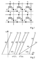
- FIG. 1 shows a flash EPROM cell matrix with 2 rows and 3 columns.
- the reading operation consists of applying to the selected cell a polarisation voltage (for writing) and detecting the corresponding current (for writing) and in comparing it with appropriate reference currents.
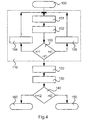
- FIG. 2 shows in a simplified manner the gate voltage versus channel current characteristics of cells having different charge status.
- A0 indicates the characteristic of a cell at instant t0 having a threshold voltage VT(t0) and gain G1 while A1 indicates the characteristic of the same cell at instant t1, following t0, after a deletion phase and thus having the same gain G1 but threshold voltage VT(t1) lower than VT(t0).
- the verification phase consists of a particular reading operation performed with particular reference currents more restrictive than those used for the normal reading operation.
- the characteristic indicated by A2 in FIG. 2 having a reference gain G represents the limit of the programming condition while after the subsequent deletion operation all the cells have a threshold voltage lower than a pre-set value VT1.
- the characteristic indicated by A3 in FIG. 2 having the same reference gain G represents the limit of the deletion condition.
- the values Vt0 and VT1 depend on the manufacturing process and design choices. A possible choice could be 5V for VT0 and 2V for VT1 respectively.
- A4 in FIG. 2 belongs to a cell of this type having gain G2. This phenomenon is found in manufacturing testing and during the life of the device and leads to the fact that when the deletion operation is terminated the cells having normal transconductance, i.e. nearly all, have reached extremely low threshold voltages often less than 0V. This leads to the shortcomings mentioned above and can also lead to degradation of a large part of the cell matrix. In addition it is also possible that the deletion operation will not end in the maximum time limits provided.
- the purpose of the present invention is to provide a method capable of identifying these situations during normal operation of the device and rectify them, in the light of the found and unexpected fact that they can arise even during the life of the device, and provide a memory device which would be tolerant of 'fault' situations like these and in particular gain lowering.
- the decoding means comprise at least one non-volatile memory for address mapping and that the control logic comprise means for identifying cell faults in the rows and/or columns of the matrix and writing means designed for writing on said non-volatile memory during normal operation addresses corresponding to the redundant rows and/or columns to rectify said faults.
- FIG. 3 shows a series of characteristics of cells all having different gains and a common point P1 identified by the co-ordinates V1,I1, i.e. by applying the reading voltage V1 to all these cells there is obtained therefrom the same reading current I1 and the characteristics are indicated in decreasing order of gain and threshold voltage by B0 (with gain G0 and threshold voltage VT(B0)), B1 (with gain G1 and threshold voltage VT(B1)), B2 (with gain G2 and threshold voltage VT(B2)) respectively.
- B0 with gain G0 and threshold voltage VT(B0)
- B1 with gain G1 and threshold voltage VT(B1)
- B2 with gain G2 and threshold voltage VT(B2)
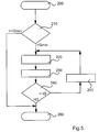
- the method in accordance with the present invention for discriminating on the basis of the gain a memory cell of the type with single insulated-gate memorisation transistor comprises the following phases:
- the second reading voltage V2 e.g. 6.25V, higher than the first reading voltage V1, e.g. 4.5V, the second value I2 higher than the first value I1, and the cell associated with a first class of high-gain cells if from said comparison it proved that said second reading current I(V2) was higher than said second value I2 and otherwise with a second low-gain cell class.
- the one shown in FIG. 3 could be the situation which appears in three cells of an EPROM flash memory device after phase a. of the method in accordance with the present invention.
- the second reading voltage V2 By applying to the three cells the second reading voltage V2 there will be detected the currents I(BO), I(B1), I(B2) respectively of which the first two are higher than the second value I2 while the last, i.e. I(B2), is not.
- the first two cells will be considered high-gain and the last low-gain. Graphically it can be seen that the characteristics slope reflects this situation.
- a conventional deletion operation of the cells of a memory device of the insulated-gate single-transistor memorisation type consists of at least one series of successive individual deletion and verification phases of the cell deletion status.
- the deletion method in accordance with the present invention comprises also at least one individual cell discrimination phase on the basis of the gain suitable for identifying the high-gain cells and provides that, after said discrimination phase, the individual verification phases affect only the high-gain cells.
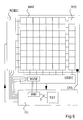
- the deletion method can be rapidly understood by considering the description given together with the flow chart shown in FIG. 5 and having the following block-actions correspondence and in which V3 and I3 indicate the voltage and current respectively on the basis of which the cell deletion condition is to be verified:
- the discrimination phase - block 210 - precedes the actual cell deletion.
- the discrimination phase can be provided by any method.
- the discrimination method in accordance with the present invention immediately after the 'preconditioning' and before the actual deletion because in this case, if a value of V1 lower than the value of VT0 is chosen, the discrimination phase already carries a partial but not dangerous deletion of the cells which thus shortens the actual deletion. As a whole then the deletion performed with the method of the present invention is not basically longer than that of the known art but considerably safer.
- the cells which are not high-gain are considered faulty and possibly signalled as such to the user of the device. In a very simple case the user will avoid using them.
- a more sophisticated version of the method provides that at least the faulty cells are replaced with redundant cells. More often it happens that the entire column or row to which they belong is replaced.
- the memory device also comprises means for applying a voltage to the gate terminal of cell, and means for detecting a current through the cell channel.
- the decoding means RDEC, CDEC comprise at least one non-volatile memory NVM for address mapping and the control logic CL comprises means TST designed to identify cell faults in the rows and/or columns and writing means WM designed to write on the non-volatile memory NVM, during normal operation of the device, addresses corresponding to said at least one redundant row and/or column RID to rectify said faults.
- FIG. 6 there is a matrix MAT made up of 8 rows and 8 columns, only one redundant column RID, a 3-bit row decoder RDEC, a 3-bit column decoder CDEC, and a non-volatile memory NVM formed from 8 3-bit words, used only for mapping column addresses and included in the 3-bit column decoder CDEC.
- From the control logic CL comes out the column address to be sent to the 3-bit column decoder CDEC, the row address to be sent to the 3-bit row decoder RDEC, and at least one signal DEL for the deletion to be sent to the matrix MAT. Furthermore it is connected to the input of the 3-bit row decoder RDEC and the input of the 3-bit column decoder CDEC.
- the means TST pilot the writing means WM which are connected in writing to the non-volatile memory NVM.
- non-volatile memory NVM contains in order the following eight words: 000, 001, 010, 011, 100, 101, 110, 111.
- the means TST When the means TST identify a 'fault' among those foreseen in a particular cell, they send to the writing means WM the column address corresponding to said faulty cell, e.g. 011.
- the writing means WM use this address to address the non-volatile memory NVM and use as writing data the column address corresponding to the redundancy column, in the example 111, and perform a writing operation on the non-volatile memory NVM.
- non-volatile memory NVM contains in order the following eight words: 000, 001, 010, 111, 100, 101, 110, 111.
- control logic CL which can be the wired or programmed type. For deletion, this can be pre-set to operate in accordance with the method of the present invention.
- the means TST can be in particular individual discrimination means for the cells of the matrix MAT which can consist of logics of the wired or programmed type and operate, e.g. in accordance with the method of the present invention.
- a fault tolerant memory device in accordance with the present invention can find an advantageous application in any integrated circuit where it is necessary to store data and/or programs.
Landscapes
- For Increasing The Reliability Of Semiconductor Memories (AREA)
- Read Only Memory (AREA)
Claims (11)
- Procédé en vue de discriminer une cellule de mémoire du type à mémorisation par grille isolée à un seul transistor, en fonction du gain, caractérisé en ce qu'il comprend les phases suivantes :a) porter la grille isolée de la cellule dans un état de charge de sorte qu'en appliquant une première tension de lecture (V1) à la borne de la grille de la cellule au moyen des phases successives de programmation et/ou de suppression et de vérification, un premier courant de lecture (I(V1)) est détecté dans le canal de la cellule sensiblement égal à une première valeur (I1),b) appliquer une seconde tension de lecture (V2) à la borne de la grille de la cellule, ladite seconde tension de lecture (V2) étant différente de ladite première tension de lecture (V1),c) détecter un second courant (I(V2)) dans le canal de la cellule correspondant à la seconde tension de lecture (V2),d) comparer la valeur du second courant de lecture (I(V2) à une seconde valeur (I2), ete) associer la cellule alternativement à une première ou une seconde classe de cellules en fonction du résultat de cette comparaison.
- Procédé selon la revendication 1 dans lequel ladite seconde tension de lecture (V2) est supérieure à ladite première tension de lecture (V1) et dans lequel ladite seconde valeur (I2) est supérieure à ladite première valeur (I1) et dans lequel ladite cellule est associée à une première classe de cellules à gain élevé si le résultat de cette comparaison prouve que ledit second courant de lecture (I(V2)) est supérieur à une seconde valeur (I2) et, autrement, est associée à une seconde classe de cellules à faible gain.
- Procédé selon la revendication 1, comprenant en outre au moins une série de phases successives de suppression et de vérification individuelle de l'état de suppression de la cellule, lesdites phases de vérification individuelles n'affectant que les cellules à gain élevé.
- Procédé selon la revendication 3 dans lequel ladite phase de discrimination a lieu selon le procédé décrit dans les revendications 1 ou 2 avant ladite série de phases successives de suppression et de vérification.
- Procédé selon la revendication 3 ou 4 dans lequel les cellules qui ne sont pas à gain élevé sont considérées comme défectueuses.
- Procédé selon la revendication 5 dans lequel au moins lesdites cellules défectueuses sont remplacées par des cellules redondantes.
- Procédé selon la revendication 6 dans lequel lesdites cellules redondantes connaissent en moyenne la même vie que les cellules qui ne sont pas redondantes avant ledit remplacement.
- Dispositif de mémoire du type comprenant :caractérisé en ce que ledit moyen de décodage (RDEC, CDEC) comprend au moins une mémoire non volatile (NVM) afin de mettre en correspnndance lesdites adresses et en ce que ladite logique de commande (CL) comprend un moyen (TST) conçu afin d'identifier les défauts de cellule dans lesdites lignes et/ou colonnes en comparant le gain des cellules et un moyen d'écriture (WM) conçu afin d'écrire sur ladite mémoire non volatile (NVM) des adresses correspondant à ladite ou les dites ligne et/ou colonne redondante (RID) en vue de rectifier lesdits défauts.a.) une matrice (MAT) de cellules de mémoire présentant une pluralité de lignes et de colonnes parmi lesquelles au moins une ligne et/ou une colonne (RID) est redondante,b.) un moyen de décodage (RDEC, CDEC) pour les adresses de lignes et/ou de colonnes,c.) une logique de commande (CL) afin d'écrire, lire et supprimer les cellules et commander les composants du dispositif,d.) un moyen en vue d'appliquer une tension à la borne de la grille de la cellule, ete.) un moyen en vue de détecter un courant dans le canal de la cellule,
- Dispositif selon la revendication 8 dans lequel ladite logique de commande (CL) comprend par ailleurs un moyen de discrimination (TST) pour lesdites cellules en fonction du gain et conçues afin de piloter ledit moyen d'écriture (WM).
- Dispositif selon la revendication 9 dans lequel la logique de commande (CL) fonctionne pour la suppression selon le procédé décrit dans l'une des revendications 3 à 7.
- Circuit intégré comprenant un dispositif de mémoire en vue de stocker des données et/ou des programmes caractérisé en ce que ledit dispositif de mémoire est du type décrit dans les revendications 8 à 10.
Priority Applications (4)
| Application Number | Priority Date | Filing Date | Title |
|---|---|---|---|
| DE69426818T DE69426818T2 (de) | 1994-06-10 | 1994-06-10 | Fehlertolerantes Speichergerät, insbesondere des Typs "flash EEPROM" |
| EP94830283A EP0686979B1 (fr) | 1994-06-10 | 1994-06-10 | Dispositif de mémoire défaillant aux pannes, en particulier de type "flash EEPROM" |
| US08/454,650 US5682349A (en) | 1994-06-10 | 1995-05-31 | Failure tolerant memory device, in particular of the flash EEPROM type |
| JP14503495A JP3725581B2 (ja) | 1994-06-10 | 1995-06-12 | セルの判別方法とその消去方法,および,それらの方法に用いられるメモリ・デバイスとそのメモリ・デバイスを用いた集積回路 |
Applications Claiming Priority (1)
| Application Number | Priority Date | Filing Date | Title |
|---|---|---|---|
| EP94830283A EP0686979B1 (fr) | 1994-06-10 | 1994-06-10 | Dispositif de mémoire défaillant aux pannes, en particulier de type "flash EEPROM" |
Publications (2)
| Publication Number | Publication Date |
|---|---|
| EP0686979A1 EP0686979A1 (fr) | 1995-12-13 |
| EP0686979B1 true EP0686979B1 (fr) | 2001-03-07 |
Family
ID=8218466
Family Applications (1)
| Application Number | Title | Priority Date | Filing Date |
|---|---|---|---|
| EP94830283A Expired - Lifetime EP0686979B1 (fr) | 1994-06-10 | 1994-06-10 | Dispositif de mémoire défaillant aux pannes, en particulier de type "flash EEPROM" |
Country Status (4)
| Country | Link |
|---|---|
| US (1) | US5682349A (fr) |
| EP (1) | EP0686979B1 (fr) |
| JP (1) | JP3725581B2 (fr) |
| DE (1) | DE69426818T2 (fr) |
Families Citing this family (12)
| Publication number | Priority date | Publication date | Assignee | Title |
|---|---|---|---|---|
| GB9614551D0 (en) | 1996-07-11 | 1996-09-04 | Memory Corp Plc | Memory system |
| US6532556B1 (en) | 2000-01-27 | 2003-03-11 | Multi Level Memory Technology | Data management for multi-bit-per-cell memories |
| US6314023B1 (en) * | 2000-06-15 | 2001-11-06 | Motorola, Inc. | Non-volatile programming elements for redundancy and identification in an integrated circuit |
| US6466476B1 (en) | 2001-01-18 | 2002-10-15 | Multi Level Memory Technology | Data coding for multi-bit-per-cell memories having variable numbers of bits per memory cell |
| DE60212332T2 (de) * | 2002-04-26 | 2007-06-06 | Stmicroelectronics S.R.L., Agrate Brianza | Selbstreparatur-Methode für nicht flüchtige Speicher mit einer Architektur zur Fehlervermeidung sowie nicht flüchtiger Speicher |
| DE60230592D1 (de) | 2002-05-21 | 2009-02-12 | St Microelectronics Srl | Selbstreparaturverfahren für nichtflüchtige Speicheranordnung mit Lösch-/Programmierfehlerdetektion, und nichtflüchtige Speicheranordnung dafür |
| US6839275B2 (en) * | 2003-06-04 | 2005-01-04 | Hewlett-Packard Development Company, L.P. | Memory system having control circuit configured to receive data, provide encoded received data to match a fault pattern in the array of memory cells |
| US7046555B2 (en) * | 2003-09-17 | 2006-05-16 | Sandisk Corporation | Methods for identifying non-volatile memory elements with poor subthreshold slope or weak transconductance |
| US7177189B2 (en) * | 2004-03-01 | 2007-02-13 | Intel Corporation | Memory defect detection and self-repair technique |
| JP2006294144A (ja) * | 2005-04-12 | 2006-10-26 | Toshiba Corp | 不揮発性半導体記憶装置 |
| WO2007036985A1 (fr) * | 2005-09-27 | 2007-04-05 | Advantest Corporation | Procédé de controle, et système de controle |
| US7545679B1 (en) * | 2007-12-28 | 2009-06-09 | Freescale Semiconductor, Inc. | Electrical erasable programmable memory transconductance testing |
Family Cites Families (11)
| Publication number | Priority date | Publication date | Assignee | Title |
|---|---|---|---|---|
| EP0198935A1 (fr) * | 1985-04-23 | 1986-10-29 | Deutsche ITT Industries GmbH | Mémoire redondante à semi-conducteur électriquement reprogrammable |
| JPS62114200A (ja) * | 1985-11-13 | 1987-05-25 | Mitsubishi Electric Corp | 半導体メモリ装置 |
| EP0403822B1 (fr) * | 1989-06-19 | 1994-10-12 | Texas Instruments Incorporated | Circuit et procédé pour le conditionnement d'EEPROMS remis à zéro avant la programmation |
| US5233559A (en) * | 1991-02-11 | 1993-08-03 | Intel Corporation | Row redundancy for flash memories |
| KR960002006B1 (ko) * | 1991-03-12 | 1996-02-09 | 가부시끼가이샤 도시바 | 2개의 기준 레벨을 사용하는 기록 검증 제어기를 갖는 전기적으로 소거 가능하고 프로그램 가능한 불휘발성 메모리 장치 |
| JP3080743B2 (ja) * | 1991-12-27 | 2000-08-28 | 日本電気株式会社 | 不揮発性半導体記憶装置 |
| KR960002777B1 (ko) * | 1992-07-13 | 1996-02-26 | 삼성전자주식회사 | 반도체 메모리 장치의 로우 리던던시 장치 |
| FR2694404B1 (fr) * | 1992-07-31 | 1994-09-09 | Sgs Thomson Microelectronics | Procédé de mesure des tensions de seuil des cellules d'une mémoire intégrée. |
| US5428621A (en) * | 1992-09-21 | 1995-06-27 | Sundisk Corporation | Latent defect handling in EEPROM devices |
| US5452251A (en) * | 1992-12-03 | 1995-09-19 | Fujitsu Limited | Semiconductor memory device for selecting and deselecting blocks of word lines |
| JP3212421B2 (ja) * | 1993-09-20 | 2001-09-25 | 富士通株式会社 | 不揮発性半導体記憶装置 |
-
1994
- 1994-06-10 EP EP94830283A patent/EP0686979B1/fr not_active Expired - Lifetime
- 1994-06-10 DE DE69426818T patent/DE69426818T2/de not_active Expired - Fee Related
-
1995
- 1995-05-31 US US08/454,650 patent/US5682349A/en not_active Expired - Lifetime
- 1995-06-12 JP JP14503495A patent/JP3725581B2/ja not_active Expired - Lifetime
Also Published As
| Publication number | Publication date |
|---|---|
| JPH0883500A (ja) | 1996-03-26 |
| JP3725581B2 (ja) | 2005-12-14 |
| DE69426818D1 (de) | 2001-04-12 |
| US5682349A (en) | 1997-10-28 |
| DE69426818T2 (de) | 2001-10-18 |
| EP0686979A1 (fr) | 1995-12-13 |
Similar Documents
| Publication | Publication Date | Title |
|---|---|---|
| US7437631B2 (en) | Soft errors handling in EEPROM devices | |
| US5532962A (en) | Soft errors handling in EEPROM devices | |
| EP0314180B1 (fr) | Mémoire non volatile à semi-conducteur comprenant un circuit de test en charge élevée | |
| US5659550A (en) | Latent defect handling in EEPROM devices | |
| CN100446121C (zh) | 半导体存储装置及其制造方法 | |
| US4733394A (en) | Electrically programmable semiconductor memory showing redundance | |
| US6646930B2 (en) | Non-volatile semiconductor memory | |
| US9070449B2 (en) | Defective block management | |
| KR0168896B1 (ko) | 패리티에 의해 에러를 수정할 수 있는 반도체 메모리장치 | |
| DE69426817T2 (de) | Fertigungprüfungsverfahren von Flash-EEPROM-Vorrichtungen | |
| EP0686979B1 (fr) | Dispositif de mémoire défaillant aux pannes, en particulier de type "flash EEPROM" | |
| DE10026993B4 (de) | Flash-Speicherbauelement mit einer neuen Redundanzansteuerschaltung | |
| DE102007016460A1 (de) | Nichtflüchtiges Speicherbauelement, nichtflüchtiges Speichersystem und Leseverfahren für ein nichtflüchtiges Speicherbauelement | |
| JPH06267300A (ja) | 不揮発性半導体記憶装置と半導体装置及びその試験方法 | |
| KR900006160B1 (ko) | 반도체 기억 장치 | |
| US20080285368A1 (en) | Method for nrom array word line retry erasing and threshold voltage recovering | |
| US6819589B1 (en) | Flash memory with pre-detection for data loss | |
| JPH07296592A (ja) | 不揮発性半導体記憶装置 | |
| JPH10228783A (ja) | 不揮発性半導体記憶装置とその動作方法 | |
| US7382660B2 (en) | Method for accessing a multilevel nonvolatile memory device of the flash NAND type | |
| US6850437B2 (en) | Nonvolatile semiconductor memory device and method of retrieving faulty in the same | |
| US20070025167A1 (en) | Method for testing a memory device, test unit for testing a memory device and memory device | |
| KR970017698A (ko) | 반도체 기억장치 및 그 용장 메모리셀부의 치환방법 | |
| US5594693A (en) | Matrix device with redundancy fuses for integrated memory | |
| JP3384409B2 (ja) | 書換え可能な不揮発性半導体記憶装置及びその制御方法 |
Legal Events
| Date | Code | Title | Description |
|---|---|---|---|
| PUAI | Public reference made under article 153(3) epc to a published international application that has entered the european phase |
Free format text: ORIGINAL CODE: 0009012 |
|
| AK | Designated contracting states |
Kind code of ref document: A1 Designated state(s): DE FR GB IT |
|
| 17P | Request for examination filed |
Effective date: 19960601 |
|
| 17Q | First examination report despatched |
Effective date: 19980529 |
|
| RAP3 | Party data changed (applicant data changed or rights of an application transferred) |
Owner name: STMICROELECTRONICS S.R.L. |
|
| GRAG | Despatch of communication of intention to grant |
Free format text: ORIGINAL CODE: EPIDOS AGRA |
|
| GRAG | Despatch of communication of intention to grant |
Free format text: ORIGINAL CODE: EPIDOS AGRA |
|
| GRAH | Despatch of communication of intention to grant a patent |
Free format text: ORIGINAL CODE: EPIDOS IGRA |
|
| GRAH | Despatch of communication of intention to grant a patent |
Free format text: ORIGINAL CODE: EPIDOS IGRA |
|
| GRAA | (expected) grant |
Free format text: ORIGINAL CODE: 0009210 |
|
| AK | Designated contracting states |
Kind code of ref document: B1 Designated state(s): DE FR GB IT |
|
| REF | Corresponds to: |
Ref document number: 69426818 Country of ref document: DE Date of ref document: 20010412 |
|
| ET | Fr: translation filed | ||
| ITF | It: translation for a ep patent filed | ||
| REG | Reference to a national code |
Ref country code: GB Ref legal event code: IF02 |
|
| PLBE | No opposition filed within time limit |
Free format text: ORIGINAL CODE: 0009261 |
|
| 26N | No opposition filed | ||
| PGFP | Annual fee paid to national office [announced via postgrant information from national office to epo] |
Ref country code: DE Payment date: 20030610 Year of fee payment: 10 |
|
| PGFP | Annual fee paid to national office [announced via postgrant information from national office to epo] |
Ref country code: GB Payment date: 20040602 Year of fee payment: 11 |
|
| PGFP | Annual fee paid to national office [announced via postgrant information from national office to epo] |
Ref country code: FR Payment date: 20040628 Year of fee payment: 11 |
|
| PG25 | Lapsed in a contracting state [announced via postgrant information from national office to epo] |
Ref country code: DE Free format text: LAPSE BECAUSE OF NON-PAYMENT OF DUE FEES Effective date: 20050101 |
|
| PG25 | Lapsed in a contracting state [announced via postgrant information from national office to epo] |
Ref country code: IT Free format text: LAPSE BECAUSE OF NON-PAYMENT OF DUE FEES;WARNING: LAPSES OF ITALIAN PATENTS WITH EFFECTIVE DATE BEFORE 2007 MAY HAVE OCCURRED AT ANY TIME BEFORE 2007. THE CORRECT EFFECTIVE DATE MAY BE DIFFERENT FROM THE ONE RECORDED. Effective date: 20050610 Ref country code: GB Free format text: LAPSE BECAUSE OF NON-PAYMENT OF DUE FEES Effective date: 20050610 |
|
| PG25 | Lapsed in a contracting state [announced via postgrant information from national office to epo] |
Ref country code: FR Free format text: LAPSE BECAUSE OF NON-PAYMENT OF DUE FEES Effective date: 20060228 |
|
| GBPC | Gb: european patent ceased through non-payment of renewal fee |
Effective date: 20050610 |
|
| REG | Reference to a national code |
Ref country code: FR Ref legal event code: ST Effective date: 20060228 |