EP0687370B1 - Verfahren und vorrichtung zur erkennung von optisch kodierten signalen - Google Patents
Verfahren und vorrichtung zur erkennung von optisch kodierten signalen Download PDFInfo
- Publication number
- EP0687370B1 EP0687370B1 EP94907651A EP94907651A EP0687370B1 EP 0687370 B1 EP0687370 B1 EP 0687370B1 EP 94907651 A EP94907651 A EP 94907651A EP 94907651 A EP94907651 A EP 94907651A EP 0687370 B1 EP0687370 B1 EP 0687370B1
- Authority
- EP
- European Patent Office
- Prior art keywords
- word
- optical
- words
- recognised
- pulse
- Prior art date
- Legal status (The legal status is an assumption and is not a legal conclusion. Google has not performed a legal analysis and makes no representation as to the accuracy of the status listed.)
- Expired - Lifetime
Links
Images



Definitions
- the present invention relates to a method and apparatus for processing optically encoded signals, and in particular to the recognition of an optically encoded binary word.
- w i and t i are the ith bits of the respective binary words and, as is customary in Boolean algebra, sums and products represent the OR and AND operations respectively, and x ⁇ (x bar)denotes the logical complement of x.
- the present inventor has realised that with an appropriate choice of codewords it is possible to carry out recognition entirely in the optical domain, using an optical AND operation.
- the encoding words are restricted to a sub-set of all the possible n-bit binary words and then word recognition is carried out using a method based entirely on AND operations at the bit level.
- the AND operation as represented by the simple scalar product of two optical fields, is a fundamental capability of many non-linear optical devices. Accordingly, it can be implemented far more straightforwardly than other logical operations, such as the exclusive-OR operation previously used for optical code word recognition.
- the process of word recognition is carried out in the optical domain with only the final discriminatory output being produced in the electrical domain.
- bit rate is not limited by the response time of the photodetector and electronics. This means that when, for example, the system is used to read the header in a very high speed optical packet, this can be done at the full bit rate of the packet.
- this process of recognition may be carried out at a switching node in which an incoming packet encoded in RTZ format, e.g. as solitons, is routed according to whether the packet address field H is equal to a local address A.
- a single optical pulse P which is in precise synchronism with the incoming packet may be generated and passed through a passive split-delay-recombine network which converts it to a pulse train representing A ⁇ (the binary logical complement of the local address A).
- the incoming packet header H and the pulse train A ⁇ are, in this example, incident simultaneously at an ultra fast optical AND gate.
- the output of the gate is zero only if H equals A. If H is not equal to A, then at least one optical pulse is obtained at the output of the optical AND gate. This output is detected (i.e. converted to the electrical domain) and may be used to control the routing switch. Only one optical AND gate is needed. No electrical summation or multi-level discrimination is needed. Since the output of the gate is immediately converted to the electrical domain, the gate need not be wavelength preserving, neither need it have high optical efficiency nor need it be cascadable. Any ultrafast non linear optical device yielding an output proportional to the scalar product of two input fields may be used.
- the non-linear optical device used to carry out the AND operation may, for example, be a SHG (second harmonic generator) crystal.
- SHG second harmonic generator
- other non-linear optical processes may be used, such as optical sum-frequency or difference-frequency mixing, harmonic generation, polarisation rotation using the optical Kerr effect, cross-phase modulation, degenerate four-wave mixing, or optical phase conjugation. All these non-linear optical phenomena produce an output proportional to the scalar product of two input optical signals.
- a variety of non-linear optical media may be used, such as crystals, semiconductors, organic materials or glasses. It may be particularly advantageous to use a non-linear optical medium in the form of an optical waveguide.
- the present invention is not limited to processing signals representing a time-series, such as the header of a packet on an optical network. It may also be used for pattern or image recognition, in which case the different bits of the binary word will be distributed in space rather than in time.
- the different bits W 1 , W 2 ...W i of the word then correspond to binary pixels, and the image is recognised by carrying out AND operations on the pixels in the optical domain with the complement of the binary target image.
- the code word W is provided with a datum pulse having a fixed, bit-asynchronous time relationship to the rest of the word, and the datum pulse is used in generating a pulse sequence T' dependent on the target word T.
- the word T' is generated by applying the word W including the datum pulse to a splitter/delay network, the different arms of the network having different respective delays determined depending upon the target word T.
- each code word is provided with an additional pulse which has a fixed time relationship to the code word pulse train but is bit-asynchronous with it.
- the datum pulse may occur 1.5 bit periods before the start of the header of a packet.
- This datum pulses is then used in generating a word related to the target word T for ANDing with the incoming code word. This may be done, for example, using a network which creates a signal including the logical complement T of the target word.
- an optical word recognition device characterised by an optical AND gate and means for applying a word W to be recognised and the complement of a target word T to the AND gate and in that the optical AND gate is arranged to recognise the optical word by a method in accordance with the first'aspect.
- the device may be an address reader for detecting and recognising the address associated with a packet carried on an optical communication system.
- the present invention is by no means limited in applicability to reading addresses in an optical communication system, it does offer particular advantages in this field. Potentially it offers the capability of operating at ultra-gigabit rates making possible higher speed packet switching in advanced broadband optical networks.
- a broadband optical network carries packets of optically encoded data.
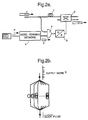
- the packets of data are directed to one or other of two branches of the network. Upstream of the switch 2, part of the signal carried on the network is diverted and gated so that the header of a packet of traffic data is fed to a pulse-coincidence detection gate 3.
- the binary word W forming the address is compared with the complement of a target word T supplied to the gate from a word-forming network 3.
- the input to the word-forming network 3 is provided by a clock-recovery unit CR.
- the output of the gate 3 is converted to an electrical signal by a detector 5 and the resulting signal used to control the switch 2.
- a buffer 1 delays the arrival of the packet at the routing switch 2 until the routing switch has been set correctly.
- the gate 3 carries out a bit-wise Boolean AND operation on the pulse train.
- the gate may consist of a suitable non-linear crystal, oriented in such a way that the two optical pulse trains give rise to efficient generation of second harmonic radiation only if two input pulses A and B are incident simultaneously at the crystal and intersect in the crystal at different angles. This is a technique known as non-collinear SHG (second harmonic generation).
- the crystal orientation satisfies the phase matching condition that ensures no significant SHG occurs with a single pulse on its own.
- the second harmonic output from the crystal is detected and used to control the electro-optic switch 2 to give the correct routing for the packet.
- the routing switch could be, for example, a planar waveguide lithium niobate 2x2 switch with sub-nanosecond switching time, such as is manufactured by E-Tek Dynamics and supplied by Optilas Limited of Milton Keynes.
- the photodetector converts the optical AND signal into an electrical signal.
- An aperture and filter prevent the optical signals input to the crystal from reaching the photodetector, but allow the SHG signal to pass.
- an electronic discriminator may be placed after the photodetector to set a decision threshold level so that the output is one when A and B inputs are present simultaneously.
- Type II phase matching second harmonic generation may be used.
- the two input beams are collinear but their electrical field vectors are polarised in orthogonal directions.
- the crystal is then oriented so that SHG is obtained only when input pulses are present simultaneously in each of two polarisation directions.
- a spectral filter blocks the input beams before they reach the photodetector.
- a clock recovery unit generates an optical clock pulse in exact synchronism with the incoming optical packets (i.e. 1 pulse per packet). This clock recovery may be done using an optical phase locked loop of the type described by S P Dijaili et al [8].
- the clock pulse is then passed through a passive optical network that converts the single pulse into a pulse train that represents a binary word.
- This word-forming network may comprise a multi-wave splitter and recombiner between which are a number of separate optical paths. The lengths of these paths are all slightly different and chosen so that the output pulse train represents the logical complement of the target word T.
- the word-forming network is thus "hard-wired" to produce the required word T.
- This type of passive network may conveniently be fabricated using photolithographic processing together with planar silica waveguide technology (as described for example by C J Beaumont et al [9]).
- the optical delay line shown in the Figure delays the incoming packet until there has been sufficient time for the electro-optic switch to be set correctly.
- the word-forming network may be flexibly configured, for example under network management control. This is of particular use where it is required to change the address of a node or to reconfigure a communications network dynamically, for example in response to a change in traffic demands, or in response to a network fault condition.
- the word-forming network consists of a number of optical paths which can be selected by means of electro-optic or opto-mechanical switches - some or all of the optical paths may contain such a switch. By means of electrical signals applied to these switches, so as to block some paths and unblock or reconfigure others, it is possible to reconfigure the word-forming network in a variety of ways so as in effect to change at will the output word T ⁇ .
- Figure 10 shows a first example of such an approach.
- a number k of fixed word-forming networks are provided, and a given one of the networks is chosen using 1 x k switches.
- Each of the different networks corresponds to a different target word.
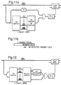
- Figure 11 (a) shows an alternative arrangement where it is possible to perform the word-recognition process on different fields of the header ( Figure 11(b)).
- the word-forming network N (which may be fixed or reconfigurable) is used to recognise whether the input word matches a target word T ⁇ , which in this case is the same length as the sub-divided fields of the header.
- T ⁇ target word
- Figure 12 shows a further alternative embodiment offering even greater flexibility.
- both the target word and also the header field if required can be freely selected by using the switches to configure fully both the target word and the second input to the optical AND gate.
- the word-forming network acts on a datum pulse carried with the word to be recognised, in the manner described in further detail below with respect to Figure 5.
- Configurable word forming networks may also be used similarly with independently generated synchronised pulses in circuit configurations as described, for example, with reference to Figure 2A.
- Figure 5 shows an alternative embodiment which overcomes the need for a locally generated synchronising pulse P in generating the target word.
- the incoming packet is split, with one branch going via a buffer 1 to the routing switch 2 and the other branch being used to provide an input to the AND gate 3.
- the manner in which the other input to the AND gate is generated is modified.
- the incoming packet now includes an additional pulse, the "datum pulse" which precedes the header and has a fixed time relationship to the header pulse train.
- the datum pulse is bit-asynchronous in relation to the header, i.e. it is not separated from the header by an integral number of bit periods. In the presently described example, the datum pulse occurs 1.5 bit periods before the start of the header.
- the incoming packet is split a second time, with one branch being applied to a passive network 4' and the other branch going directly to the input of the optical AND gate 3.
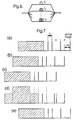
- the network 4' which is shown in further detail in Figure 6, has n arms, where n is the total number of zeros in A.
- the network reproduces and recombines the entire packet including the datum pulse n times, each version being delayed by a time ⁇ j , which is the time difference between the datum pulse and the jth zero in the local address A.
- this has the effect of producing a combined output word T' which has a pulse derived from one of the datum pulses in each bit position of the header where there is a zero in the corresponding bit position of the local address A. There is no pulse in the bit positions where there is a 1 in the local address A.
- the datum pulses are therefore used in effect to generate the binary complement A ⁇ of the local address.
- the output from the network 4' is applied to the AND gate 3 and as before the output from the AND gate 3 is non-zero if H is not equal to A. This technique therefore allows self-routing to occur without the need for bit-level synchronisation at the network node.
- the passive network 4' can be fabricated using compact planar silica-on-silicon technology, providing a component which can readily be exchanged, for example, to allow a change of the local address.
- the bit period is T and the datum pulse occurs 1.5 T before the first bit of the header field H .
- the width of each optical pulse in the packet is substantially shorter than the bit period T .
- the exact amount by which the pulses must be shorter than T depends on factors such as the efficiency of the AND gate, the photo-detector sensitivity, the temporal shape of the pulses, and the optical and electrical noise levels. In practice this should be determined by trial and error; however the following approximate criteria give a guide.
- For rectangular optical pulses of width t we require t ⁇ T /2 .
- t ⁇ T /4 approximately, where t is the full width at half-maximum intensity of the pulse.
- the optical wavelength is 1.55 microns
- the individual optical pulses are 2ps wide.
- the AND gate can have a non-zero output only if the datum pulses that are delayed by the passive network N (and so occur in the signal Figure 5(d) applied to one input of the AND gate) coincide with pulses in the header address field of the non-delayed signal Figure 7(e) which is applied to the other input of the AND gate. This results from the arrangement of the datum pulse so that it is out of synchronism with the rest of the packet, and the use of delays ⁇ j in the passive network N that are non-integer multiples of the bit period T .
- the two splitters are standard fused fibre couplers.
- the splitter ratios are not particularly critical.
- the first splitter could perhaps have a ratio of 10:90% so that most of the energy in the incoming packet is transferred through the routing switch whilst a smaller fraction is passed to the header recognition part of the circuit.
- the second splitter (the one just before the passive network N ) could have a splitting ratio chosen so that the intensities of individual pulses at the two inputs to the optical AND gate are roughly equal.
- the buffer may conveniently be a length of monomode optical fibre - sufficiently long so that the packet is delayed such that the state of the routing switch has been set correctly before the packet arrives at the switch. In this case "sufficient" might be ⁇ 2 ns delay, which would be provided by about 40 cm of fibre.
- the passive device N may conveniently be fabricated using photolithographic processing together with planar silica waveguide technology (as is described for example by CJ Beaumont et al in BT Technology Journal Vol. 9, No 4, Pages 30-35, October 1991).
- the O/E convertor may conveniently be a photomultiplier tube followed by a TTL monostable circuit with an output pulse width just long enough to hold the routing switch in the "activated" state following an electrical output pulse from the photomultiplier tube to allow the complete packet to pass through (for example, a 500 bit packet at 100 Gbit/s would need the switch to be held in the correct state for at least 5 ns).
- the nonlinear optical device used to carry out the optical AND operation may, for example, be a second-harmonic generation crystal, although many other nonlinear optical processes may be used.
- the other components described above are instanced by way of example only. As will be apparent, many alternative device types may be substituted in implementing the invention.
- FIG. 8 One example of an appropriate optical AND gate and detector is shown in Figure 8.
- the system is contained in a lightproof housing 60.
- the lens 61 brings the output from the two input fibres a, b to the same focal spot inside on SHG crystal 62.
- a fraction of the input light is converted to the second harmonic wavelength.
- the crystal is oriented in such a way that a second-harmonic pulse is produced only if a pulse from each of the two fibres is incident simultaneously at the crystal; if a pulse from one of the input fibres reaches the crystal, without simultaneously a pulse from the other fibre, there is no second-harmonic pulse generated.
- This is a well-known technique known as 'non-collinear phase-matching'.
- the purpose of the aperture 63 and filter 64 is to prevent light from the input fibres reaching the photomultiplier, whilst allowing the second-harmonic beam to pass.
- the filter should have a spectral characteristic that attenuates the input wavelength (1.55 ⁇ m) strongly and attenuates the second-harmonic (0.77 ⁇ m) to a much lesser degree.
- a suitable filter would be the glass type KG5 manufactured by Schott Glastechnike.
- the output from the filter passes to a photomultiplier 65.
- Figure 9 shows an alternative AND gate using four-wave mixing in a semiconductor laser amplifier (SLA). This configuration is to be preferred for uses, such as header recognition, which require low latency (i.e. a short response time to incoming signals).
- SLA semiconductor laser amplifier
- two signals (A and B) at wavelength ⁇ s are injected into the SLA in orthogonal polarisation states.
- a CW pump beam P at ⁇ p copolarised with signal A is also injected into the SLA.
- Four-wave mixing occurs between signal A and P to produce primary side-bands at ⁇ s -( ⁇ p - ⁇ s ) and ⁇ p +( ⁇ p - ⁇ s ).
- a gain modulation (and hence refractive index modulation) is impressed on the SLA at the beat frequency between ⁇ p and ⁇ s .
- the signal B sees this modulation and produces side-bands at ⁇ s +( ⁇ p - ⁇ s ) and ⁇ s -( ⁇ p - ⁇ s ) in the orthogonal polarisation state to signals A and P. Mixing does not occur when the pump beam P and signal beam are injected into the SLA orthogonally polarised, so no wavelength conversion of B occurs unless A is also present.
- the signal at ⁇ s -( ⁇ p - ⁇ s ) in the B polarisation plane is isolated through the use of an optical polariser and bandpass filter. This signal represents an AND between signal A and signal B, as the P beam is on continuously.
- signal A at 1553.15nm is combined with a pump P at 1555.08nm from a tunable external cavity laser 91 in a 3dB coupler.
- the combined signal A + P is amplified in an erbium-doped fibre amplifier 92 and passes through a beam splitter/combiner 93 and is combined in an orthogonal polarisation state with A + P.
- the polarisations of A, B and P are optimised for maximum transmission using the fibre pigtailed polarisation beam splitter/combiner.
- the three signals are then coupled into a 500 ⁇ m long strained-layer 8-well MQW buried heterostructure SLA with a gain peak at ⁇ 1.56 ⁇ m when biased at 340mA.
- the output from the SLA passes through a fibre polariser adjusted to extinguish the signals in the A + P polarisation axis. This is followed by a 0.6nm fibre-grating band pass filter centred at 1551.20nm to isolate the AND signal. This signal is further amplified before being detected on a high-speed photodetector (bandwidth ⁇ 18GHz).
- the output from the photodetector may be used, for example, to control a routing switch. For demonstration purposes the output may be viewed on a oscilloscope.
- the circuit of Figure 9 shows the inputs A and B generated using a pulse-pattern generator based on a Mach-Zehnder modulator
- the AND gate may take, for example, the word to be recognised W as input A, and the output of the word-forming network, corresponding to the complement of the target word T ⁇ , as the input B.
- An essential operation in information processing is to recognise binary words (such as, for example, the header address sequences in a packet-switched telecommunications network).
- the present invention uses an alternative approach to word recognition using an algorithm based on AND operations at the bit level. Unlike other logic operations, the AND operation, as represented by the simple scalar product of two optical fields, is fundamental to all ultrafast nonlinear optical phenomena [6].
- the algorithm therefore opens up many new device possibilities having desirable properties such as low latency (short delay time between input and output signals), passive long-term stability, small physical volume and potential for integration.
- the second step is to show that if any other n-bit word were added to the set S q , the property (1) would be rendered invalid.
- W p be an n-bit word containing p ones (p ⁇ q) which is added to S q .
- W p ⁇ W 0 even though W p ⁇ W, so that the condition (1) is made invalid.
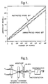
- Figure 1 shows the word length n that is needed, depending on the total number of words required, when using the restricted word set (S n/2 for n even or S (n+1)/2 for n odd) or unrestricted coding (2 n -1).
Landscapes
- Data Exchanges In Wide-Area Networks (AREA)
- Optical Communication System (AREA)
Claims (34)
- Verfahren zum Erkennen eines optisch codierten binären Worts, dadurch gekennzeichnet, daß das Wort erkannt wird, indem im optischen Bereich eine bitweise Boolsche UND-Operation am zu erkennenden Wort W und am Komplement des Zielworts T ausgeführt wird, und daß das codierte Wort aus der Untermenge binärer Wörter gewählt wird, für die



- Verfahren nach Anspruch 1, in dem die UND-Operation dadurch ausgeführt wird, daß ein erstes optisches Signal, das mit dem zu erkennenden Wort W codiert ist, in ein nichtlineares optisches Medium eingeleitet wird, ein zweites optisches Signal, das mit dem Komplement des Zielworts T codiert ist, in das nichtlineare optische Medium eingeleitet wird und der Ausgang des nichtlinearen optischen Mediums erfaßt wird.
- Verfahren nach Anspruch 2, in dem das optische Ausgangssignal des nichtlinearen Mediums vom ersten und vom zweiten optischen Signal kraft seiner Frequenz unterschieden wird.
- Verfahren nach Anspruch 3, in dem das erste und das zweite optische Signal die Frequenz ω besitzen und das optische Ausgangssignal die zweite harmonische Frequenz 2ω besitzt.
- Verfahren nach Anspruch 2, 3 oder 4, in dem das optische Ausgangssignal vom ersten und vom zweiten optischen Signal kraft seiner Ausbreitungsrichtung unterschieden wird.
- Verfahren nach Anspruch 2, 3 oder 4, in dem das optische Ausgangssignal vom ersten und vom zweiten Ausgangssignal kraft seines Polarisationszustands unterschieden wird.
- Verfahren nach Anspruch 2, in dem das optische Ausgangssignal vom ersten und vom zweiten optischen Signal kraft seiner Phase unterschieden wird.
- Verfahren nach irgendeinem der Ansprüche 2 bis 7, in dem das nichtlineare optische Medium ein Kristall ist.
- Verfahren nach irgendeinem der Ansprüche 2 bis 7, in dem das nichtlineare optische Medium ein Lichtwellenleiter ist.
- Verfahren nach irgendeinem der Ansprüche 2 bis 9, das das Einleiten eines optischen Signals in ein wortbildendes Netz enthält, welches so beschaffen ist, daß es einen dem Komplement des Zielworts entsprechenden Ausgang erzeugt.
- Verfahren nach irgendeinem der vorangehenden Ansprüche, in dem die binären Wörter mit einer Bitrate von mehr als 10 GBit/s verarbeitet werden.
- Verfahren nach irgendeinem vorangehenden Anspruch, in dem die Bits w1, w2, .., wn den binären Pixeln eines zu erkennenden Bildes entsprechen.
- Verfahren nach irgendeinem vorangehenden Anspruch, in dem das Codewort W mit einem Datumimpuls versehen ist, der eine feste, bit-asynchrone zeitliche Beziehung zum Rest des Worts besitzt, wobei der Datumimpuls bei der Erzeugung einer Impulsfolge T' in Abhängigkeit vom Zielwort verwendet wird.
- Verfahren nach Anspruch 13, in dem die Impulsfolge T' durch Anwenden des den Datenimpuls enthaltenden Codeworts W auf ein Aufteilungs-/Verzögerungs-Netz erzeugt wird, wobei die verschiedenen Arme des Netzes Verzögerungen besitzen, die in Abhängigkeit vom Zielwort T festgelegt sind.
- Verfahren nach Anspruch 14, in dem jeder j-te Arm des Netzes das Wort W und den entsprechenden Datumimpuls um eine Zeit τj verzögert, die gleich der Zeitdifferenz zwischen dem Datumimpuls und der j-ten Null im Zielwort T ist.
- Verfahren nach irgendeinem der vorangehenden Ansprüche, in dem das Wort W eine Adresse ist, die in einem Kopfsatz eines in einem optischen Netz gesendeten Pakets befördert wird, wobei das Verfahren ferner die Steuerung eines Weiterleitungsschalters für das Paket in Übereinstimmung mit dem Ergebnis der optischen UND-Operation umfaßt.
- Optische Worterkennungsvorrichtung, gekennzeichnet durch ein optisches UND-Gatter und eine Einrichtung zum Eingeben eines zu erkennenden Worts W und des Komplements des Zielworts T in das UND-Gatter und dadurch, daß das optische UND-Gatter so beschaffen ist, daß es das optische Wort durch ein Verfahren nach irgendeinem der vorangehenden Ansprüche erkennt.
- Vorrichtung nach Anspruch 17, die so beschaffen ist, daß sie an ein optisches Nachrichtenübermittlungssystem angeschlossen werden kann, und in der das Wort W eine Adresse ist, die einem im optischen Nachrichtenübermittlungssystem beförderten Paket zugeordnet ist.
- Vorrichtung nach Anspruch 17 oder 18, mit einem nichtlinearen optischen Medium, das als UND-Gatter konfiguriert ist, das Eingänge für erste und zweite optische Signale enthält, und einem Detektor, der so angeschlossen ist, daß er ein Ausgangssignal vom nichtlinearen optischen Medium empfängt.
- Vorrichtung nach Anspruch 19, in dem das nichtlineare optische Medium ein Lichtwellenleiter ist.
- Vorrichtung nach Anspruch 19, in dem das nichtlineare optische Medium ein Kristall ist.
- Vorrichtung nach irgendeinem der Ansprüche 17 bis 21, mit einem wortbildenden Netz (4), das so beschaffen ist, daß es ein Zielwort oder ein daraus abgeleitetes Wort erzeugt.
- Vorrichtung nach Anspruch 22, in der das wortbildende Netz (4) so beschaffen ist, daß es einen dem Komplement des Zielworts entsprechenden Ausgang erzeugt.
- Vorrichtung nach irgendeinem der Ansprüche 17 bis 23, gekennzeichnet durch einen optischen Impulsfolgengenerator (4'), der auf einen mit dem Codewort W transportierten Datumimpuls anspricht, der zum Rest des Codeworts eine feste, bit-asynchrone zeitliche Beziehung besitzt, wobei der Impulsfolgengenerator eine vom Zielwort T abhängende Impulsfolge T' ausgibt.
- Optisches Nachrichtenübermittlungssystem, in dem optische Pakete n-Bit-Identifiziererwörter W befördern, dadurch gekennzeichnet, daß die Identifiziererwörter W aus der Untermenge binärer Wörter gewählt sind, für die für irgendwelche zwei Wörter W und T aus der Untermenge


- Verfahren zum Codieren eines Signals für die Übertragung im optischen Bereich, dadurch gekennzeichnet, daß das Signal mit einem binären Wort codiert wird, das aus einer Untermenge von binären Wörtern gewählt ist, für die für irgendwelche zwei Wörter W und T aus der Untermenge


- Verfahren nach Anspruch 26, das ferner die Erzeugung eines Datumimpulses enthält, der mit dem Rest des Codeworts W in einer festen, bit-asynchronen zeitlichen Beziehung steht.
- Optisches Nachrichtenübermittlungssystem, gekennzeichnet durch eine Einrichtung zum Erkennen eines optischen Codeworts durch Anwenden des zu erkennenden optischen Codeworts W auf eine optische Impulsfolge, wobei


- Verfahren nach Anspruch 10 oder irgendeinem der Ansprüche 11 bis 16 in Verbindung mit Anspruch 10, in dem das wortbildende Netz eine optische Schalteinrichtung besitzt und durch die optische Schalteinrichtung so konfiguriert ist, daß ein ausgewähltes Wort aus mehreren verschiedenen Zielwörtern erkannt wird.
- Verfahren nach Anspruch 10 oder irgendeinem der Ansprüche 11 bis 16 in Verbindung mit Anspruch 10 oder nach Anspruch 29, das ferner das Auswählen eines von mehreren Unterfeldern einer ankommenden Impulsfolge als das zu erkennende Wort W umfaßt.
- Vorrichtung zum Erkennen eines optisch codierten binären Worts, gekennzeichnet durch ein optisches UND-Gatter mit einem ersten optischen Eingang für ein zu erkennendes Wort W und einem zweiten optischen Eingang für das Komplement eines Zielworts T, und einen Detektor, der auf den Ausgang des UND-Gatters anspricht, wobei das UND-Gatter so beschaffen ist, daß es im optischen Gebiet eine bitweise Boolsche UND-Operation an den eingegebenen Wörtern ausführt.
- Vorrichtung nach Anspruch 31, mit einem wortbildenden Netz, das so beschaffen ist, daß es ein Zielwort oder ein aus dem Zielwort abgeleitetes Wort erzeugt, um es in das optische UND-Gatter einzugeben.
- Vorrichtung nach Anspruch 32, in dem das wortbildende Netz eine optische Schalteinrichtung enthält und durch die optische Schalteinrichtung so konfiguriert ist, daß es ein ausgewähltes Wort mehrerer verschiedener Zielwörter erkennt.
- Vorrichtung nach Anspruch 32 oder 33, mit einer Einrichtung zum Auswählen eines von mehreren Unterfeldern einer ankommenden Impulsfolge als das zu erkennende Wort W.
Priority Applications (1)
| Application Number | Priority Date | Filing Date | Title |
|---|---|---|---|
| EP94907651A EP0687370B1 (de) | 1993-03-02 | 1994-03-01 | Verfahren und vorrichtung zur erkennung von optisch kodierten signalen |
Applications Claiming Priority (6)
| Application Number | Priority Date | Filing Date | Title |
|---|---|---|---|
| EP93301568 | 1993-03-02 | ||
| EP93301568 | 1993-03-02 | ||
| GB9318799 | 1993-09-10 | ||
| GB939318799A GB9318799D0 (en) | 1993-09-10 | 1993-09-10 | Optical codeword recognition |
| PCT/GB1994/000397 WO1994021088A2 (en) | 1993-03-02 | 1994-03-01 | Optically encoded signals |
| EP94907651A EP0687370B1 (de) | 1993-03-02 | 1994-03-01 | Verfahren und vorrichtung zur erkennung von optisch kodierten signalen |
Publications (2)
| Publication Number | Publication Date |
|---|---|
| EP0687370A1 EP0687370A1 (de) | 1995-12-20 |
| EP0687370B1 true EP0687370B1 (de) | 1997-07-09 |
Family
ID=27235383
Family Applications (1)
| Application Number | Title | Priority Date | Filing Date |
|---|---|---|---|
| EP94907651A Expired - Lifetime EP0687370B1 (de) | 1993-03-02 | 1994-03-01 | Verfahren und vorrichtung zur erkennung von optisch kodierten signalen |
Country Status (1)
| Country | Link |
|---|---|
| EP (1) | EP0687370B1 (de) |
Families Citing this family (1)
| Publication number | Priority date | Publication date | Assignee | Title |
|---|---|---|---|---|
| DE60038016T2 (de) | 1999-05-11 | 2009-02-12 | British Telecommunications P.L.C. | Optisches kommunikationsnetzwerk |
-
1994
- 1994-03-01 EP EP94907651A patent/EP0687370B1/de not_active Expired - Lifetime
Non-Patent Citations (1)
| Title |
|---|
| Optische Computer, Fumio Inaba, Springer-Verlag Berlin 1992, pages 76 - 84 * |
Also Published As
| Publication number | Publication date |
|---|---|
| EP0687370A1 (de) | 1995-12-20 |
Similar Documents
| Publication | Publication Date | Title |
|---|---|---|
| CA2157492C (en) | Optically encoded signals | |
| US4866699A (en) | Optical telecommunications system using code division multiple access | |
| US5880866A (en) | Time division demultiplexing using selective Raman amplification | |
| Cardakli et al. | Reconfigurable optical packet header recognition and routing using time-to-wavelength mapping and tunable fiber Bragg gratings for correlation decoding | |
| US6151428A (en) | All-optical wavelength coded logic gates | |
| Prucnal et al. | Demonstration of a rapidly tunable optical time-division multiple-access coder | |
| US5760948A (en) | Method of regenerating a soliton signal using an all optical doubler | |
| Vahala et al. | Ultrafast WDM logic | |
| Martinez et al. | All optical N-bit XOR gate with feedback for optical packet header processing | |
| Sauer et al. | A soliton ring network | |
| Liu et al. | Photonic firewall oriented fast all-optical binary pattern recognition | |
| EP0687370A1 (de) | Verfahren zur erkennung von optisch kodierten signalen | |
| HK1001009B (en) | Method of and device for recognizing optically encoded signals | |
| Bergman et al. | Advances in multichannel multiGbytes/s bit-parallel WDM single fiber link | |
| Li et al. | Power equalization for SOA-based dual-loop optical buffer by optical control pulse optimization | |
| JPH07131441A (ja) | 光多重分離装置 | |
| JP2827501B2 (ja) | 光セルフ・ルーテイング回路 | |
| US6542269B1 (en) | Optical device for processing an optical impulse | |
| Naciri et al. | Acousto‐optic deflector‐based optical packet synchronization | |
| Cinato et al. | Photonics applications in switching: an ATM optical node | |
| Sokoloff et al. | Efficiently packaged ultrafast demultiplexers for high bandwidth optical TDM systems | |
| Blumenthal et al. | Self-routing of 12.5-Gbit/s data through an 8× 8 LiNbO3 optical crossbar switch matrix with gigahertz switching speed | |
| Shin et al. | 10 Gb/s optical packet header recognition using a new fiber-optic matched filter | |
| Mosso et al. | OTDM quasi-all-optical demultiplexing techniques comparative analysis | |
| Verber et al. | Progress toward the development of a 100 Gb/s optical data link |
Legal Events
| Date | Code | Title | Description |
|---|---|---|---|
| PUAI | Public reference made under article 153(3) epc to a published international application that has entered the european phase |
Free format text: ORIGINAL CODE: 0009012 |
|
| 17P | Request for examination filed |
Effective date: 19950830 |
|
| AK | Designated contracting states |
Kind code of ref document: A1 Designated state(s): BE CH DE ES FR GB IE IT LI NL SE |
|
| 17Q | First examination report despatched |
Effective date: 19951218 |
|
| GRAG | Despatch of communication of intention to grant |
Free format text: ORIGINAL CODE: EPIDOS AGRA |
|
| GRAH | Despatch of communication of intention to grant a patent |
Free format text: ORIGINAL CODE: EPIDOS IGRA |
|
| GRAH | Despatch of communication of intention to grant a patent |
Free format text: ORIGINAL CODE: EPIDOS IGRA |
|
| GRAA | (expected) grant |
Free format text: ORIGINAL CODE: 0009210 |
|
| AK | Designated contracting states |
Kind code of ref document: B1 Designated state(s): BE CH DE ES FR GB IE IT LI NL SE |
|
| REG | Reference to a national code |
Ref country code: CH Ref legal event code: EP |
|
| REF | Corresponds to: |
Ref document number: 69404130 Country of ref document: DE Date of ref document: 19970814 |
|
| REG | Reference to a national code |
Ref country code: ES Ref legal event code: FG2A Ref document number: 2105652 Country of ref document: ES Kind code of ref document: T3 |
|
| ET | Fr: translation filed | ||
| REG | Reference to a national code |
Ref country code: CH Ref legal event code: NV Representative=s name: JACOBACCI & PERANI S.A. |
|
| PG25 | Lapsed in a contracting state [announced via postgrant information from national office to epo] |
Ref country code: IE Free format text: LAPSE BECAUSE OF NON-PAYMENT OF DUE FEES Effective date: 19980301 |
|
| PLBE | No opposition filed within time limit |
Free format text: ORIGINAL CODE: 0009261 |
|
| STAA | Information on the status of an ep patent application or granted ep patent |
Free format text: STATUS: NO OPPOSITION FILED WITHIN TIME LIMIT |
|
| 26N | No opposition filed | ||
| REG | Reference to a national code |
Ref country code: GB Ref legal event code: 732E |
|
| REG | Reference to a national code |
Ref country code: GB Ref legal event code: IF02 |
|
| PGFP | Annual fee paid to national office [announced via postgrant information from national office to epo] |
Ref country code: CH Payment date: 20020214 Year of fee payment: 9 |
|
| PGFP | Annual fee paid to national office [announced via postgrant information from national office to epo] |
Ref country code: NL Payment date: 20020225 Year of fee payment: 9 |
|
| PGFP | Annual fee paid to national office [announced via postgrant information from national office to epo] |
Ref country code: ES Payment date: 20020308 Year of fee payment: 9 |
|
| PG25 | Lapsed in a contracting state [announced via postgrant information from national office to epo] |
Ref country code: ES Free format text: LAPSE BECAUSE OF NON-PAYMENT OF DUE FEES Effective date: 20030303 |
|
| PG25 | Lapsed in a contracting state [announced via postgrant information from national office to epo] |
Ref country code: LI Free format text: LAPSE BECAUSE OF NON-PAYMENT OF DUE FEES Effective date: 20030331 Ref country code: CH Free format text: LAPSE BECAUSE OF NON-PAYMENT OF DUE FEES Effective date: 20030331 |
|
| PG25 | Lapsed in a contracting state [announced via postgrant information from national office to epo] |
Ref country code: NL Free format text: LAPSE BECAUSE OF NON-PAYMENT OF DUE FEES Effective date: 20031001 |
|
| REG | Reference to a national code |
Ref country code: CH Ref legal event code: PL |
|
| NLV4 | Nl: lapsed or anulled due to non-payment of the annual fee |
Effective date: 20031001 |
|
| REG | Reference to a national code |
Ref country code: ES Ref legal event code: FD2A Effective date: 20030303 |
|
| PGFP | Annual fee paid to national office [announced via postgrant information from national office to epo] |
Ref country code: SE Payment date: 20080218 Year of fee payment: 15 Ref country code: IT Payment date: 20080216 Year of fee payment: 15 Ref country code: GB Payment date: 20080228 Year of fee payment: 15 |
|
| PGFP | Annual fee paid to national office [announced via postgrant information from national office to epo] |
Ref country code: FR Payment date: 20080211 Year of fee payment: 15 Ref country code: DE Payment date: 20080227 Year of fee payment: 15 |
|
| PGFP | Annual fee paid to national office [announced via postgrant information from national office to epo] |
Ref country code: BE Payment date: 20080313 Year of fee payment: 15 |
|
| BERE | Be: lapsed |
Owner name: BRITISH *TELECOMMUNICATIONS P.L.C. Effective date: 20090331 |
|
| EUG | Se: european patent has lapsed | ||
| GBPC | Gb: european patent ceased through non-payment of renewal fee |
Effective date: 20090301 |
|
| REG | Reference to a national code |
Ref country code: FR Ref legal event code: ST Effective date: 20091130 |
|
| PG25 | Lapsed in a contracting state [announced via postgrant information from national office to epo] |
Ref country code: DE Free format text: LAPSE BECAUSE OF NON-PAYMENT OF DUE FEES Effective date: 20091001 |
|
| PG25 | Lapsed in a contracting state [announced via postgrant information from national office to epo] |
Ref country code: BE Free format text: LAPSE BECAUSE OF NON-PAYMENT OF DUE FEES Effective date: 20090331 |
|
| PG25 | Lapsed in a contracting state [announced via postgrant information from national office to epo] |
Ref country code: GB Free format text: LAPSE BECAUSE OF NON-PAYMENT OF DUE FEES Effective date: 20090301 Ref country code: FR Free format text: LAPSE BECAUSE OF NON-PAYMENT OF DUE FEES Effective date: 20091123 |
|
| PG25 | Lapsed in a contracting state [announced via postgrant information from national office to epo] |
Ref country code: IT Free format text: LAPSE BECAUSE OF NON-PAYMENT OF DUE FEES Effective date: 20090301 |
|
| PG25 | Lapsed in a contracting state [announced via postgrant information from national office to epo] |
Ref country code: SE Free format text: LAPSE BECAUSE OF NON-PAYMENT OF DUE FEES Effective date: 20090302 |