EP0687925A2 - Methode zur Herstellung eines optischen Einkoppelwellenleiters und Lichtleiteranordnung mit dem Einkoppelwellenleiter - Google Patents
Methode zur Herstellung eines optischen Einkoppelwellenleiters und Lichtleiteranordnung mit dem Einkoppelwellenleiter Download PDFInfo
- Publication number
- EP0687925A2 EP0687925A2 EP95108052A EP95108052A EP0687925A2 EP 0687925 A2 EP0687925 A2 EP 0687925A2 EP 95108052 A EP95108052 A EP 95108052A EP 95108052 A EP95108052 A EP 95108052A EP 0687925 A2 EP0687925 A2 EP 0687925A2
- Authority
- EP
- European Patent Office
- Prior art keywords
- optical coupling
- lightguide
- coupling waveguide
- polymeric optical
- layer
- Prior art date
- Legal status (The legal status is an assumption and is not a legal conclusion. Google has not performed a legal analysis and makes no representation as to the accuracy of the status listed.)
- Withdrawn
Links
- 230000003287 optical effect Effects 0.000 title claims abstract description 128
- 230000008878 coupling Effects 0.000 title claims abstract description 113
- 238000010168 coupling process Methods 0.000 title claims abstract description 113
- 238000005859 coupling reaction Methods 0.000 title claims abstract description 113
- 238000000034 method Methods 0.000 title claims abstract description 51
- 229920000642 polymer Polymers 0.000 claims abstract description 46
- 239000000203 mixture Substances 0.000 claims abstract description 17
- 239000000178 monomer Substances 0.000 claims abstract description 10
- 238000000059 patterning Methods 0.000 claims abstract description 4
- 230000003381 solubilizing effect Effects 0.000 claims abstract description 3
- 238000005253 cladding Methods 0.000 claims description 37
- 230000007423 decrease Effects 0.000 claims description 8
- 229920001577 copolymer Polymers 0.000 claims description 4
- 238000000206 photolithography Methods 0.000 claims description 2
- 239000002904 solvent Substances 0.000 abstract description 9
- 239000010410 layer Substances 0.000 description 57
- -1 n-stearyl acrylate Chemical compound 0.000 description 33
- 239000000463 material Substances 0.000 description 19
- XEKOWRVHYACXOJ-UHFFFAOYSA-N Ethyl acetate Chemical compound CCOC(C)=O XEKOWRVHYACXOJ-UHFFFAOYSA-N 0.000 description 12
- OKKJLVBELUTLKV-UHFFFAOYSA-N Methanol Chemical compound OC OKKJLVBELUTLKV-UHFFFAOYSA-N 0.000 description 12
- 239000000243 solution Substances 0.000 description 12
- JHIVVAPYMSGYDF-UHFFFAOYSA-N cyclohexanone Chemical compound O=C1CCCCC1 JHIVVAPYMSGYDF-UHFFFAOYSA-N 0.000 description 10
- 239000011521 glass Substances 0.000 description 9
- 229920003229 poly(methyl methacrylate) Polymers 0.000 description 9
- 239000004926 polymethyl methacrylate Substances 0.000 description 9
- 239000004065 semiconductor Substances 0.000 description 9
- 239000000758 substrate Substances 0.000 description 9
- 229910001218 Gallium arsenide Inorganic materials 0.000 description 8
- 239000007788 liquid Substances 0.000 description 8
- 239000013307 optical fiber Substances 0.000 description 7
- WEVYAHXRMPXWCK-UHFFFAOYSA-N Acetonitrile Chemical compound CC#N WEVYAHXRMPXWCK-UHFFFAOYSA-N 0.000 description 6
- WYURNTSHIVDZCO-UHFFFAOYSA-N Tetrahydrofuran Chemical compound C1CCOC1 WYURNTSHIVDZCO-UHFFFAOYSA-N 0.000 description 6
- YXFVVABEGXRONW-UHFFFAOYSA-N Toluene Chemical compound CC1=CC=CC=C1 YXFVVABEGXRONW-UHFFFAOYSA-N 0.000 description 6
- 239000003795 chemical substances by application Substances 0.000 description 6
- 238000005516 engineering process Methods 0.000 description 6
- VVQNEPGJFQJSBK-UHFFFAOYSA-N Methyl methacrylate Chemical compound COC(=O)C(C)=C VVQNEPGJFQJSBK-UHFFFAOYSA-N 0.000 description 5
- 150000001875 compounds Chemical class 0.000 description 5
- 239000010432 diamond Substances 0.000 description 5
- 229910003460 diamond Inorganic materials 0.000 description 5
- 238000006073 displacement reaction Methods 0.000 description 5
- 229910052724 xenon Inorganic materials 0.000 description 5
- FHNFHKCVQCLJFQ-UHFFFAOYSA-N xenon atom Chemical compound [Xe] FHNFHKCVQCLJFQ-UHFFFAOYSA-N 0.000 description 5
- 229910003327 LiNbO3 Inorganic materials 0.000 description 4
- 239000004793 Polystyrene Substances 0.000 description 4
- 238000001723 curing Methods 0.000 description 4
- 239000000975 dye Substances 0.000 description 4
- 238000004519 manufacturing process Methods 0.000 description 4
- 229920002223 polystyrene Polymers 0.000 description 4
- 238000002360 preparation method Methods 0.000 description 4
- 239000002002 slurry Substances 0.000 description 4
- CSCPPACGZOOCGX-UHFFFAOYSA-N Acetone Chemical compound CC(C)=O CSCPPACGZOOCGX-UHFFFAOYSA-N 0.000 description 3
- 239000004952 Polyamide Substances 0.000 description 3
- 239000004642 Polyimide Substances 0.000 description 3
- 239000000853 adhesive Substances 0.000 description 3
- 230000001070 adhesive effect Effects 0.000 description 3
- 238000006243 chemical reaction Methods 0.000 description 3
- 239000013256 coordination polymer Substances 0.000 description 3
- 230000000694 effects Effects 0.000 description 3
- 239000000835 fiber Substances 0.000 description 3
- 230000010354 integration Effects 0.000 description 3
- 229920002120 photoresistant polymer Polymers 0.000 description 3
- 238000001020 plasma etching Methods 0.000 description 3
- 229920002647 polyamide Polymers 0.000 description 3
- 239000004417 polycarbonate Substances 0.000 description 3
- 229920000515 polycarbonate Polymers 0.000 description 3
- 229920001721 polyimide Polymers 0.000 description 3
- 238000004528 spin coating Methods 0.000 description 3
- YLQBMQCUIZJEEH-UHFFFAOYSA-N tetrahydrofuran Natural products C=1C=COC=1 YLQBMQCUIZJEEH-UHFFFAOYSA-N 0.000 description 3
- WBYWAXJHAXSJNI-VOTSOKGWSA-M .beta-Phenylacrylic acid Natural products [O-]C(=O)\C=C\C1=CC=CC=C1 WBYWAXJHAXSJNI-VOTSOKGWSA-M 0.000 description 2
- OZAIFHULBGXAKX-UHFFFAOYSA-N 2-(2-cyanopropan-2-yldiazenyl)-2-methylpropanenitrile Chemical compound N#CC(C)(C)N=NC(C)(C)C#N OZAIFHULBGXAKX-UHFFFAOYSA-N 0.000 description 2
- VVBLNCFGVYUYGU-UHFFFAOYSA-N 4,4'-Bis(dimethylamino)benzophenone Chemical compound C1=CC(N(C)C)=CC=C1C(=O)C1=CC=C(N(C)C)C=C1 VVBLNCFGVYUYGU-UHFFFAOYSA-N 0.000 description 2
- WBYWAXJHAXSJNI-SREVYHEPSA-N Cinnamic acid Chemical compound OC(=O)\C=C/C1=CC=CC=C1 WBYWAXJHAXSJNI-SREVYHEPSA-N 0.000 description 2
- XDTMQSROBMDMFD-UHFFFAOYSA-N Cyclohexane Chemical compound C1CCCCC1 XDTMQSROBMDMFD-UHFFFAOYSA-N 0.000 description 2
- SECXISVLQFMRJM-UHFFFAOYSA-N N-Methylpyrrolidone Chemical compound CN1CCCC1=O SECXISVLQFMRJM-UHFFFAOYSA-N 0.000 description 2
- XUIMIQQOPSSXEZ-UHFFFAOYSA-N Silicon Chemical compound [Si] XUIMIQQOPSSXEZ-UHFFFAOYSA-N 0.000 description 2
- UIIMBOGNXHQVGW-UHFFFAOYSA-M Sodium bicarbonate Chemical compound [Na+].OC([O-])=O UIIMBOGNXHQVGW-UHFFFAOYSA-M 0.000 description 2
- PPBRXRYQALVLMV-UHFFFAOYSA-N Styrene Chemical compound C=CC1=CC=CC=C1 PPBRXRYQALVLMV-UHFFFAOYSA-N 0.000 description 2
- GWEVSGVZZGPLCZ-UHFFFAOYSA-N Titan oxide Chemical compound O=[Ti]=O GWEVSGVZZGPLCZ-UHFFFAOYSA-N 0.000 description 2
- 229910052799 carbon Inorganic materials 0.000 description 2
- 229930016911 cinnamic acid Natural products 0.000 description 2
- 235000013985 cinnamic acid Nutrition 0.000 description 2
- 239000011248 coating agent Substances 0.000 description 2
- 238000000576 coating method Methods 0.000 description 2
- 239000003431 cross linking reagent Substances 0.000 description 2
- RWGFKTVRMDUZSP-UHFFFAOYSA-N cumene Chemical compound CC(C)C1=CC=CC=C1 RWGFKTVRMDUZSP-UHFFFAOYSA-N 0.000 description 2
- 230000003247 decreasing effect Effects 0.000 description 2
- 238000005530 etching Methods 0.000 description 2
- 230000006872 improvement Effects 0.000 description 2
- 239000003999 initiator Substances 0.000 description 2
- 229910001410 inorganic ion Inorganic materials 0.000 description 2
- PSGAAPLEWMOORI-PEINSRQWSA-N medroxyprogesterone acetate Chemical compound C([C@@]12C)CC(=O)C=C1[C@@H](C)C[C@@H]1[C@@H]2CC[C@]2(C)[C@@](OC(C)=O)(C(C)=O)CC[C@H]21 PSGAAPLEWMOORI-PEINSRQWSA-N 0.000 description 2
- WBYWAXJHAXSJNI-UHFFFAOYSA-N methyl p-hydroxycinnamate Natural products OC(=O)C=CC1=CC=CC=C1 WBYWAXJHAXSJNI-UHFFFAOYSA-N 0.000 description 2
- ZKATWMILCYLAPD-UHFFFAOYSA-N niobium pentoxide Chemical compound O=[Nb](=O)O[Nb](=O)=O ZKATWMILCYLAPD-UHFFFAOYSA-N 0.000 description 2
- 229920002635 polyurethane Polymers 0.000 description 2
- 239000004814 polyurethane Substances 0.000 description 2
- 230000008569 process Effects 0.000 description 2
- 229910052710 silicon Inorganic materials 0.000 description 2
- 239000010703 silicon Substances 0.000 description 2
- 239000005361 soda-lime glass Substances 0.000 description 2
- XHAFIUUYXQFJEW-UHFFFAOYSA-N 1-chloroethenylbenzene Chemical compound ClC(=C)C1=CC=CC=C1 XHAFIUUYXQFJEW-UHFFFAOYSA-N 0.000 description 1
- KWVGIHKZDCUPEU-UHFFFAOYSA-N 2,2-dimethoxy-2-phenylacetophenone Chemical compound C=1C=CC=CC=1C(OC)(OC)C(=O)C1=CC=CC=C1 KWVGIHKZDCUPEU-UHFFFAOYSA-N 0.000 description 1
- SMZOUWXMTYCWNB-UHFFFAOYSA-N 2-(2-methoxy-5-methylphenyl)ethanamine Chemical compound COC1=CC=C(C)C=C1CCN SMZOUWXMTYCWNB-UHFFFAOYSA-N 0.000 description 1
- GOXQRTZXKQZDDN-UHFFFAOYSA-N 2-Ethylhexyl acrylate Chemical compound CCCCC(CC)COC(=O)C=C GOXQRTZXKQZDDN-UHFFFAOYSA-N 0.000 description 1
- NIXOWILDQLNWCW-UHFFFAOYSA-N 2-Propenoic acid Natural products OC(=O)C=C NIXOWILDQLNWCW-UHFFFAOYSA-N 0.000 description 1
- FOQABOMYTOFLPZ-UHFFFAOYSA-N 2-[n-ethyl-4-[(4-nitrophenyl)diazenyl]anilino]ethanol Chemical compound C1=CC(N(CCO)CC)=CC=C1N=NC1=CC=C([N+]([O-])=O)C=C1 FOQABOMYTOFLPZ-UHFFFAOYSA-N 0.000 description 1
- FWWXYLGCHHIKNY-UHFFFAOYSA-N 2-ethoxyethyl prop-2-enoate Chemical compound CCOCCOC(=O)C=C FWWXYLGCHHIKNY-UHFFFAOYSA-N 0.000 description 1
- OMIGHNLMNHATMP-UHFFFAOYSA-N 2-hydroxyethyl prop-2-enoate Chemical compound OCCOC(=O)C=C OMIGHNLMNHATMP-UHFFFAOYSA-N 0.000 description 1
- GWZMWHWAWHPNHN-UHFFFAOYSA-N 2-hydroxypropyl prop-2-enoate Chemical compound CC(O)COC(=O)C=C GWZMWHWAWHPNHN-UHFFFAOYSA-N 0.000 description 1
- HFCUBKYHMMPGBY-UHFFFAOYSA-N 2-methoxyethyl prop-2-enoate Chemical compound COCCOC(=O)C=C HFCUBKYHMMPGBY-UHFFFAOYSA-N 0.000 description 1
- QTWJRLJHJPIABL-UHFFFAOYSA-N 2-methylphenol;3-methylphenol;4-methylphenol Chemical compound CC1=CC=C(O)C=C1.CC1=CC=CC(O)=C1.CC1=CC=CC=C1O QTWJRLJHJPIABL-UHFFFAOYSA-N 0.000 description 1
- KGIGUEBEKRSTEW-UHFFFAOYSA-N 2-vinylpyridine Chemical compound C=CC1=CC=CC=N1 KGIGUEBEKRSTEW-UHFFFAOYSA-N 0.000 description 1
- OZAIFHULBGXAKX-VAWYXSNFSA-N AIBN Substances N#CC(C)(C)\N=N\C(C)(C)C#N OZAIFHULBGXAKX-VAWYXSNFSA-N 0.000 description 1
- IJGRMHOSHXDMSA-UHFFFAOYSA-N Atomic nitrogen Chemical compound N#N IJGRMHOSHXDMSA-UHFFFAOYSA-N 0.000 description 1
- 239000004698 Polyethylene Substances 0.000 description 1
- VYPSYNLAJGMNEJ-UHFFFAOYSA-N Silicium dioxide Chemical compound O=[Si]=O VYPSYNLAJGMNEJ-UHFFFAOYSA-N 0.000 description 1
- 150000001252 acrylic acid derivatives Chemical class 0.000 description 1
- 125000003647 acryloyl group Chemical group O=C([*])C([H])=C([H])[H] 0.000 description 1
- 150000001408 amides Chemical class 0.000 description 1
- 239000012298 atmosphere Substances 0.000 description 1
- 239000006121 base glass Substances 0.000 description 1
- 230000008901 benefit Effects 0.000 description 1
- 230000015572 biosynthetic process Effects 0.000 description 1
- DKVNPHBNOWQYFE-UHFFFAOYSA-N carbamodithioic acid Chemical group NC(S)=S DKVNPHBNOWQYFE-UHFFFAOYSA-N 0.000 description 1
- 239000003054 catalyst Substances 0.000 description 1
- 239000012792 core layer Substances 0.000 description 1
- 229930003836 cresol Natural products 0.000 description 1
- KBLWLMPSVYBVDK-UHFFFAOYSA-N cyclohexyl prop-2-enoate Chemical compound C=CC(=O)OC1CCCCC1 KBLWLMPSVYBVDK-UHFFFAOYSA-N 0.000 description 1
- 125000000664 diazo group Chemical group [N-]=[N+]=[*] 0.000 description 1
- 239000003989 dielectric material Substances 0.000 description 1
- 229910001873 dinitrogen Inorganic materials 0.000 description 1
- 238000001035 drying Methods 0.000 description 1
- SUPCQIBBMFXVTL-UHFFFAOYSA-N ethyl 2-methylprop-2-enoate Chemical compound CCOC(=O)C(C)=C SUPCQIBBMFXVTL-UHFFFAOYSA-N 0.000 description 1
- XWNVSPGTJSGNPU-UHFFFAOYSA-N ethyl 4-chloro-1h-indole-2-carboxylate Chemical compound C1=CC=C2NC(C(=O)OCC)=CC2=C1Cl XWNVSPGTJSGNPU-UHFFFAOYSA-N 0.000 description 1
- 238000001704 evaporation Methods 0.000 description 1
- 125000001153 fluoro group Chemical group F* 0.000 description 1
- 125000000524 functional group Chemical group 0.000 description 1
- 239000005350 fused silica glass Substances 0.000 description 1
- VOZRXNHHFUQHIL-UHFFFAOYSA-N glycidyl methacrylate Chemical compound CC(=C)C(=O)OCC1CO1 VOZRXNHHFUQHIL-UHFFFAOYSA-N 0.000 description 1
- 125000004435 hydrogen atom Chemical group [H]* 0.000 description 1
- 150000002734 metacrylic acid derivatives Chemical class 0.000 description 1
- 239000011259 mixed solution Substances 0.000 description 1
- 238000002156 mixing Methods 0.000 description 1
- QVEIBLDXZNGPHR-UHFFFAOYSA-N naphthalene-1,4-dione;diazide Chemical compound [N-]=[N+]=[N-].[N-]=[N+]=[N-].C1=CC=C2C(=O)C=CC(=O)C2=C1 QVEIBLDXZNGPHR-UHFFFAOYSA-N 0.000 description 1
- 229910052757 nitrogen Inorganic materials 0.000 description 1
- 229920003986 novolac Polymers 0.000 description 1
- 150000002924 oxiranes Chemical class 0.000 description 1
- 229920001568 phenolic resin Polymers 0.000 description 1
- 239000005011 phenolic resin Substances 0.000 description 1
- 238000000016 photochemical curing Methods 0.000 description 1
- 238000005498 polishing Methods 0.000 description 1
- 229920003227 poly(N-vinyl carbazole) Polymers 0.000 description 1
- 229920005593 poly(benzyl methacrylate) Polymers 0.000 description 1
- 229920002776 polycyclohexyl methacrylate Polymers 0.000 description 1
- 229920000573 polyethylene Polymers 0.000 description 1
- 239000002861 polymer material Substances 0.000 description 1
- 229920000193 polymethacrylate Polymers 0.000 description 1
- 229920000182 polyphenyl methacrylate Polymers 0.000 description 1
- 229920001343 polytetrafluoroethylene Polymers 0.000 description 1
- 229920000915 polyvinyl chloride Polymers 0.000 description 1
- 239000004800 polyvinyl chloride Substances 0.000 description 1
- 238000001556 precipitation Methods 0.000 description 1
- HJWLCRVIBGQPNF-UHFFFAOYSA-N prop-2-enylbenzene Chemical compound C=CCC1=CC=CC=C1 HJWLCRVIBGQPNF-UHFFFAOYSA-N 0.000 description 1
- 230000001902 propagating effect Effects 0.000 description 1
- BOQSSGDQNWEFSX-UHFFFAOYSA-N propan-2-yl 2-methylprop-2-enoate Chemical compound CC(C)OC(=O)C(C)=C BOQSSGDQNWEFSX-UHFFFAOYSA-N 0.000 description 1
- NHARPDSAXCBDDR-UHFFFAOYSA-N propyl 2-methylprop-2-enoate Chemical compound CCCOC(=O)C(C)=C NHARPDSAXCBDDR-UHFFFAOYSA-N 0.000 description 1
- 230000009467 reduction Effects 0.000 description 1
- 239000012047 saturated solution Substances 0.000 description 1
- 229910000030 sodium bicarbonate Inorganic materials 0.000 description 1
- 235000017557 sodium bicarbonate Nutrition 0.000 description 1
- 239000007787 solid Substances 0.000 description 1
- 239000000126 substance Substances 0.000 description 1
- PBCFLUZVCVVTBY-UHFFFAOYSA-N tantalum pentoxide Inorganic materials O=[Ta](=O)O[Ta](=O)=O PBCFLUZVCVVTBY-UHFFFAOYSA-N 0.000 description 1
- 125000000391 vinyl group Chemical group [H]C([*])=C([H])[H] 0.000 description 1
- 229920002554 vinyl polymer Polymers 0.000 description 1
- XLYOFNOQVPJJNP-UHFFFAOYSA-N water Substances O XLYOFNOQVPJJNP-UHFFFAOYSA-N 0.000 description 1
- 238000009736 wetting Methods 0.000 description 1
Images

Classifications
-
- G—PHYSICS
- G02—OPTICS
- G02B—OPTICAL ELEMENTS, SYSTEMS OR APPARATUS
- G02B6/00—Light guides; Structural details of arrangements comprising light guides and other optical elements, e.g. couplings
- G02B6/10—Light guides; Structural details of arrangements comprising light guides and other optical elements, e.g. couplings of the optical waveguide type
- G02B6/12—Light guides; Structural details of arrangements comprising light guides and other optical elements, e.g. couplings of the optical waveguide type of the integrated circuit kind
- G02B6/122—Basic optical elements, e.g. light-guiding paths
- G02B6/1221—Basic optical elements, e.g. light-guiding paths made from organic materials
-
- G—PHYSICS
- G02—OPTICS
- G02B—OPTICAL ELEMENTS, SYSTEMS OR APPARATUS
- G02B6/00—Light guides; Structural details of arrangements comprising light guides and other optical elements, e.g. couplings
- G02B6/10—Light guides; Structural details of arrangements comprising light guides and other optical elements, e.g. couplings of the optical waveguide type
- G02B6/12—Light guides; Structural details of arrangements comprising light guides and other optical elements, e.g. couplings of the optical waveguide type of the integrated circuit kind
- G02B6/122—Basic optical elements, e.g. light-guiding paths
- G02B6/1228—Tapered waveguides, e.g. integrated spot-size transformers
-
- G—PHYSICS
- G02—OPTICS
- G02B—OPTICAL ELEMENTS, SYSTEMS OR APPARATUS
- G02B6/00—Light guides; Structural details of arrangements comprising light guides and other optical elements, e.g. couplings
- G02B6/10—Light guides; Structural details of arrangements comprising light guides and other optical elements, e.g. couplings of the optical waveguide type
- G02B6/12—Light guides; Structural details of arrangements comprising light guides and other optical elements, e.g. couplings of the optical waveguide type of the integrated circuit kind
- G02B6/13—Integrated optical circuits characterised by the manufacturing method
- G02B6/138—Integrated optical circuits characterised by the manufacturing method by using polymerisation
-
- G—PHYSICS
- G02—OPTICS
- G02B—OPTICAL ELEMENTS, SYSTEMS OR APPARATUS
- G02B6/00—Light guides; Structural details of arrangements comprising light guides and other optical elements, e.g. couplings
- G02B6/24—Coupling light guides
- G02B6/26—Optical coupling means
- G02B6/30—Optical coupling means for use between fibre and thin-film device
- G02B6/305—Optical coupling means for use between fibre and thin-film device and having an integrated mode-size expanding section, e.g. tapered waveguide
Definitions
- This invention relates to an improvement in the efficiency of optical coupling between optical integrated devices. More particularly, the invention relates to a method of forming a polymeric optical coupling waveguide on lightguiding devices on optically integrated circuits. The invention also relates to a lightguide device provided with such polymeric optical coupling waveguide.
- Optical devices such as laser diodes (hereunder referred to as "LDs”), optical modulators and photodiodes (hereunder referred to as “PDs”) may be integrated on a single substrate and interconnected with lightguides.
- LDs laser diodes
- PDs photodiodes
- Such as “optically integrated circuits” are the subject of active studies on a next-generation technology of optics with a view to reducing their size and weight while increasing their stability and performance.
- One of the technologies on optical integrated circuits that had been studied intensively is a monolithic integration of LDs and PDs on a GaAs substrate.
- the limited area of the GaAs substrate, as well as the great optical loss it causes and the high cost of GaAs have gradually discouraged researchers from continuing their efforts toward better GaAs substrates.
- the more versatile the functions that are to be exhibited by a single optical integrated circuit the larger the area that is needed by the substrate.
- One reason for this is that the optical loss of
- the integration may advantageously lead to multifunctionality in a substrate. This is because the greatest loss to an optical integrated circuit occurs in the optical coupling between individual optical devices. Besides a lower propagation loss that should be caused by lightguide materials, a larger area and efficient optical coupling are the most important objectives of the study on optically integrated circuits. To meet these requirements, active efforts are increasingly made these daysto develop "hybrid" optical integrated circuits with the surface mounting of LDs or PDs, rather than the "monolithic" integration on the GaAs substrate.
- Hybrid optical integrated circuits can be formed of various materials such as Si or an oxide thereof (SiO2), glass, LiNbO3 and polymer materials.
- SiO2 and glass are not cost-effective since high temperature is required in the process of lightguide fabrication.
- Waveguides made of LiNbO3 will experience an extremely high optical loss at bends.
- polymeric materials have outstanding features in that their refractive indices can be controlled fairly easily by the addition of dyes or crosslinking agents and that they have a good film-forming property.
- waveguide-type optically active devices such as optical modulators and optical switches that are formed of nonlinear optical materials.
- One of the requirements to be satisfied by such waveguide-type optically active devices is that the distance between electrodes should be minimized in order to lower the drive voltage.
- the nonlinear optical material is polymeric, it is particularly required that the waveguiding layer in a lightguide device be as thin as possible in order to reduce the inter-electrode distance.
- the waveguiding layer must be thick enough to reduce the possible optical coupling loss. In practice, it is difficult to meet these requirements at the same time.
- One of the concepts that have long been known to be capable of increasing the efficiency of optical coupling is a "tapered" optical coupling waveguide.
- Most of the materials so far reviewed for use in such tapered optical coupling waveguides are III-V compound semiconductors such as GaAs and InP.
- the present invention has been accomplished under these circumstances and has as an object providing a method of forming an optical coupling waveguide that is capable of allowing individual optical devices to exhibit their inherent performance to the fullest extent.
- Another object of the invention is to provide a lightguide device that is fabricated by the method.
- the first object of the invention can be attained by a method of forming a polymeric optical coupling waveguide on a principal lightguide including a lightguiding layer, said method comprising the steps of:
- the object can also be attained by a method of forming a polymeric optical coupling waveguide on a principal lightguide including a lightguiding layer, said method comprising the steps of:
- the object can also be attained by a method of forming a polymeric optical coupling waveguide on a principal lightguide including a lightguiding layer, said method comprising the steps of:
- the polymeric optical coupling waveguide is formed on the principal lightguide and this is in sharp contrast with the heretofore known technology of optical coupling waveguide fabrication using semiconductor or inorganic dielectric materials.
- the term "principal lightguide” as used herein means that part of a lightguiding device which is generally referred to as a "lightguide” except the polymeric optical coupling waveguide which forms the characteristic portion of the invention.
- the principal lightguide is generally comprised of two layers, ie., lower cladding layer and a lightguiding layer, or three layers, ie., a lower cladding layer, a lightguiding layer and an upper cladding layer.
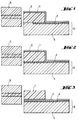
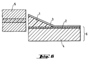
- Fig. 1 which shows an embodiment of the invention, the portion indicated by numeral 6 is the principal lightguide.
- the principal lightguide 6 composed of the lower cladding layer 4 and the lightguiding layer 2 is overlaid with the polymeric optical coupling lightguide 1 which, in turn, is overlaid with the upper cladding layer 3.
- a photopolymerizable monomer or a photocrosslinkable or photopolymerizable polymer or a mixture thereof is applied onto the principal lightguide, and that area of the applied portion where an optical coupling waveguide is to be formed is allowed to cure by exposure through a photomask. Subsequently, the uncured area of the applied portion is removed by treatment with a suitable solvent, thereby providing a polymeric optical coupling waveguide.
- the procedure of applying polymerizable monomers or photocrosslinkable or photopolymerizable polymers is not limited in any particular way and spin coating may typically be employed.
- the first class of materials that may be applied onto the principal lightguide are photopolymerizable monomers and they include the following compounds having a carbon-to-carbon double bond in the molecule: vinyl-containing compounds such as styrene, vinyltoluene, ⁇ -chlorostyrene, isopropylbenzene and 2-vinylpyridine; acrylate compounds such as acrylic acid, 2-ethylhexyl acrylate, n-stearyl acrylate, 2-hydroxyethyl acrylate, 2-hydroxypropyl acrylate, 2-methoxyethyl acrylate, 2-butoxyethyl acrylate, 2-ethoxyethyl acrylate and cyclohexyl acrylate; and methacrylate compounds such as methyl methacrylate, ethyl methacrylate, propyl methacrylate and isopropyl methacrylate.
- vinyl-containing compounds such as styrene, vinyltoluene, ⁇
- the materials from which the polymeric optical coupling waveguide is to be made must have refractive indices that satisfy the optical coupling condition and the liquid mixture described above permits for refractive index control by selecting appropriate types and amounts of crosslinking agents and dyes.
- various solvents such as acetone, methanol, acetonitrile and THF may be used.
- the invention is in no way limited to the photopolymerizable liquid systems exemplified by the liquid mixture described above.
- Other substances that can be used include commercial photocurable clear adhesives (e.g. HARDLOCKTM OP-1000 Series of Denki Kagaku Kogyo K.K.) and the uv curable adhesives described in N. Murata et al., J. Adhesion, vol. 35, 251 (1991).
- the second class of materials that may be applied onto the principal lightguide are photocrosslinkable polymers that may typically have light-sensitive groups as pendants from the backbone chain, which may be provided from the backbone chain, which may be provided from the backbone chain, which may be provided from the following compounds: polyethylenes such as poly(tetrafluoroethylene-co-hexafluoro-propylene) and poly(tetrafluoroethylene); polymethacrylates such as poly(methyl methacrylate), poly(trifluoroethyl methacrylate), poly(cyclohexyl methacrylate), poly(2-chloroethyl methacrylate), poly(2-bromoethyl methacrylate), poly(benzyl methacrylate), poly(phenyl methacrylate), poly(p-bromophenyl methacrylate) and poly(pentachlorophenyl methacrylate); poly( ⁇ -naphthyl methacrylate) and poly(pentabromophen
- Light-sensitive groups are exemplified by a cinnamoyl group, a diazo group, a cinnamylidene group, an acryloyl group, a dithiocarbamate group, and functional groups containing carbon-to-carbon double bonds.
- the third class of materials that may be applied onto the principal lightguide are prepolymers, or photopolymerizable polymers and these are the same as the aforementioned photocrosslinkable polymers, except that the aforementioned light-sensitive groups are attached either as pendants or terminals to the backbone chain of those polymers.
- photopolymerizable monomers or photocrosslinkable or photopolymerizable polymers or mixtures thereof may optionally be mixed with amide-containing photocrosslinking agents such as 2,6-bis(4'-amidobenzoyl)-cyclohexanone, photoradical initiators such as benzyl-dimethylketal, and sensitizers such as Michler's ketone.
- amide-containing photocrosslinking agents such as 2,6-bis(4'-amidobenzoyl)-cyclohexanone
- photoradical initiators such as benzyl-dimethylketal
- sensitizers such as Michler's ketone
- a photosolubilizable polymer is applied onto the principal lightguide and allowed to cure and that area of the applied portion except where a polymeric optical coupling waveguide is to be formed is solubilized by exposure through a photomask. The solubilized area is removed with a suitable solvent, thereby providing a polymeric optical coupling waveguide.
- the procedure of applying the photosolubilizable polymer is not limited in any particular way and spin coating may typically be employed.
- the photosolubilizable polymer include mixtures of alkali-soluble phenolic resins such as cresol novolak with naphthoquinone diazide, and polyamic acid-o-nitrobenzyl alcohol ester.
- the positive-acting resist AZ 1350 commercially available from Hoechst AG may be used.
- the AZ liquid developer of Hoechst AG may be used.
- a polymer that is to form a polymeric optical coupling waveguide is applied onto the principal lightguide and the applied polymer is allowed to cure by a suitable technique and, subsequently, a photoresist is applied onto the cured polymer, which is patterned by a photolithographic technique comprising exposure through a photomask, development and other steps, thereby producing a polymeric optical coupling waveguide.
- photolithographic technique means a common patterning procedure used in the art which comprises a sequence of steps including application of a resist, evaporating the solvent, exposure, development and removal of the resist.
- the resist may be formed of any conventional and common materials for photoresists and it may be either negative- or positive-acting.
- the procedure of applying the polymer also is not limited in any particular way and spin coating may typically be employed.
- the method of forming the polymeric optical coupling waveguide is not limited to the above-described photocuring using photocurable polymers.
- known optical polymers such as PMMA, polycarbonates, polystyrenes, polyamides and polyimides are dissolved in suitable solvents (e.g. cyclohexanone for PMMA) and the resulting solution is spin coated onto the polymeric lightguide device, with the solvent being evaporated in an oven to cure the coating.
- suitable solvents e.g. cyclohexanone for PMMA
- Other materials that may be used are polymers having the backbone chains of the polymers that are used in the aforementioned first method of the invention.
- the refractive indices of these polymers can be finely adjusted by addition of commercial dyes and the like. It should, however, be emphasized that the scope of the invention is in no way limited to the monomers and polymers listed above.
- the principal lightguide is generally comprised of a lower cladding layer and a lightguiding layer or, alternatively, a lower cladding layer, a lightguiding layer and an upper cladding layer.
- the principal lightguide is not limited to any particular type and it may be of a slab or channel type.
- the light-transmitting portion of the principal lightguide, namely, the slab or channel is composed of materials having slightly higher values of refractive index than the surrounding cladding material. If the principal lightguide is of a channel type, various core channels and cladding materials may be combined and typical examples include: CorningTM combined with PyrexTM; glass doped with inorganic ions (e.g.
- the size of the core channel varies greatly depending on whether light propagates in a single mode or a multi mode.
- the size of the core channel also depends on the index difference from the cladding material. The greater the index difference between the core channel of a single-mode waveguide and the cladding material, the smaller the size of the core channel that can be used effectively and vice versa.
- k o is equal to 2 ⁇ / ⁇ ( ⁇ is the wavelength of light)
- T is the thickness of the core channel (or the core layer alone if the lightguide is of a slab type)
- the polymeric optical coupling waveguide may be formed over the lightguiding layer before the latter is overlaid with the upper cladding layer; alternatively, it may be formed over the upper cladding layer after the latter is provided on the lightguiding layer.
- the present invention provides a method of forming the above-described polymeric optical coupling waveguide; additionally, it provides a lightguide device having the polymeric optical coupling waveguide that is formed by this method.
- the polymeric optical coupling waveguide in the lightguiding device of the invention may be tapered in shape.
- the polymeric optical coupling waveguide decreases in width with the increasing distance from an end face.
- the polymeric optical coupling waveguide decreases in thickness with the increasing distance from an end face.
- both the width and the thickness of the polymeric optical coupling waveguide decrease with the increasing distance from an end face.
- the polymeric optical coupling waveguide can easily be tapered in width by selecting an appropriate photomask design.
- One of the following two techniques may be adopted.
- the first technique depends on "dithering" a photomask for producing an optical density profile. Stated more specifically, the polymer or resist becomes thin in the "dark” area of the mask but it is thick in the "light” area.
- Doubleing is a method for controlling the optical density profile by adjusting the number of tiny dots.
- the thus cured product may be developed as it is, thereby creating a taper in thickness.
- the photoresist is first tapered in thickness, then reactive ion etching is conducted to produce the desired shape.
- the second technique of tapering the polymeric optical coupling waveguide involves the use of a mask tapered only in width and performing liquid development (which may be regarded as isotropic etching) to produce a polymeric optical coupling waveguide that is tapered in both width and thickness.
- Polymeric optical coupling waveguides of this geometry may be produced by the combination of the two techniques.
- the lightguiding device of the invention can achieve an even higher optical coupling efficiency if the formation of the polymeric optical coupling waveguide is combined with tapering the area near the entrance and/or exit and faces of the channel lightguiding layer in the principal lightguide. It should be noted here that the polymeric optical coupling waveguide should have a higher refractive index at the exit end face than the channel-type lightguiding layer. Additionally, it is desired that the channel-type lightguiding layer should not be formed far enough to reach the exit end face.
- the lightguide device of the invention is used with particular advantage as a waveguide-type polymeric optically active device which uses the electrooptic effect of polymers as described in C.C. Teng, Appl. Phys. Lett., vol. 60, 1538 (1992).
- Such photoactive devices require lower operating voltages and to this end, the inter-electrode distance must be minimized.
- decreasing the inter-electrode distance means a corresponding decrease in the thickness of the lightguiding layer; in the absence of the optical coupling waveguide, the difficulty in optical coupling from a fiber or LD increases with the decreasing thickness of the lightguiding layer.
- the invention provides ease in coupling a semiconductor laser, a photodiode or fiber optics to lightguiding devices, such as optically active devices of a waveguide type, having the polymeric optical coupling waveguide; further, the invention enables reduction not only in the thickness of the lightguiding layer and the drive voltage.
- Optical coupling as used in the present invention is a technique commonly employed in the art, which is described in prior patents such as Japanese Patent Public Disclosure (kokai) Sho 60-133408, Sho 63-94205 and Hei 4-308803. Several methods of implementing "optical coupling" are described below.
- Refractive index conditions must be satisfied in cases (1) - (5).
- the condition to be satisfied in case (1) is n G > n CP ⁇ n CL , where n CP is the refractive index of the polymeric optical coupling waveguide 1, n G the refractive index of the lightguiding layer 2, and n CL the refractive index of the cladding.
- the condition to be satisfied in cases (2) - (5) is n CP ⁇ n G >n CL . Similar effects are achieved in cases (3) - (5) even if the upper cladding layer is provided between the polymeric optical coupling waveguide 1 and the lightguiding layer 2.
- the latter is desirably subjected to optical polishing with diamond grits.
- the optically polished entrance end face is provided with an anti-reflection coat.
- both an optical fiber and the polymeric optical coupling waveguide are bevelled at an end face by an angle of about 5 degrees in order to reduce reflection of light from end faces.
- a nonlinear optical polymer or a 35/65 (mol/mol)
- P2NAS/MMA copolymer 4-(N,N'-methacryloyl-ethoxy-methylamino)-4'-nitrostilbene/methacrylate copolymer (hereunder abbreviated as "P2NAS/MMA copolymer) was dissolved in cyclohexanone to prepare a 20 % solution, which was spin-coated onto a silicon substrate; then cyclohexanone was evaporated to form a lower cladding layer about 3 ⁇ m thick.
- P2NAS/MMA copolymer 4-(N,N'-methacryloyl-ethoxy-methylamino)-4'-nitrostilbene/methacrylate copolymer
- a 50/50 (mol/mol) P2ANS/MMA copolymer was also dissolved in cyclohexanone to prepare a 20 % solution, which was spin-coated onto the lower cladding layer and cyclohexanone was subsequently evaporated to form a lightguiding layer which was also about 3 ⁇ m thick.
- the lightguiding layer was illuminated with light from a 1000 W xenon lamp through a photomask to form a channel-type lightguide.
- the thus formed channel-type lightguide was spin-coated with a 20/5/1 (wt/wt/wt) MMA/DMPA/PMMA solution through a 0.2 ⁇ m filter.
- the spin-coated film was heated in an oven at 40°C for 1 h and exposed to light from a 1000 W xenon lamp through a photomask.
- the film was further heated in an oven at 100°C for 1 h and developed with methanol. Thereafter, the film was heated on a hot plate at 200°C for 5 min to form a polymeric optical coupling waveguide 30 ⁇ m thick.
- the waveguide in turn was spin-coated with a 40/10/1 (wt/wt/wt) mixture of MMA/DMPA/PMMA in solution and allowed to cure by the same method but without using a photomask to form an upper cladding layer, thereby completing the fabrication of a lightguide device having the same structure as shown in Fig. 1.
- the output power was at least 3 times that of a lightguide device having no optical coupling waveguide.
- a commercial glass lightguide device (Entwicklungsgesellschaft für Integr Of Optik-Technologie GmbH) was spin coated with a commercial photocurable adhesive (HARDLOCKTM OP-1020M of Denki Kagaku Kogyo K.K.) and the resulting coat was cured by exposure to a xenon lamp (1000 W) through a photomask.
- HARDLOCKTM OP-1020M of Denki Kagaku Kogyo K.K.
- the uncured portion of the exposed coat was subjected to development with acetonitrile, thereby forming a polymeric optical coupling waveguide 12 ⁇ m thick that tapered in width. Using this waveguide, a lightguide device was fabricated.
- the entrance end face of the lightguide device fabricated in Example 3 was roughly polished with a lapping film sheet and then finely polished with a diamond slurry. After this end preparation, a semiconductor laser light having a wavelength of 1.3 ⁇ m was directed through a single-mode optical fiber to be launched into the lightguide device. The light issuing from the exit end face was picked up by an objective lens to measure the optical output power.
- the resistance to a displacement for a coupling efficiency of 3 dB was 2.0 ⁇ m in the case of the commercial lightguide device having no polymeric optical coupling waveguide but improved to 4.0 ⁇ m by incorporating the polymeric optical coupling waveguide according to the invention.
- Example 3 The same commercial glass lightguide device as used in Example 3 was spin coated with a positive-acting resist AZ 1350 (Hoechst AG) and the applied coat was cured on a hot plate. The cured coat was exposed to a xenon lamp (1000 W) to solubilize the areas other than the area where a polymeric optical coupling waveguide was to be formed. By development with an AZ liquid developer (Hoechst AG), a polymeric optical coupling waveguide tapering in width was formed. Using this waveguide, a lightguide device was fabricated.
- AZ 1350 Hoechst AG
- the entrance end face of the lightguide device fabricated in Example 5 was roughly polished with a lapping film sheet and then finely polished with a diamond slurry. After this end preparation, a semiconductor laser light having a wavelength of 1.3 ⁇ m was directed through a single-mode optical fiber to be launched into the lightguide device. The light issuing from the exit end face was received by an objective lens to measure the optical output power.
- the resistance to a displacement for a coupling efficiency of 3 dB was 2.0 ⁇ m in the case of the commercial lightguide device having no polymeric optical coupling waveguide but improved to 7.0 ⁇ m by incorporating the polymeric optical coupling waveguide according to the invention.
- Example 3 The same commercial glass lightguide device as used in Example 3 was spin coated with a cyclohexane solution of 10 % PMMA (polymethyl methacrylate) supplemented with an organic dye C.I. Disperse Red 1 for index adjustment.
- PMMA polymethyl methacrylate
- the applied coat was cured by drying in an oven (160°C) for 4 h. Further, the cured coat was patterned as in Example 5 by application of a positive-acting resist (AZ 1350 of Hoechst AG).
- RIE reactive ion etching
- the entrance end face of the lightguide device fabricated in Example 7 was roughly polished with a lapping film sheet and then finely polished with a diamond slurry. After this end preparation, a semiconductor laser light having a wavelength of 1.3 ⁇ m was directed through a single-mode optical fiber to be launched into the lightguide device. The light issuing from the exit end face was picked up by an objective lens to measure the optical output power.
- the resistance to a displacement for a coupling efficiency of 3 dB was 2.0 ⁇ m in the case of the commercial lightguide device having no polymeric optical coupling waveguide but improved to 7.5 ⁇ m by incorporating the polymeric optical coupling waveguide according to the invention.
- Methyl methacrylate (MMA) and glycidyl methacrylate (GMA) were mixed at a molar ratio of 3:7.
- a solvent tetrahydrofuran (THF) was added to the mixture in such an amount that the concentration of the monomer mixture would be about 10 wt %.
- a catalyst 2,2'-azobis(isobutyronitrile) (AIBN) was added to the monomer mixture in an amount of about 2 mol %.
- the resulting mixture was subjected to reaction at 70°C for 5 h in a nitrogen gas atmosphere, thereby yielding a polymer.
- the polymer thus produced was purified by precipitation from methanol. This procedure was repeated about three times.
- the purified polymer was dissolved in toluene and an excess amount of cinnamic acid was dissolved in the solution.
- Example 3 The same commercial glass waveguide as used in Example 3 was dip coated with the polymer solution and the applied coat was dried on a hot plate (90°C) for 3 h to evaporate the solvent, followed by exposure to a xenon lamp (1000 W) for 5 min through a photomask. By subsequent development with a mixed solution of methanol and N-methyl-2-pyrrolidone, a polymeric optical coupling waveguide with a taper in width was formed. Using this waveguide, a lightguide device was fabricated.
- the entrance end face of the lightguide device fabricated in Example 9 was roughly polished with a lapping film sheet and then finely polished with a diamond slurry. After this end preparation, a semiconductor laser light having a wavelength of 1.3 ⁇ m was directed through a single-mode optical fiber to be launched into the lightguide device. The light issuing from the exit end face was picked up by an objective leans to measure the optical output power.
- the resistance to a displacement for a coupling efficiency of 3 dB was 2.0 ⁇ m in the case of the commercial lightguide device having no polymeric optical coupling waveguide but improved to 4.0 ⁇ m by incorporating the polymeric optical coupling waveguide according to the invention.
- the invention achieves a substantial improvement in resistance to displacements and, if the lightguiding is thin, the efficiency of coupling from fiber optics can easily be improved by a factor of at least 3.
Landscapes
- Physics & Mathematics (AREA)
- General Physics & Mathematics (AREA)
- Optics & Photonics (AREA)
- Engineering & Computer Science (AREA)
- Microelectronics & Electronic Packaging (AREA)
- Power Engineering (AREA)
- Optical Integrated Circuits (AREA)
- Optical Couplings Of Light Guides (AREA)
Applications Claiming Priority (2)
| Application Number | Priority Date | Filing Date | Title |
|---|---|---|---|
| JP12652994A JPH07333450A (ja) | 1994-06-08 | 1994-06-08 | 光結合用導波路の形成方法及び光結合用導波路を有する光導波路素子 |
| JP126529/94 | 1994-06-08 |
Publications (2)
| Publication Number | Publication Date |
|---|---|
| EP0687925A2 true EP0687925A2 (de) | 1995-12-20 |
| EP0687925A3 EP0687925A3 (de) | 1996-03-27 |
Family
ID=14937464
Family Applications (1)
| Application Number | Title | Priority Date | Filing Date |
|---|---|---|---|
| EP95108052A Withdrawn EP0687925A3 (de) | 1994-06-08 | 1995-05-26 | Methode zur Herstellung eines optischen Einkoppelwellenleiters und Lichtleiteranordnung mit dem Einkoppelwellenleiter |
Country Status (2)
| Country | Link |
|---|---|
| EP (1) | EP0687925A3 (de) |
| JP (1) | JPH07333450A (de) |
Cited By (16)
| Publication number | Priority date | Publication date | Assignee | Title |
|---|---|---|---|---|
| WO1997028473A1 (de) * | 1996-02-03 | 1997-08-07 | Robert Bosch Gmbh | Verfahren zur herstellung von optischen bauelementen und optisches bauelement |
| WO1998018029A1 (en) * | 1996-10-18 | 1998-04-30 | Telefonaktiebolaget Lm Ericsson (Publ) | Optical guide |
| EP0846968A1 (de) * | 1996-12-03 | 1998-06-10 | Mitsubishi Gas Chemical Company, Inc. | Optisches Verfahren |
| WO1998035250A1 (en) * | 1997-02-07 | 1998-08-13 | Bookham Technology Limited | A tapered rib waveguide |
| RU2151412C1 (ru) * | 1997-03-12 | 2000-06-20 | Самсунг Электроникс Ко., Лтд. | Способ изготовления оптического волноводного устройства |
| GB2350719A (en) * | 1999-06-01 | 2000-12-06 | Bookham Technology Ltd | Joining waveguides on a substrate surface |
| EP1209492A1 (de) * | 2000-11-28 | 2002-05-29 | National University of Ireland Cork | Herstellung von Materialien für Wellenleiter mit Stufenbrechungsindex |
| WO2003048825A1 (en) * | 2001-12-07 | 2003-06-12 | Imego Ab | Method for connecting a fibre optic cable to a light guide |
| WO2004049023A1 (en) * | 2002-11-25 | 2004-06-10 | Tsunami Photonics Limited | Generic waveguide component for planar lightwave circuits |
| US6912345B2 (en) | 2001-03-30 | 2005-06-28 | Shipley Company, L.L.C. | Tapered optical fiber for coupling to diffused optical waveguides |
| EP1512996A4 (de) * | 2002-05-28 | 2005-11-16 | Matsushita Electric Works Ltd | Material für eine gemischt optische/ elektrische substratanbringungs-schaltung und substratanbringung für eine gemischt optische/ elektrische schaltung |
| US6987919B2 (en) | 2000-12-14 | 2006-01-17 | Shipley Company, L.L.C. | Optical waveguide termination with vertical and horizontal mode shaping |
| US7068870B2 (en) | 2000-10-26 | 2006-06-27 | Shipley Company, L.L.C. | Variable width waveguide for mode-matching and method for making |
| US7158701B2 (en) | 2001-02-21 | 2007-01-02 | Shipley Company, L.L.C. | Method for making optical devices with a moving mask and optical devices made thereby |
| US7251406B2 (en) | 2000-12-14 | 2007-07-31 | Shipley Company, L.L.C. | Optical waveguide termination with vertical and horizontal mode shaping |
| EP1921473A4 (de) * | 2005-08-29 | 2010-10-13 | Mitsui Chemicals Inc | Optischer wellenleiterfilm, verfahren zur herstellung des films, den wellenleiterfilm enthaltender optoelektrischer hybridfilm und elektronische einrichtung |
Families Citing this family (4)
| Publication number | Priority date | Publication date | Assignee | Title |
|---|---|---|---|---|
| US6293688B1 (en) * | 1999-11-12 | 2001-09-25 | Sparkolor Corporation | Tapered optical waveguide coupler |
| US7046879B2 (en) * | 2002-11-27 | 2006-05-16 | General Electric Company | Optical via for three dimensional interconnection |
| TWI300141B (en) * | 2005-06-30 | 2008-08-21 | Mitsui Chemicals Inc | Optical waveguide film and optoelectrical hybrid film |
| WO2022259521A1 (ja) * | 2021-06-11 | 2022-12-15 | 日本電信電話株式会社 | 光結合構造およびその製造方法 |
Citations (3)
| Publication number | Priority date | Publication date | Assignee | Title |
|---|---|---|---|---|
| JPS60133408A (ja) | 1983-12-22 | 1985-07-16 | Matsushita Electric Ind Co Ltd | 光結合装置 |
| JPS6394205A (ja) | 1986-10-09 | 1988-04-25 | Hitachi Ltd | 双方向伝送用光励振装置 |
| JPH04308803A (ja) | 1991-04-05 | 1992-10-30 | Nippon Telegr & Teleph Corp <Ntt> | 光導波路形成法 |
Family Cites Families (7)
| Publication number | Priority date | Publication date | Assignee | Title |
|---|---|---|---|---|
| JPS5480144A (en) * | 1977-12-09 | 1979-06-26 | Nec Corp | Integrated thick film photo coupler |
| JPH01316710A (ja) * | 1988-06-17 | 1989-12-21 | Asahi Chem Ind Co Ltd | 新しい光デバイス |
| JPH0312612A (ja) * | 1989-06-09 | 1991-01-21 | Fujitsu Ltd | 光素子間の接続素子 |
| US5054872A (en) * | 1990-03-16 | 1991-10-08 | Ibm Corporation | Polymeric optical waveguides and methods of forming the same |
| DE4111783C1 (de) * | 1991-04-11 | 1992-05-27 | Ant Nachrichtentechnik Gmbh, 7150 Backnang, De | |
| JP3253622B2 (ja) * | 1992-03-07 | 2002-02-04 | ローベルト ボツシユ ゲゼルシヤフト ミツト ベシユレンクテル ハフツング | 光集積回路素子 |
| US5265185A (en) * | 1992-10-02 | 1993-11-23 | The United States Of America As Represented By The Secretary Of The Army | Optical waveguides in electro-optical polymers and method |
-
1994
- 1994-06-08 JP JP12652994A patent/JPH07333450A/ja active Pending
-
1995
- 1995-05-26 EP EP95108052A patent/EP0687925A3/de not_active Withdrawn
Patent Citations (3)
| Publication number | Priority date | Publication date | Assignee | Title |
|---|---|---|---|---|
| JPS60133408A (ja) | 1983-12-22 | 1985-07-16 | Matsushita Electric Ind Co Ltd | 光結合装置 |
| JPS6394205A (ja) | 1986-10-09 | 1988-04-25 | Hitachi Ltd | 双方向伝送用光励振装置 |
| JPH04308803A (ja) | 1991-04-05 | 1992-10-30 | Nippon Telegr & Teleph Corp <Ntt> | 光導波路形成法 |
Non-Patent Citations (2)
| Title |
|---|
| C.C. TENG, APPL. PHYS. LETT., vol. 60, 1992, pages 1538 |
| N. MURATA ET AL., J. ADHESION, vol. 35, 1991, pages 251 |
Cited By (23)
| Publication number | Priority date | Publication date | Assignee | Title |
|---|---|---|---|---|
| US6178281B1 (en) | 1996-02-03 | 2001-01-23 | Robert Bosch Gmbh | Method for the manufacture of optical components, and optical component |
| WO1997028473A1 (de) * | 1996-02-03 | 1997-08-07 | Robert Bosch Gmbh | Verfahren zur herstellung von optischen bauelementen und optisches bauelement |
| WO1998018029A1 (en) * | 1996-10-18 | 1998-04-30 | Telefonaktiebolaget Lm Ericsson (Publ) | Optical guide |
| US6002828A (en) * | 1996-10-18 | 1999-12-14 | Telefonaktiebolaget Lm Ericsson | Polymer optical guide made from a monomer with at least one epoxy group and a vinyl type monomer |
| EP0846968A1 (de) * | 1996-12-03 | 1998-06-10 | Mitsubishi Gas Chemical Company, Inc. | Optisches Verfahren |
| US6052500A (en) * | 1996-12-03 | 2000-04-18 | Mitsubishi Gas Chemical Company, Inc. | Optical waveguide device for connections without optical axis adjustment |
| WO1998035250A1 (en) * | 1997-02-07 | 1998-08-13 | Bookham Technology Limited | A tapered rib waveguide |
| US6108478A (en) * | 1997-02-07 | 2000-08-22 | Bookham Technology Limited | Tapered rib waveguide |
| RU2151412C1 (ru) * | 1997-03-12 | 2000-06-20 | Самсунг Электроникс Ко., Лтд. | Способ изготовления оптического волноводного устройства |
| GB2350719A (en) * | 1999-06-01 | 2000-12-06 | Bookham Technology Ltd | Joining waveguides on a substrate surface |
| US7068870B2 (en) | 2000-10-26 | 2006-06-27 | Shipley Company, L.L.C. | Variable width waveguide for mode-matching and method for making |
| EP1209492A1 (de) * | 2000-11-28 | 2002-05-29 | National University of Ireland Cork | Herstellung von Materialien für Wellenleiter mit Stufenbrechungsindex |
| US6987919B2 (en) | 2000-12-14 | 2006-01-17 | Shipley Company, L.L.C. | Optical waveguide termination with vertical and horizontal mode shaping |
| US7251406B2 (en) | 2000-12-14 | 2007-07-31 | Shipley Company, L.L.C. | Optical waveguide termination with vertical and horizontal mode shaping |
| US7158701B2 (en) | 2001-02-21 | 2007-01-02 | Shipley Company, L.L.C. | Method for making optical devices with a moving mask and optical devices made thereby |
| US6912345B2 (en) | 2001-03-30 | 2005-06-28 | Shipley Company, L.L.C. | Tapered optical fiber for coupling to diffused optical waveguides |
| WO2003048825A1 (en) * | 2001-12-07 | 2003-06-12 | Imego Ab | Method for connecting a fibre optic cable to a light guide |
| EP1512996A4 (de) * | 2002-05-28 | 2005-11-16 | Matsushita Electric Works Ltd | Material für eine gemischt optische/ elektrische substratanbringungs-schaltung und substratanbringung für eine gemischt optische/ elektrische schaltung |
| KR100730320B1 (ko) | 2002-05-28 | 2007-06-19 | 마츠시다 덴코 가부시키가이샤 | 광회로-전기회로 혼재기판용 재료 및 광회로-전기회로혼재기판 |
| US7330612B2 (en) | 2002-05-28 | 2008-02-12 | Matsushita Electric Works, Ltd. | Material for substrate mounting optical circuit-electric circuit mixedly and substrate mounting optical circuit-electric circuit mixedly |
| US8073295B2 (en) | 2002-05-28 | 2011-12-06 | Panasonic Electric Works Co., Ltd. | Material for substrate mounting optical circuit-electrical circuit mixedly and substrate mounting optical circuit-electrical circuit mixedly |
| WO2004049023A1 (en) * | 2002-11-25 | 2004-06-10 | Tsunami Photonics Limited | Generic waveguide component for planar lightwave circuits |
| EP1921473A4 (de) * | 2005-08-29 | 2010-10-13 | Mitsui Chemicals Inc | Optischer wellenleiterfilm, verfahren zur herstellung des films, den wellenleiterfilm enthaltender optoelektrischer hybridfilm und elektronische einrichtung |
Also Published As
| Publication number | Publication date |
|---|---|
| EP0687925A3 (de) | 1996-03-27 |
| JPH07333450A (ja) | 1995-12-22 |
Similar Documents
| Publication | Publication Date | Title |
|---|---|---|
| JPH07333450A (ja) | 光結合用導波路の形成方法及び光結合用導波路を有する光導波路素子 | |
| EP0715726B1 (de) | Polymerische mikrostrukturen,die die kopplung zwischen einer optischen faser und einem wellenleiter vereinfachen | |
| US6549709B1 (en) | Method of making a polymeric optical waveguide device provided with fibre ends, and free-standing, flexible waveguide sheets used therein | |
| US5568579A (en) | Waveguide coupling device including tapered waveguide with a particular tapered angle to reduce coupling loss | |
| JP2915889B2 (ja) | 低損失光能動素子及びその製造方法 | |
| US6266472B1 (en) | Polymer gripping elements for optical fiber splicing | |
| CN114296177A (zh) | 基于二氧化硅/聚合物混合波导的跑道型微环光开关及其制备方法 | |
| US5265185A (en) | Optical waveguides in electro-optical polymers and method | |
| JPH07207470A (ja) | 微細構造の作製方法 | |
| US6037105A (en) | Optical waveguide device fabricating method | |
| Roesch et al. | High-performance low-cost fabrication method for integrated polymer optical devices | |
| CN115877595A (zh) | 一种基于二氧化硅/聚合物混合波导的1×3热光开关及其制备方法 | |
| US5155620A (en) | Nonlinear optical devices and methods | |
| Frish et al. | Rapid photolithographic fabrication of high density optical interconnects using refractive index contrast polymers | |
| US20030123806A1 (en) | Integrated optical devices and method of fabrication therefor | |
| Watanabe et al. | Novel ‘‘serially grafted’’connection between functional and passive polymer waveguides | |
| Oh et al. | Low-loss interconnection between electrooptic and passive polymer waveguides with a vertical taper | |
| CN115755272B (zh) | 一种聚合物/氮化硅混合集成的可变光衰减器及其制备方法 | |
| JPH10170738A (ja) | 高分子光導波路及びその作製方法 | |
| EP0464795B1 (de) | Nichtlineare optische Materialien und Vorrichtungen | |
| Najafi et al. | Integrated optics devices by ultraviolet light imprinting in sol-gel silica glass | |
| JPH10170739A (ja) | 高分子光導波路及びその作製方法 | |
| KR100426959B1 (ko) | 평판형 광도파로의 제조방법 | |
| Pun et al. | Polymeric waveguides and devices for integrated optics applications | |
| JP3343849B2 (ja) | 高分子光導波路及びその作製方法 |
Legal Events
| Date | Code | Title | Description |
|---|---|---|---|
| PUAI | Public reference made under article 153(3) epc to a published international application that has entered the european phase |
Free format text: ORIGINAL CODE: 0009012 |
|
| AK | Designated contracting states |
Kind code of ref document: A2 Designated state(s): DE FR GB IT NL |
|
| PUAL | Search report despatched |
Free format text: ORIGINAL CODE: 0009013 |
|
| AK | Designated contracting states |
Kind code of ref document: A3 Designated state(s): DE FR GB IT NL |
|
| 17P | Request for examination filed |
Effective date: 19960927 |
|
| RAP1 | Party data changed (applicant data changed or rights of an application transferred) |
Owner name: AVENTIS RESEARCH & TECHNOLOGIES GMBH & CO. KG |
|
| RAP1 | Party data changed (applicant data changed or rights of an application transferred) |
Owner name: AXIVA GMBH |
|
| RAP1 | Party data changed (applicant data changed or rights of an application transferred) |
Owner name: CELANESE VENTURES GMBH |
|
| 17Q | First examination report despatched |
Effective date: 20010515 |
|
| STAA | Information on the status of an ep patent application or granted ep patent |
Free format text: STATUS: THE APPLICATION HAS BEEN WITHDRAWN |
|
| 18W | Application withdrawn |
Withdrawal date: 20010811 |