EP0687992B1 - Modulateur de lumière avec un arrangement de laser pour exposer des données d'images - Google Patents
Modulateur de lumière avec un arrangement de laser pour exposer des données d'images Download PDFInfo
- Publication number
- EP0687992B1 EP0687992B1 EP95201467A EP95201467A EP0687992B1 EP 0687992 B1 EP0687992 B1 EP 0687992B1 EP 95201467 A EP95201467 A EP 95201467A EP 95201467 A EP95201467 A EP 95201467A EP 0687992 B1 EP0687992 B1 EP 0687992B1
- Authority
- EP
- European Patent Office
- Prior art keywords
- light
- modulator
- light modulator
- exposure system
- modulation
- Prior art date
- Legal status (The legal status is an assumption and is not a legal conclusion. Google has not performed a legal analysis and makes no representation as to the accuracy of the status listed.)
- Expired - Lifetime
Links
Images

Classifications
-
- H—ELECTRICITY
- H04—ELECTRIC COMMUNICATION TECHNIQUE
- H04N—PICTORIAL COMMUNICATION, e.g. TELEVISION
- H04N1/00—Scanning, transmission or reproduction of documents or the like, e.g. facsimile transmission; Details thereof
- H04N1/04—Scanning arrangements, i.e. arrangements for the displacement of active reading or reproducing elements relative to the original or reproducing medium, or vice versa
- H04N1/19—Scanning arrangements, i.e. arrangements for the displacement of active reading or reproducing elements relative to the original or reproducing medium, or vice versa using multi-element arrays
- H04N1/191—Scanning arrangements, i.e. arrangements for the displacement of active reading or reproducing elements relative to the original or reproducing medium, or vice versa using multi-element arrays the array comprising a one-dimensional [1D] array
- H04N1/192—Simultaneously or substantially simultaneously scanning picture elements on one main scanning line
- H04N1/193—Simultaneously or substantially simultaneously scanning picture elements on one main scanning line using electrically scanned linear arrays, e.g. linear CCD arrays
-
- B—PERFORMING OPERATIONS; TRANSPORTING
- B41—PRINTING; LINING MACHINES; TYPEWRITERS; STAMPS
- B41J—TYPEWRITERS; SELECTIVE PRINTING MECHANISMS, i.e. MECHANISMS PRINTING OTHERWISE THAN FROM A FORME; CORRECTION OF TYPOGRAPHICAL ERRORS
- B41J2/00—Typewriters or selective printing mechanisms characterised by the printing or marking process for which they are designed
- B41J2/435—Typewriters or selective printing mechanisms characterised by the printing or marking process for which they are designed characterised by selective application of radiation to a printing material or impression-transfer material
- B41J2/447—Typewriters or selective printing mechanisms characterised by the printing or marking process for which they are designed characterised by selective application of radiation to a printing material or impression-transfer material using arrays of radiation sources
- B41J2/45—Typewriters or selective printing mechanisms characterised by the printing or marking process for which they are designed characterised by selective application of radiation to a printing material or impression-transfer material using arrays of radiation sources using light-emitting diode [LED] or laser arrays
- B41J2/451—Special optical means therefor, e.g. lenses, mirrors, focusing means
-
- B—PERFORMING OPERATIONS; TRANSPORTING
- B41—PRINTING; LINING MACHINES; TYPEWRITERS; STAMPS
- B41J—TYPEWRITERS; SELECTIVE PRINTING MECHANISMS, i.e. MECHANISMS PRINTING OTHERWISE THAN FROM A FORME; CORRECTION OF TYPOGRAPHICAL ERRORS
- B41J2/00—Typewriters or selective printing mechanisms characterised by the printing or marking process for which they are designed
- B41J2/435—Typewriters or selective printing mechanisms characterised by the printing or marking process for which they are designed characterised by selective application of radiation to a printing material or impression-transfer material
- B41J2/465—Typewriters or selective printing mechanisms characterised by the printing or marking process for which they are designed characterised by selective application of radiation to a printing material or impression-transfer material using masks, e.g. light-switching masks
-
- G—PHYSICS
- G06—COMPUTING OR CALCULATING; COUNTING
- G06K—GRAPHICAL DATA READING; PRESENTATION OF DATA; RECORD CARRIERS; HANDLING RECORD CARRIERS
- G06K15/00—Arrangements for producing a permanent visual presentation of the output data, e.g. computer output printers
- G06K15/02—Arrangements for producing a permanent visual presentation of the output data, e.g. computer output printers using printers
- G06K15/12—Arrangements for producing a permanent visual presentation of the output data, e.g. computer output printers using printers by photographic printing, e.g. by laser printers
- G06K15/1238—Arrangements for producing a permanent visual presentation of the output data, e.g. computer output printers using printers by photographic printing, e.g. by laser printers simultaneously exposing more than one point
- G06K15/1242—Arrangements for producing a permanent visual presentation of the output data, e.g. computer output printers using printers by photographic printing, e.g. by laser printers simultaneously exposing more than one point on one main scanning line
- G06K15/1252—Arrangements for producing a permanent visual presentation of the output data, e.g. computer output printers using printers by photographic printing, e.g. by laser printers simultaneously exposing more than one point on one main scanning line using an array of light modulators, e.g. a linear array
Definitions
- This invention relates to printing systems capable of developing an image and, more particularly, to a light modulation and exposure system for exposing light sensitive material with image data.
- a typical laser printer radiation from laser is shaped, and imaged onto the film plane to produce the desired spot size.
- the spot forms the smallest element of the image, called "pixel".
- the laser radiation is modulated in an imagewise fashion to create right image density, pixel by pixel.
- the laser spot is scanned in line and page directions to create a two-dimensional image. If a continuous wave (CW) type gas or solid state laser is used, an external modulator of Acousto-Optic or Electro-Optic type is favored; for semiconductor diode lasers, laser radiation is modulated by varying the current input to the laser.
- CW continuous wave
- semiconductor diode lasers laser radiation is modulated by varying the current input to the laser.
- high throughput is obtained by scanning the laser beam in the line direction by a rotating polygonal mirror, a galvanometer or a hologonal diffractive element, also called "flying spot" printers.
- low sensitivity media printer such as a laser thermal printer
- higher power lasers are used and exposure requirements of the order of 0.5 joules/cm 2 are met by scanning the laser beam slowly in both line and page directions.
- One way to achieve this is to configure the printer like a "lathe", where line scan is obtained by a rotating drum which holds the film and page scan by translating the laser or drum in the direction along the axis of rotation.
- United States Patent No. 5,132,723 is directed to a method and apparatus for controlling exposure using light valves.
- the light valve is being imaged onto an object, for example, a sheet of light-sensitive material and the image is scanned along the object either by moving the object or the image.
- Such an arrangement allows for the correction of exposure and/or compensation for any dead sites.
- such a practice clearly reduces the total throughput of data and requires complicated, individualized calibration techniques to compensate and adjust the exposure for each site in the array.
- United States Patent No. 5,049,901 relates to a light modulator that uses large area light sources such as an arc lamp to image onto a two-dimensional light valve, preferably of the deformable mirror type.
- the light valve is imaged onto a light-sensitive material and the image is scanned along the light-sensitive material. Because the light source is a broad spectrum source, the light valve will absorb energy near the fringes that will result in elevating the operating temperature of the light valve. Because the medium has a limited absorption band energy in that band, it will be used for writing, but a substantial portion of that energy will be absorbed by the light valve.
- the preferred way of operation requires that a substantial amount of the energy available in a light source should be used for writing purposes and not to raise the temperature of the equipment and surroundings.
- United States Patent No. 5,208,818 is directed to a laser system for recording data patterns on a planar substrate.
- a deformable mirror spatial light modulator is used together with a waveguide-type excimer laser to record a large number of data bits with each laser pulse.
- This is an ultraviolet (UV) pulsed excimer laser and uses a medium having a thin ablatable coating on a quartz substrate. Multiple exposures by the pulsed laser is used on the modulator to reduce average power density on the modulator.
- UV ultraviolet
- the pulsed laser is used on the modulator to reduce average power density on the modulator.
- Such a system can find use in the manufacture of circuit boards using photoresist.
- the present invention uses a constant wave (CW) source for thermal transfer or removal of thermal dyes to record images.
- CW constant wave
- Laser array is used as the illumination source.
- a reflective or transmittive modulator is illuminated uniformly by the light from all elements of laser.
- the elements of the modulator break up the light beam in image elements.
- Each element of the modulator is subsequently imaged on the film plane to form desired size spots.
- the modulator can be of a linear or area type with a variety of element densities. Examples of modulators are PLZT, liquid crystal, deflecting, deformable mirrors and elastomers, etc. Modulation characteristics of each modulator element enables image pixel density.
- the original generator includes an optical schlieren system and an active matrix-addressable surface light modulator which has a visco-elastic control film with a reflective surface.
- a mirror Disposed between the schlieren lens and the projection lens in the schlieren system is a mirror which preferably has two functions, not only reflecting the light from the light source to the light modulator but also filtering out undiffracted reflected light.
- the schlieren lens is located at a distance from the light modulator which is short relative to the focal length of the lens.
- a positioning table designed to hold the pattern or the electronic element is disposed in such a way that sharp images of areas on the surface of the light modulator can be produced on the pattern or the electronic element.
- the image pixel information comes from the modulator, not the laser.
- the laser array acts as the uniform high power illumination source. All elements are activated simultaneously with one power supply and provide a CW level power output. This is particularly useful when used for laser thermal printing as it is not possible to obtain such high powers with single elements.
- a plurality of diode lasers S1, S2, S3, S4 ... S10 form a laser array shown generally at 10.
- the elements of the array are activated simultaneously using a common power supply (not shown) in a CW manner.
- CW laser and non-individually modulated operation of the laser simplifies the power supply and heat dissipation mechanism which can take a variety of forms generally used in these devices.
- All elements of the array 10 illuminate a line or area of a specified size on a specified plane.
- the illumination optics as shown in Figure 1 can take a variety of forms, from conventional discreet elements to binary optics to a combination thereof to achieve a desired line or area illumination on the modulator.
- an array of lenslets 12 are positioned in front of the laser array 10 where the light from each laser diode S1-S10 in the laser array 10 passes through its corresponding lenslet 12.
- the lenslet array 12 has power in the array direction and substantially no power in the cross-array direction.
- a field lens 14 is used to focus the respective light beams on a modulator 16.
- Figure 1 shows the use of a transmittive type modulator array 16 with a number of elements configured in modulator array 16.
- a linear array is shown in Figure 1 and could be a whole print line or only a few elements of the line, an area or a combination thereof.
- Elements of the modulator array 16 form individual pixels of the image, the diode array could also take the form of a laser bar.
- Example of modulators are PLZT, liquid crystal type, electro-optics, acousto-optic type, magneto-optic and any other kind which modulates the light transmitted through it.
- the size and shape of each element is determined by the characteristics of the modulator, characteristics of the image and desired modulation rate.
- the light beams after passing through elements of the modulator array 16 are imaged by imaging optics 18 on the film plane 20.
- the elements are magnified or de-magnified in either direction using anamorphic optics 14 and 18, respectively, depending on the spot size requirement of the light beam at the film plane 20. Both the size and the pitch of the spots can be controlled by appropriately configuring the elements in the modulator array 16 in connection with the choice of imaging optics.
- the elements in the modulator array are individually modulatable and provide the right image density for each pixel.
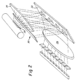
- a second embodiment is shown in Figure 2.
- a reflective modulator array 22 is used.
- the mechanism for generating pixels in an image is similar to the one discussed in the first embodiment except that light is reflected instead of transmitted from each element in the modulator array 22.
- Examples of such reflective modulators include PLZT, liquid crystals, light valves, A-0, and E-0 types. Again, the modulation rate is governed by the characteristics of the modulator array 22. The pixel size and pixel density are dependent upon the array configuration and imaging optics 24.
- a special kind of reflective modulator array 22 is based on deformable mirror, deflecting mirror, gratings, elastomers, etc.
- An example of a deformable mirror is manufactured by Texas Instrument, Inc.
- the modulator array 22 takes the form of a series of mirrors or mirror-like devices which are configured in a linear array. The whole modulator array 22 is uniformly illuminated by illumination optics 26 and each mirror in the modulator array 22 which forms a pixel that is imaged on the film plane 28.
- each mirror element When a pixel address electrode is energized, each mirror element either deflects or deforms under an electrostatic force that changes the direction of the light being reflected. The reflected light can be captured by a stop 30 and prevented from reaching the film plane 28.
- the normal state could be the reflection of light to the stop 30 and not having it reach the film plane 28.
- the corresponding mirror element is rotated or deformed for a desired time to expose the film at the film plane 28 and then reverts back to the non-exposure normal state.
- a gray level of the image can be obtained by timing the exposure of each pixel. This is the equivalent of pulse width modulation of the diode laser device and the response time depends on characteristics of the device. In some cases, the equivalent of amplitude modulation can be achieved by only partially distorting or rotating the mirror. In this way, only a portion of the light makes it to the film plane 28. The gray level can be achieved by controlling the portion of the light making to the film plane.
- the same type of operational mechanism applies to a grating, an elastomer and other devices.
- the high reflectivity is obtained by appropriately coating the mirror surface for the right wavelength.
- a whole line or, alternatively, a few pixels of a line can be written using a linear modulator array of elements; or a whole area of the image or a part thereof can be written using an area array of modulator elements.
- the resolution of the image can be zoomed electronically by ganging together of a few elements of the modulator, i.e., supplying them the same pixel data. Effectively a larger pixel size can be achieved this way with the same optical configuration.
- By shifting modulation operation from the laser to the modulator array high speed operation can be obtained by easily controlling low levels of voltage and current without any thermal and electrical cross-talk.
- the overall illumination intensity can be maintained by appropriately increasing the current to another element of the laser.
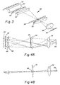
- Figure 3 is a perspective view diagrammatic configuration of a preferred embodiment which also serves as a more detailed example.
- FIG. 4 shows elevational and plane view of this configuration.
- the diode laser bar 40 has 12 emitters with spacing dimension of 200 microns in the array direction and 1 micron in the cross-array direction at 800 microns pitch.
- a rod lens 42 placed about a mm away from the diode array is used to collect light from the cross-array direction of the laser.
- a cylindrical lenslet array 44 is used to collimate the laser radiation. The lenslet array 44 is placed about 5mm from the laser array.
- a field combiner lens 46 is used to combine light from all the emitters of the laser array and illuminate the transmissive modulator 48.
- the modulator 48 has about 120 channels and is placed about 250mm from the lenslet array 44.
- the total size of the modulator 48 is about 10mm and the size of each element of the modulator is 80 microns by 40 microns with fill factor of about 80%.
- the field lens 50 in combination with the printing lens 54 provides the image of modulator 48 on the film plane 56 to create writing spots.
- the de-magnification is about 16 times and the numerical aperture of the spots is about 0.32.
- the spot size is about 5 microns by 2.5 microns.
- Each element of the modulator is modulated in the imagewise fashion to generate the desired image.
Landscapes
- Physics & Mathematics (AREA)
- Engineering & Computer Science (AREA)
- Optics & Photonics (AREA)
- General Health & Medical Sciences (AREA)
- Signal Processing (AREA)
- Health & Medical Sciences (AREA)
- Multimedia (AREA)
- Toxicology (AREA)
- General Engineering & Computer Science (AREA)
- General Physics & Mathematics (AREA)
- Theoretical Computer Science (AREA)
- Printers Or Recording Devices Using Electromagnetic And Radiation Means (AREA)
- Laser Beam Printer (AREA)
- Exposure And Positioning Against Photoresist Photosensitive Materials (AREA)
Claims (9)
- Système d'exposition et de modulation de lumière destiné à exposer un matériau photosensible (20, 28, 56) avec des données d'image, ledit système comprenant un modulateur de lumière linéaire (16, 22, 48) comportant une rangée d'éléments de modulation de lumière, ledit modulateur de lumière linéaire étant positionné de sorte qu'une pluralité de sources de lumière laser (51 à 54) illuminent les éléments de modulation de lumière, des éléments optiques d'illumination (12, 14, 26, 42, 44, 46) situés entre ladite pluralité de sources de lumière laser (51 à 54) et ledit modulateur de lumière linéaire (16, 22, 48), et un moyen (18, 24, 50, 54) destiné à focaliser la lumière provenant dudit modulateur de lumière linéaire (16, 22, 48), caractérisé en ce que lesdits éléments optiques d'illumination sont constitués de : un réseau de micro-lentilles (12, 44) et d'une lentille de champ (14, 26, 46).
- Système d'exposition et de modulation de lumière selon la revendication 1, caractérisé en outre par : un moyen destiné à générer un mouvement relatif entre la lumière provenant dudit modulateur de lumière et le matériau photosensible, la direction dudit mouvement étant sensiblement perpendiculaire à la direction de ladite rangée d'éléments de modulation de lumière à un débit d'une ligne de données d'image à la fois, et un moyen destiné à transférer dans la rangée d'éléments de modulation de lumière les données à former en image sur ledit matériau photosensible une ligne à la fois.
- Système d'exposition et de modulation de lumière selon la revendication 1, dans lequel la pluralité de micro-lentilles est prévue pour mettre en forme chaque faisceau de lumière provenant de la source de lumière laser correspondante.
- Système d'exposition et de modulation de lumière selon la revendication 1, dans lequel les éléments de modulation de lumière sont des miroirs déformables commandés électriquement.
- Système d'exposition et de modulation de lumière selon la revendication 4, dans lequel le modulateur de lumière est commandé d'une manière selon laquelle seuls les miroirs déformables activés par les données résulteront en une lumière atteignant un matériau photosensible.
- Système d'exposition et de modulation de lumière selon la revendication 1, dans lequel le modulateur de lumière est du type à cristaux liquides.
- Système d'exposition et de modulation de lumière selon la revendication 1, dans lequel le modulateur de lumière est du type magnéto-optique.
- Système d'exposition et de modulation de lumière selon la revendication 1, dans lequel le modulateur de lumière est du type ferroélectrique.
- Système d'exposition et de modulation de lumière selon la revendication 1, dans lequel le modulateur de lumière est un modulateur de lumière à deux dimensions.
Applications Claiming Priority (2)
| Application Number | Priority Date | Filing Date | Title |
|---|---|---|---|
| US08/261,370 US5521748A (en) | 1994-06-16 | 1994-06-16 | Light modulator with a laser or laser array for exposing image data |
| US261370 | 1994-06-16 |
Publications (2)
| Publication Number | Publication Date |
|---|---|
| EP0687992A1 EP0687992A1 (fr) | 1995-12-20 |
| EP0687992B1 true EP0687992B1 (fr) | 2002-05-15 |
Family
ID=22993006
Family Applications (1)
| Application Number | Title | Priority Date | Filing Date |
|---|---|---|---|
| EP95201467A Expired - Lifetime EP0687992B1 (fr) | 1994-06-16 | 1995-06-03 | Modulateur de lumière avec un arrangement de laser pour exposer des données d'images |
Country Status (4)
| Country | Link |
|---|---|
| US (1) | US5521748A (fr) |
| EP (1) | EP0687992B1 (fr) |
| JP (1) | JP3255825B2 (fr) |
| DE (1) | DE69526696T2 (fr) |
Families Citing this family (143)
| Publication number | Priority date | Publication date | Assignee | Title |
|---|---|---|---|---|
| JPH0825686A (ja) * | 1994-07-11 | 1996-01-30 | Canon Inc | 画像形成装置 |
| GB2296098B (en) * | 1994-12-15 | 1998-02-11 | British Aerospace | Optical cross bar switch assembly |
| US6088532A (en) * | 1995-01-06 | 2000-07-11 | Asahi Kogaku Kogyo Kabushiki Kaisha | Image signal reading operation control device |
| US5825552A (en) * | 1995-03-24 | 1998-10-20 | Eastman Kodak Company | Beamsplitter/staggerer for multi-beam laser printers |
| US5646713A (en) * | 1995-06-13 | 1997-07-08 | Eastman Kodak Company | Apparatus and method for exposing data characters onto a strip region of moving photosensitive media |
| JPH09234579A (ja) * | 1996-02-28 | 1997-09-09 | Semiconductor Energy Lab Co Ltd | レーザー照射装置 |
| US6268893B1 (en) * | 1996-03-11 | 2001-07-31 | American Bank Note Holographics | Method and apparatus for a fringe direct writing system |
| US5969741A (en) * | 1996-06-17 | 1999-10-19 | Xerox Corporation | Raster scanner with a selectable spot dimension |
| US5808657A (en) * | 1996-06-17 | 1998-09-15 | Eastman Kodak Company | Laser printer with low fill modulator array and high pixel fill at a media plane |
| JP3628448B2 (ja) * | 1996-08-07 | 2005-03-09 | 富士写真フイルム株式会社 | 露光装置 |
| US5790310A (en) * | 1996-10-28 | 1998-08-04 | Lucent Technologies Inc. | Lenslet module for coupling two-dimensional laser array systems |
| US5923475A (en) * | 1996-11-27 | 1999-07-13 | Eastman Kodak Company | Laser printer using a fly's eye integrator |
| US5982553A (en) | 1997-03-20 | 1999-11-09 | Silicon Light Machines | Display device incorporating one-dimensional grating light-valve array |
| US5764280A (en) * | 1997-03-20 | 1998-06-09 | Silicon Light Machines Inc. | Display system including an image generator and movable scanner for same |
| US5900981A (en) * | 1997-04-15 | 1999-05-04 | Scitex Corporation Ltd. | Optical system for illuminating a spatial light modulator |
| DE19715807C1 (de) | 1997-04-16 | 1999-01-28 | Vitaly Dr Lissotschenko | Vorrichtung zur Erzeugung von Gitterstrukturen in Lichtleitfasern |
| IL120841A (en) * | 1997-05-16 | 2001-07-24 | Creoscitex Corp Ltd | Writing heads with an array of laser diodes that can be turned separately |
| US5861992A (en) * | 1997-06-20 | 1999-01-19 | Creo Products Inc | Microlensing for multiple emitter laser diodes |
| US6240116B1 (en) | 1997-08-14 | 2001-05-29 | Sdl, Inc. | Laser diode array assemblies with optimized brightness conservation |
| US6310712B1 (en) | 1997-10-29 | 2001-10-30 | Teloptics Corporation | Discrete element light modulating microstructure devices |
| US6768572B2 (en) | 1997-10-29 | 2004-07-27 | Teloptics Corporation | Solid state free space switch array on a substrate |
| US6816296B2 (en) | 1997-10-29 | 2004-11-09 | Teloptics Corporation | Optical switching network and network node and method of optical switching |
| US6166759A (en) * | 1998-04-07 | 2000-12-26 | Eastman Kodak Company | Bent smile corrector |
| US6084626A (en) * | 1998-04-29 | 2000-07-04 | Eastman Kodak Company | Grating modulator array |
| US6593064B1 (en) * | 1998-06-19 | 2003-07-15 | Creo Inc. | High resolution optical stepper |
| US6130770A (en) | 1998-06-23 | 2000-10-10 | Silicon Light Machines | Electron gun activated grating light valve |
| US6101036A (en) | 1998-06-23 | 2000-08-08 | Silicon Light Machines | Embossed diffraction grating alone and in combination with changeable image display |
| US6303986B1 (en) | 1998-07-29 | 2001-10-16 | Silicon Light Machines | Method of and apparatus for sealing an hermetic lid to a semiconductor die |
| US6872984B1 (en) | 1998-07-29 | 2005-03-29 | Silicon Light Machines Corporation | Method of sealing a hermetic lid to a semiconductor die at an angle |
| US6215598B1 (en) * | 1998-10-05 | 2001-04-10 | Ruey Jennifer Hwu | Apparatus and method for concentrating beams from broad area diode lasers, diode laser bars and/ or diode laser arrays |
| US6204875B1 (en) | 1998-10-07 | 2001-03-20 | Barco Graphics, Nv | Method and apparatus for light modulation and exposure at high exposure levels with high resolution |
| US6486996B1 (en) | 1998-10-27 | 2002-11-26 | Teloptics Corporations | Discrete element light modulating microstructure devices |
| US6005717A (en) * | 1998-11-17 | 1999-12-21 | Ceramoptec Industries, Inc. | Diode laser beam combiner system |
| US6215547B1 (en) | 1998-11-19 | 2001-04-10 | Eastman Kodak Company | Reflective liquid crystal modulator based printing system |
| US6121983A (en) * | 1998-11-19 | 2000-09-19 | Xerox Corporation | Method and apparatus for a solid state laser scanning architecture |
| US6064528A (en) * | 1998-11-20 | 2000-05-16 | Eastman Kodak Company | Multiple laser array sources combined for use in a laser printer |
| US6079833A (en) | 1999-02-17 | 2000-06-27 | Hughes-Jvc Technology Corporation | Laser imaging using a spatial light modulator |
| US6169565B1 (en) | 1999-03-31 | 2001-01-02 | Eastman Kodak Company | Laser printer utilizing a spatial light modulator |
| US6211997B1 (en) | 1999-03-31 | 2001-04-03 | Eastman Kodak Company | Modulator for optical printing |
| US6266080B1 (en) * | 1999-04-30 | 2001-07-24 | Creo Srl | Thermal recording with variable power density |
| US6407849B1 (en) | 1999-07-01 | 2002-06-18 | Creoscitex Corporation Ltd | Method and system for illumination using laser diode bar and microlenses array of same pitch |
| US6229650B1 (en) | 1999-10-18 | 2001-05-08 | Agfa Corporation | Optical imaging head having a multiple writing bean source |
| US6330018B1 (en) | 1999-12-22 | 2001-12-11 | Eastman Kodak Company | Method and apparatus for printing high resolution images using reflective LCD modulators |
| US6478452B1 (en) | 2000-01-19 | 2002-11-12 | Coherent, Inc. | Diode-laser line-illuminating system |
| US6956878B1 (en) | 2000-02-07 | 2005-10-18 | Silicon Light Machines Corporation | Method and apparatus for reducing laser speckle using polarization averaging |
| US6494371B1 (en) | 2000-03-09 | 2002-12-17 | Coherent, Inc. | Diode-laser light projector for illuminating a linear array of light modulators |
| US6396530B1 (en) | 2000-06-12 | 2002-05-28 | Eastman Kodak Company | Method for improving exposure resolution using multiple exposures |
| US6943919B1 (en) | 2000-06-29 | 2005-09-13 | Eastman Kodak Company | Method and apparatus for correcting defects in a spatial light modulator based printing system |
| DE10031915A1 (de) * | 2000-06-30 | 2002-01-10 | Heidelberger Druckmasch Ag | Kompakte Mehrstrahllaserlichtquelle und Interleafrasterscanlinien-Verfahren zur Belichtung von Druckplatten |
| DE20023981U1 (de) | 2000-06-30 | 2008-06-19 | Heidelberger Druckmaschinen Ag | Kompakte Mehrstrahllaserlichtquelle zur Belichtung von Druckplatten |
| US6407766B1 (en) | 2000-07-18 | 2002-06-18 | Eastman Kodak Company | Method and apparatus for printing to a photosensitive media using multiple spatial light modulators |
| US6646716B1 (en) | 2000-07-27 | 2003-11-11 | Eastman Kodak Company | Method and apparatus for printing multiple simultaneous images onto a photosensitive media |
| US6552740B1 (en) | 2000-08-01 | 2003-04-22 | Eastman Kodak Company | Method and apparatus for printing monochromatic imaging using a spatial light modulator |
| US6433934B1 (en) | 2000-08-11 | 2002-08-13 | Yakov Reznichenko | Illumination system for use in imaging systems |
| JP2002072132A (ja) * | 2000-08-30 | 2002-03-12 | Dainippon Screen Mfg Co Ltd | 照明装置 |
| US6480259B1 (en) | 2000-09-28 | 2002-11-12 | Eastman Kodak Company | Method and apparatus for printing monochromatic images using a spatial light modulator having a selectable light source |
| US6614462B1 (en) | 2000-10-19 | 2003-09-02 | Eastman Kodak Company | Method and apparatus for printing high resolution images using reflective LCD modulators |
| US6580490B1 (en) | 2000-10-30 | 2003-06-17 | Eastman Kodak Company | Method and apparatus for printing images in multiple formats using a spatial light modulator |
| DE10054950A1 (de) * | 2000-11-06 | 2002-05-08 | Lissotschenko Vitalij | Vorrichtung zur Abbildung modulierten Lichts auf ein thermisch sensitives Medium |
| EP1215523A3 (fr) * | 2000-12-16 | 2004-05-26 | Hentze-Lissotschenko Patentverwaltungs GmbH & Co.KG | Système d'irradiation avec transformation du faisceau pour générer une radiation modulée |
| DE10108624A1 (de) | 2001-02-22 | 2002-09-05 | Heidelberger Druckmasch Ag | Banding-reduzierende Bebilderung einer Druckform |
| US6930797B2 (en) | 2001-02-27 | 2005-08-16 | Eastman Kodak Company | Method and apparatus for printing high resolution images using multiple reflective spatial light modulators |
| US7177081B2 (en) | 2001-03-08 | 2007-02-13 | Silicon Light Machines Corporation | High contrast grating light valve type device |
| US6707591B2 (en) | 2001-04-10 | 2004-03-16 | Silicon Light Machines | Angled illumination for a single order light modulator based projection system |
| US6865346B1 (en) | 2001-06-05 | 2005-03-08 | Silicon Light Machines Corporation | Fiber optic transceiver |
| US6782205B2 (en) | 2001-06-25 | 2004-08-24 | Silicon Light Machines | Method and apparatus for dynamic equalization in wavelength division multiplexing |
| US6747781B2 (en) | 2001-06-25 | 2004-06-08 | Silicon Light Machines, Inc. | Method, apparatus, and diffuser for reducing laser speckle |
| US6829092B2 (en) | 2001-08-15 | 2004-12-07 | Silicon Light Machines, Inc. | Blazed grating light valve |
| US6980321B2 (en) | 2001-08-20 | 2005-12-27 | Eastman Kodak Company | Method and apparatus for printing high resolution images using multiple reflective spatial light modulators |
| US6930364B2 (en) | 2001-09-13 | 2005-08-16 | Silicon Light Machines Corporation | Microelectronic mechanical system and methods |
| US6980280B2 (en) * | 2001-10-12 | 2005-12-27 | Eastman Kodak Company | Two level image writer |
| US6574043B2 (en) | 2001-11-07 | 2003-06-03 | Eastman Kodak Company | Method for enhanced bit depth in an imaging apparatus using a spatial light modulator |
| US6956995B1 (en) | 2001-11-09 | 2005-10-18 | Silicon Light Machines Corporation | Optical communication arrangement |
| US6800238B1 (en) | 2002-01-15 | 2004-10-05 | Silicon Light Machines, Inc. | Method for domain patterning in low coercive field ferroelectrics |
| US6574032B1 (en) | 2002-01-23 | 2003-06-03 | Eastman Kodak Company | Imaging apparatus using dither to minimize pixel effects |
| US6582875B1 (en) | 2002-01-23 | 2003-06-24 | Eastman Kodak Company | Using a multichannel linear laser light beam in making OLED devices by thermal transfer |
| US6900826B2 (en) * | 2002-02-19 | 2005-05-31 | Presstek, Inc. | Multiple resolution helical imaging system and method |
| CA2418294A1 (fr) * | 2002-03-08 | 2003-09-08 | Heidelberger Druckmaschinen Aktiengesellschaft | Methode d'imagerie pour formes d'impression |
| US6728023B1 (en) | 2002-05-28 | 2004-04-27 | Silicon Light Machines | Optical device arrays with optimized image resolution |
| US6767751B2 (en) | 2002-05-28 | 2004-07-27 | Silicon Light Machines, Inc. | Integrated driver process flow |
| US7054515B1 (en) | 2002-05-30 | 2006-05-30 | Silicon Light Machines Corporation | Diffractive light modulator-based dynamic equalizer with integrated spectral monitor |
| US6822797B1 (en) | 2002-05-31 | 2004-11-23 | Silicon Light Machines, Inc. | Light modulator structure for producing high-contrast operation using zero-order light |
| US6829258B1 (en) | 2002-06-26 | 2004-12-07 | Silicon Light Machines, Inc. | Rapidly tunable external cavity laser |
| US6908201B2 (en) | 2002-06-28 | 2005-06-21 | Silicon Light Machines Corporation | Micro-support structures |
| US6813059B2 (en) | 2002-06-28 | 2004-11-02 | Silicon Light Machines, Inc. | Reduced formation of asperities in contact micro-structures |
| US6714337B1 (en) | 2002-06-28 | 2004-03-30 | Silicon Light Machines | Method and device for modulating a light beam and having an improved gamma response |
| US7057795B2 (en) | 2002-08-20 | 2006-06-06 | Silicon Light Machines Corporation | Micro-structures with individually addressable ribbon pairs |
| US6801354B1 (en) | 2002-08-20 | 2004-10-05 | Silicon Light Machines, Inc. | 2-D diffraction grating for substantially eliminating polarization dependent losses |
| US6734889B2 (en) | 2002-09-10 | 2004-05-11 | Eastman Kodak Company | Color printer comprising a linear grating spatial light modulator |
| US6712480B1 (en) | 2002-09-27 | 2004-03-30 | Silicon Light Machines | Controlled curvature of stressed micro-structures |
| US7164434B2 (en) * | 2002-10-11 | 2007-01-16 | Eastman Kodak Company | LCD based imaging apparatus for printing multiple formats |
| US6807010B2 (en) * | 2002-11-13 | 2004-10-19 | Eastman Kodak Company | Projection display apparatus having both incoherent and laser light sources |
| US6947459B2 (en) * | 2002-11-25 | 2005-09-20 | Eastman Kodak Company | Organic vertical cavity laser and imaging system |
| US6928207B1 (en) | 2002-12-12 | 2005-08-09 | Silicon Light Machines Corporation | Apparatus for selectively blocking WDM channels |
| US7057819B1 (en) | 2002-12-17 | 2006-06-06 | Silicon Light Machines Corporation | High contrast tilting ribbon blazed grating |
| US6987600B1 (en) | 2002-12-17 | 2006-01-17 | Silicon Light Machines Corporation | Arbitrary phase profile for better equalization in dynamic gain equalizer |
| US6934070B1 (en) | 2002-12-18 | 2005-08-23 | Silicon Light Machines Corporation | Chirped optical MEM device |
| US6751005B1 (en) | 2002-12-20 | 2004-06-15 | Eastman Kodak Company | Compensating for pixel defects by spatial translation of scene content |
| US6927891B1 (en) | 2002-12-23 | 2005-08-09 | Silicon Light Machines Corporation | Tilt-able grating plane for improved crosstalk in 1×N blaze switches |
| US7369268B2 (en) * | 2003-01-14 | 2008-05-06 | Eastman Kodak Company | Light source using large area LEDs |
| US7068372B1 (en) | 2003-01-28 | 2006-06-27 | Silicon Light Machines Corporation | MEMS interferometer-based reconfigurable optical add-and-drop multiplexor |
| US7286764B1 (en) | 2003-02-03 | 2007-10-23 | Silicon Light Machines Corporation | Reconfigurable modulator-based optical add-and-drop multiplexer |
| US6947613B1 (en) | 2003-02-11 | 2005-09-20 | Silicon Light Machines Corporation | Wavelength selective switch and equalizer |
| US6922272B1 (en) | 2003-02-14 | 2005-07-26 | Silicon Light Machines Corporation | Method and apparatus for leveling thermal stress variations in multi-layer MEMS devices |
| US7027202B1 (en) | 2003-02-28 | 2006-04-11 | Silicon Light Machines Corp | Silicon substrate as a light modulator sacrificial layer |
| US7391973B1 (en) | 2003-02-28 | 2008-06-24 | Silicon Light Machines Corporation | Two-stage gain equalizer |
| US6806997B1 (en) | 2003-02-28 | 2004-10-19 | Silicon Light Machines, Inc. | Patterned diffractive light modulator ribbon for PDL reduction |
| US6829077B1 (en) | 2003-02-28 | 2004-12-07 | Silicon Light Machines, Inc. | Diffractive light modulator with dynamically rotatable diffraction plane |
| US6922273B1 (en) | 2003-02-28 | 2005-07-26 | Silicon Light Machines Corporation | PDL mitigation structure for diffractive MEMS and gratings |
| US7042611B1 (en) | 2003-03-03 | 2006-05-09 | Silicon Light Machines Corporation | Pre-deflected bias ribbons |
| EP1649564A4 (fr) * | 2003-07-03 | 2007-09-05 | Pd Ld Inc | Utilisation de reseaux de bragg epais pour conditionnement des caracteristiques d'emission laser |
| US7307764B2 (en) * | 2003-07-16 | 2007-12-11 | Eastman Kodak Company | Apparatus and method for controlled movement of pixel imaging device |
| US7023463B2 (en) * | 2003-07-22 | 2006-04-04 | Eastman Kodak Company | Method and apparatus for printing images from digital image data |
| DE602004010824T2 (de) * | 2003-07-30 | 2008-12-24 | Mapper Lithography Ip B.V. | Modulator-schaltkreise |
| US7016393B2 (en) * | 2003-09-22 | 2006-03-21 | Coherent, Inc. | Apparatus for projecting a line of light from a diode-laser array |
| US7148957B2 (en) * | 2004-06-09 | 2006-12-12 | 3M Innovative Properties Company, | Imaging system for thermal transfer |
| US7949030B2 (en) | 2005-02-03 | 2011-05-24 | Pd-Ld, Inc. | High-power, phased-locked, laser arrays |
| US20090101845A1 (en) * | 2005-04-02 | 2009-04-23 | Punch Graphix Prepress Germany Gmbh | Exposure Device for Printing Plates |
| US7310186B2 (en) * | 2005-10-21 | 2007-12-18 | Hewlett-Packard Development Company, L.P. | Uniform multiple light source etendue |
| US7265908B2 (en) * | 2005-12-19 | 2007-09-04 | Coherent, Inc. | Apparatus for projecting a line of light from a diode-laser array |
| US20070153080A1 (en) * | 2005-12-29 | 2007-07-05 | Eastman Kodak Company | High-speed continuous film writer |
| US7627013B2 (en) * | 2006-02-03 | 2009-12-01 | Hewlett-Packard Development Company, L.P. | Light source module |
| US7368207B2 (en) * | 2006-03-31 | 2008-05-06 | Eastman Kodak Company | Dynamic compensation system for maskless lithography |
| US9561622B2 (en) | 2008-05-05 | 2017-02-07 | Georgia Tech Research Corporation | Systems and methods for fabricating three-dimensional objects |
| DE102009010693A1 (de) * | 2009-02-26 | 2010-09-02 | Limo Patentverwaltung Gmbh & Co. Kg | Vorrichtung zur Homogenisierung von Laserstrahlung |
| CN103917348B (zh) | 2011-06-28 | 2016-12-21 | 环球过滤系统商业用名海湾过滤系统股份有限公司 | 使用线性固化来成型三维物体的装置和方法 |
| US9075409B2 (en) | 2011-06-28 | 2015-07-07 | Global Filtration Systems | Apparatus and method for forming three-dimensional objects using linear solidification |
| CN102236178A (zh) * | 2011-08-09 | 2011-11-09 | 杭州数腾科技有限公司 | 高密度多通道声光调制装置 |
| US8531751B2 (en) * | 2011-08-19 | 2013-09-10 | Orbotech Ltd. | System and method for direct imaging |
| US20130337191A1 (en) | 2012-06-19 | 2013-12-19 | Intrinsiq Materials, Inc. | Method for depositing and curing nanoparticle-based ink using spatial light modulator |
| EP3925761A1 (fr) * | 2012-11-08 | 2021-12-22 | DDM Systems, Inc. | Systèmes et procédés pour fabriquer des objets tridimensionnels |
| US10112345B2 (en) | 2013-04-04 | 2018-10-30 | Global Filtration Systems | Apparatus and method for forming three-dimensional objects using linear solidification with travel axis correction and power control |
| US20150102531A1 (en) | 2013-10-11 | 2015-04-16 | Global Filtration Systems, A Dba Of Gulf Filtration Systems Inc. | Apparatus and method for forming three-dimensional objects using a curved build platform |
| US9586364B2 (en) | 2013-11-27 | 2017-03-07 | Global Filtration Systems | Apparatus and method for forming three-dimensional objects using linear solidification with contourless object data |
| CN104049326B (zh) * | 2014-02-08 | 2015-12-09 | 武汉柏汉激光技术有限公司 | 半导体激光器阵列输出光束匀称化和光纤耦合系统 |
| US9527244B2 (en) | 2014-02-10 | 2016-12-27 | Global Filtration Systems | Apparatus and method for forming three-dimensional objects from solidifiable paste |
| US11104117B2 (en) | 2014-02-20 | 2021-08-31 | Global Filtration Systems | Apparatus and method for forming three-dimensional objects using a tilting solidification substrate |
| US10011076B2 (en) | 2014-02-20 | 2018-07-03 | Global Filtration Systems | Apparatus and method for forming three-dimensional objects using a tilting solidification substrate |
| US10144205B2 (en) | 2014-02-20 | 2018-12-04 | Global Filtration Systems | Apparatus and method for forming three-dimensional objects using a tilting solidification substrate |
| US9902112B2 (en) | 2015-04-07 | 2018-02-27 | Global Filtration Systems | Apparatus and method for forming three-dimensional objects using linear solidification and a vacuum blade |
| US11231581B2 (en) * | 2017-09-27 | 2022-01-25 | Magic Leap, Inc. | Near eye 3D display with separate phase and amplitude modulators |
| US10761399B2 (en) | 2018-07-26 | 2020-09-01 | Eastman Kodak Company | Laser exposure head with reduced leakage |
| KR20230013036A (ko) | 2020-05-20 | 2023-01-26 | 엘지전자 주식회사 | 광원 모듈, 조명 장치 및 장비 시스템 |
Family Cites Families (27)
| Publication number | Priority date | Publication date | Assignee | Title |
|---|---|---|---|---|
| CA1043011A (fr) * | 1973-12-20 | 1978-11-21 | Gary K. Starkweather | Analyseur a spot mobile avec correction par plusieurs lentilles |
| US4094606A (en) * | 1976-11-26 | 1978-06-13 | Xerox Corporation | Xerographic system employing waveguide addressing and modulating apparatus |
| JPS5492769A (en) * | 1977-12-30 | 1979-07-23 | Fujitsu Ltd | Correction method of scanning light modulation clock |
| JPS56113494A (en) * | 1980-02-13 | 1981-09-07 | Fuji Photo Film Co Ltd | Recording method for picture |
| DE3018452C2 (de) * | 1980-05-14 | 1983-11-10 | Standard Elektrik Lorenz Ag, 7000 Stuttgart | Faksimile-Schreibeinrichtung |
| US4421387A (en) * | 1981-01-12 | 1983-12-20 | Xerox Corporation | Extended thin film light modulator/scanner |
| US4377753A (en) * | 1981-06-01 | 1983-03-22 | Eastman Kodak Company | High resolution optical-addressing device and electronic scanner and/or printer apparatus employing such device |
| JPS58100235A (ja) * | 1981-12-11 | 1983-06-14 | Victor Co Of Japan Ltd | 情報記録円盤及びその文字記録方式 |
| JPS63316877A (ja) * | 1987-06-19 | 1988-12-26 | Fujitsu Ltd | 像形成装置 |
| US4804975A (en) | 1988-02-17 | 1989-02-14 | Eastman Kodak Company | Thermal dye transfer apparatus using semiconductor diode laser arrays |
| US5028939A (en) * | 1988-08-23 | 1991-07-02 | Texas Instruments Incorporated | Spatial light modulator system |
| US4911526A (en) | 1988-10-07 | 1990-03-27 | Eastman Kodak Company | Fiber optic array |
| US4899222A (en) * | 1988-12-16 | 1990-02-06 | Price Edgar E | Magneto-optic and fiber-optic digital print head |
| EP0385705B1 (fr) * | 1989-02-27 | 1997-09-24 | Texas Instruments Incorporated | Appareil et méthode pour système 3D de vidéo numérisé |
| SU1665225A1 (ru) * | 1989-03-30 | 1991-07-23 | Предприятие П/Я Г-4671 | Устройство дл определени размеров чувствительных площадок приемников излучени |
| US5105369A (en) * | 1989-12-21 | 1992-04-14 | Texas Instruments Incorporated | Printing system exposure module alignment method and apparatus of manufacture |
| US5072239A (en) * | 1989-12-21 | 1991-12-10 | Texas Instruments Incorporated | Spatial light modulator exposure unit and method of operation |
| JPH03204658A (ja) * | 1990-01-05 | 1991-09-06 | Victor Co Of Japan Ltd | 電子写真印刷法 |
| JPH03225395A (ja) * | 1990-01-31 | 1991-10-04 | Canon Inc | 出力装置 |
| US5296891A (en) * | 1990-05-02 | 1994-03-22 | Fraunhofer-Gesellschaft Zur Forderung Der Angewandten Forschung E.V. | Illumination device |
| US5049901A (en) * | 1990-07-02 | 1991-09-17 | Creo Products Inc. | Light modulator using large area light sources |
| US5132723A (en) * | 1991-09-05 | 1992-07-21 | Creo Products, Inc. | Method and apparatus for exposure control in light valves |
| US5208818A (en) * | 1991-12-12 | 1993-05-04 | Creo Products Inc. | Laser system for recording data patterns on a planar substrate |
| CA2087625C (fr) * | 1992-01-23 | 2006-12-12 | William E. Nelson | Retard non systolique et impression integree |
| US5260719A (en) * | 1992-01-24 | 1993-11-09 | Polaroid Corporation | Laminar electrooptic assembly for modulator and printer |
| GB2267579A (en) * | 1992-05-15 | 1993-12-08 | Sharp Kk | Optical device comprising facing lenticular or parallax screens of different pitch |
| JPH06194600A (ja) * | 1992-12-25 | 1994-07-15 | Sony Corp | 表示装置 |
-
1994
- 1994-06-16 US US08/261,370 patent/US5521748A/en not_active Expired - Lifetime
-
1995
- 1995-06-03 DE DE69526696T patent/DE69526696T2/de not_active Expired - Fee Related
- 1995-06-03 EP EP95201467A patent/EP0687992B1/fr not_active Expired - Lifetime
- 1995-06-13 JP JP14656495A patent/JP3255825B2/ja not_active Expired - Fee Related
Also Published As
| Publication number | Publication date |
|---|---|
| JPH0867026A (ja) | 1996-03-12 |
| US5521748A (en) | 1996-05-28 |
| DE69526696D1 (de) | 2002-06-20 |
| JP3255825B2 (ja) | 2002-02-12 |
| EP0687992A1 (fr) | 1995-12-20 |
| DE69526696T2 (de) | 2003-01-02 |
Similar Documents
| Publication | Publication Date | Title |
|---|---|---|
| EP0687992B1 (fr) | Modulateur de lumière avec un arrangement de laser pour exposer des données d'images | |
| US5808657A (en) | Laser printer with low fill modulator array and high pixel fill at a media plane | |
| EP1027630B1 (fr) | Unite d'eclairage et procede d'eclairage ponctuel d'un milieu | |
| JP4079301B2 (ja) | 多書込み用ビーム源を有する光学式画像化ヘッド | |
| EP0992350A1 (fr) | Procédé et appareil pour la modulation de lumière et l'exposition à hauts niveaux et à haute résolution | |
| EP1147906B1 (fr) | Appareil d'exposition à faisceaux multiples | |
| EP1243971A2 (fr) | Dispositif d'exposition | |
| US5923359A (en) | Internal drum scophony raster recording device | |
| EP1177908B1 (fr) | Méthode et appareil d'impression monochrome en utilisant un modulateur spatial de lumière | |
| US5684620A (en) | High resolution imaging system and method of imaging using the same | |
| JP2000131628A (ja) | 画像記録装置 | |
| US4551737A (en) | Optical data pattern generation device comprising phosphor member | |
| US5191466A (en) | High resolution two-directional optical scanner | |
| US7009688B2 (en) | Printing by active tiling | |
| JP2002205426A (ja) | 選択可能な光源を備えた空間光変調器を使用する単色画像の印刷方法および装置 | |
| US6507355B2 (en) | Image recording apparatus | |
| US5479289A (en) | Method and apparatus for preparing imaged light | |
| US6734889B2 (en) | Color printer comprising a linear grating spatial light modulator | |
| US7190483B2 (en) | Image recorder | |
| USRE38297E1 (en) | Internal drum scophony raster recording device | |
| JP2003167209A (ja) | 光記録装置 | |
| EP1177676B1 (fr) | Dispositif d'enregistrement par ligne a tambour interieur du type scophony | |
| JPS61117834A (ja) | 紫外線露光装置 |
Legal Events
| Date | Code | Title | Description |
|---|---|---|---|
| PUAI | Public reference made under article 153(3) epc to a published international application that has entered the european phase |
Free format text: ORIGINAL CODE: 0009012 |
|
| AK | Designated contracting states |
Kind code of ref document: A1 Designated state(s): DE FR GB |
|
| 17P | Request for examination filed |
Effective date: 19960610 |
|
| 17Q | First examination report despatched |
Effective date: 19990720 |
|
| GRAG | Despatch of communication of intention to grant |
Free format text: ORIGINAL CODE: EPIDOS AGRA |
|
| RTI1 | Title (correction) |
Free format text: A LIGHT MODULATOR WITH A LASER ARRAY FOR EXPOSING IMAGE DATA |
|
| GRAG | Despatch of communication of intention to grant |
Free format text: ORIGINAL CODE: EPIDOS AGRA |
|
| GRAH | Despatch of communication of intention to grant a patent |
Free format text: ORIGINAL CODE: EPIDOS IGRA |
|
| GRAH | Despatch of communication of intention to grant a patent |
Free format text: ORIGINAL CODE: EPIDOS IGRA |
|
| GRAA | (expected) grant |
Free format text: ORIGINAL CODE: 0009210 |
|
| AK | Designated contracting states |
Kind code of ref document: B1 Designated state(s): DE FR GB |
|
| REG | Reference to a national code |
Ref country code: GB Ref legal event code: FG4D |
|
| REF | Corresponds to: |
Ref document number: 69526696 Country of ref document: DE Date of ref document: 20020620 |
|
| ET | Fr: translation filed | ||
| PLBE | No opposition filed within time limit |
Free format text: ORIGINAL CODE: 0009261 |
|
| STAA | Information on the status of an ep patent application or granted ep patent |
Free format text: STATUS: NO OPPOSITION FILED WITHIN TIME LIMIT |
|
| 26N | No opposition filed |
Effective date: 20030218 |
|
| PGFP | Annual fee paid to national office [announced via postgrant information from national office to epo] |
Ref country code: FR Payment date: 20090605 Year of fee payment: 15 |
|
| PGFP | Annual fee paid to national office [announced via postgrant information from national office to epo] |
Ref country code: GB Payment date: 20090507 Year of fee payment: 15 Ref country code: DE Payment date: 20090630 Year of fee payment: 15 |
|
| GBPC | Gb: european patent ceased through non-payment of renewal fee |
Effective date: 20100603 |
|
| REG | Reference to a national code |
Ref country code: FR Ref legal event code: ST Effective date: 20110228 |
|
| PG25 | Lapsed in a contracting state [announced via postgrant information from national office to epo] |
Ref country code: DE Free format text: LAPSE BECAUSE OF NON-PAYMENT OF DUE FEES Effective date: 20110101 |
|
| PG25 | Lapsed in a contracting state [announced via postgrant information from national office to epo] |
Ref country code: FR Free format text: LAPSE BECAUSE OF NON-PAYMENT OF DUE FEES Effective date: 20100630 |
|
| PG25 | Lapsed in a contracting state [announced via postgrant information from national office to epo] |
Ref country code: GB Free format text: LAPSE BECAUSE OF NON-PAYMENT OF DUE FEES Effective date: 20100603 |