EP0688036B1 - Muster-Übertragungsverfahren mittels eines Ladungsträgerstrahls - Google Patents
Muster-Übertragungsverfahren mittels eines Ladungsträgerstrahls Download PDFInfo
- Publication number
- EP0688036B1 EP0688036B1 EP95304194A EP95304194A EP0688036B1 EP 0688036 B1 EP0688036 B1 EP 0688036B1 EP 95304194 A EP95304194 A EP 95304194A EP 95304194 A EP95304194 A EP 95304194A EP 0688036 B1 EP0688036 B1 EP 0688036B1
- Authority
- EP
- European Patent Office
- Prior art keywords
- mask
- substrate
- pattern
- small regions
- predetermined area
- Prior art date
- Legal status (The legal status is an assumption and is not a legal conclusion. Google has not performed a legal analysis and makes no representation as to the accuracy of the status listed.)
- Expired - Lifetime
Links
Images


Classifications
-
- H—ELECTRICITY
- H01—ELECTRIC ELEMENTS
- H01J—ELECTRIC DISCHARGE TUBES OR DISCHARGE LAMPS
- H01J37/00—Discharge tubes with provision for introducing objects or material to be exposed to the discharge, e.g. for the purpose of examination or processing thereof
- H01J37/30—Electron-beam or ion-beam tubes for localised treatment of objects
- H01J37/317—Electron-beam or ion-beam tubes for localised treatment of objects for changing properties of the objects or for applying thin layers thereon, e.g. for ion implantation
- H01J37/3174—Particle-beam lithography, e.g. electron beam lithography
-
- B—PERFORMING OPERATIONS; TRANSPORTING
- B82—NANOTECHNOLOGY
- B82Y—SPECIFIC USES OR APPLICATIONS OF NANOSTRUCTURES; MEASUREMENT OR ANALYSIS OF NANOSTRUCTURES; MANUFACTURE OR TREATMENT OF NANOSTRUCTURES
- B82Y10/00—Nanotechnology for information processing, storage or transmission, e.g. quantum computing or single electron logic
-
- B—PERFORMING OPERATIONS; TRANSPORTING
- B82—NANOTECHNOLOGY
- B82Y—SPECIFIC USES OR APPLICATIONS OF NANOSTRUCTURES; MEASUREMENT OR ANALYSIS OF NANOSTRUCTURES; MANUFACTURE OR TREATMENT OF NANOSTRUCTURES
- B82Y40/00—Manufacture or treatment of nanostructures
-
- H—ELECTRICITY
- H01—ELECTRIC ELEMENTS
- H01J—ELECTRIC DISCHARGE TUBES OR DISCHARGE LAMPS
- H01J37/00—Discharge tubes with provision for introducing objects or material to be exposed to the discharge, e.g. for the purpose of examination or processing thereof
- H01J37/30—Electron-beam or ion-beam tubes for localised treatment of objects
- H01J37/302—Controlling tubes by external information, e.g. program control
- H01J37/3023—Program control
- H01J37/3026—Patterning strategy
Definitions
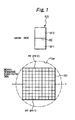
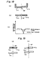
- Figs. 15 and 16 show an example of a conventional exposure apparatus of separate transfer type as mentioned above.
- an electron ray or beam EB emitted from a beam source (not shown) and modified to have square cross-section is deflected to be spaced apart from an optical axis AX of an optical system by a predetermined distance 6 by means of deflectors 1 so that the beam is directed to one of a plurality of small regions or segments 2a formed on a mask 2.
- the small regions 2a include patterns to be transferred to a wafer 5, and the electron beam can pass through each small region.
- the small regions 2a are divided or separated from each other by border zones 2b for shielding or scattering the electron beam.
- the small regions 2a on the mask 2 correspond to the projection or transfer areas 5b on the wafer 5 at a ratio of 1:1.
- the small regions 2a on the mask 2 correspond to the projection or transfer areas 5b on the wafer 5 at a ratio of 1:1.
- the area 5a for one die on the wafer 5 is divided into one hundred transfer areas 5b, one hundred small areas 2a the number of which is equal to that of the areas 5b are formed on the mask 2. Since the pattern is transferred from the mask 2 to the wafer 5 with the reduction ratio, each small region 2a is greater than the corresponding transfer area 5b by the factor corresponding to the reciprocal number of the reduction ratio.
- not only the small regions 2a but also the border zones 2b are formed on the mask 2. Accordingly, as shown in Fig.
Landscapes
- Chemical & Material Sciences (AREA)
- Engineering & Computer Science (AREA)
- Nanotechnology (AREA)
- Analytical Chemistry (AREA)
- Physics & Mathematics (AREA)
- Crystallography & Structural Chemistry (AREA)
- Condensed Matter Physics & Semiconductors (AREA)
- General Physics & Mathematics (AREA)
- Manufacturing & Machinery (AREA)
- Mathematical Physics (AREA)
- Theoretical Computer Science (AREA)
- Electron Beam Exposure (AREA)
Claims (5)
- Übertragungsverfahren mit einem geladenen Teilchenstrahl zur Übertragung eines vorbestimmten Musters auf eine vorbestimmte Fläche auf einem Substrat (101), wobei das an die vorbestimmte Fläche auf dem Substrat (101) zu übertragende Muster in eine Vielzahl von kleinen Bereichen (SF1, SF2) unterteilt wird, die auf einer Maske voneinander beabstandet sind, wobei das Verfahren das wiederholte Ausrichten eines geladenen Teilchenstrahls an die kleinen Bereiche (SF1, SF2) auf der Maske aufweist, und jeder kleine Bereich als eine Einheit der Projektion mit dem Strahl behandelt wird, und die Musterübertragungspositionen dergestalt eingestellt werden, dass die den kleinen Bereichen (SF1, SF2) entsprechenden Übertragungsflächen auf dem Substrat miteinander in Kontakt stehen,
dadurch gekennzeichnet, dass, wenn das an die vorbestimmte Fläche auf dem Substrat zu übertragende Muster in einer Vielzahl von kleinen Bereichen (PF1, PF2) unterteilt wird, die kleinen Bereiche (PF1, PF2) mit dem selben Musterabschnitt nach der Unterteilung durch einen gemeinsamen kleinen Bereich (SF1, SF2) dargestellt werden, und nach der Übertragung das Muster des gemeinsamen kleinen Bereiches (SF1, SF2) auf eine Vielzahl von Positionen auf dem Substrat übertragen wird. - Übertragungsverfahren nach Anspruch 1, bei dem ein maskenseitiges optisches Feld eines in der Übertragung verwendeten optischen Systems kleiner als das maskenseitige optische Feld eingestellt wird, welches benötigt werden würde, wenn der gemeinsame kleine Bereich (SF1, SF2) nicht verwendet wird.
- Übertragungsverfahren nach Anspruch 1, bei dem die vorbestimmte Fläche (111) auf dem Substrat größer als ein substratseitiges optisches Feld (FSw) einer Übertragungsvorrichtung vom geladenen Teilchenstrahltyp in einer Richtung des Substrates eingestellt wird, und nach der Übertragung die kleinen Bereiche (SF1, SF2) auf der Maske auf die vorbestimmte Fläche (111) auf dem Substrat durch Verschieben des Substrates in der einen Richtung übertragen werden.
- Übertragungsverfahren nach Anspruch 1, bei dem die vorbestimmte Fläche (121) auf dem Substrat innerhalb eines substratseitigen optisches Feldes (FSw) einer Übertragungsvorrichtung vom geladenen Teilchenstrahltyp eingestellt wird, und das auf die vorbestimmte Fläche (121) zu übertragende Muster in kleine Bereiche (SF) unterteilt wird, die in einem Bereich (120) liegen, der größer ist als ein maskenseitiges optisches Feld (FSm) der Übertragungsvorrichtung vom geladenen Teilchenstrahltyp in einer Richtung der Maske ist, und bei dem nach der Übertragung der Musterabschnitte der kleinen Bereiche (SF) der Maske auf die vorbestimmte Fläche (121) auf dem Substrat durch Verschieben des Substrates in der einen Richtung übertragen werden.
- Übertragungsverfahren nach Anspruch 1, bei dem die vorbestimmte Fläche (131) auf dem Substrat größer als ein substratseitiges optisches Feld (FSw) einer Übertragungsvorrichtung vom geladenen Teilchenstrahltyp in einer Richtung des Substrates eingestellt wird, und das auf die vorbestimmte Fläche (131) zu übertragende Muster in kleine Bereiche (SF) unterteilt wird, die in einem Bereich (130) liegen, der größer ist als ein maskenseitiges optisches Feld (FSm) der Übertragungsvorrichtung vom geladenen Teilchenstrahltyp in einer Richtung der Maske ist, und bei dem nach der Übertragung der Musterabschnitte der kleinen Bereiche (SF) der Maske auf die vorbestimmte Fläche (131) auf dem Substrat durch Verschieben der Maske in der einen Richtung der Maske und durch Verschieben des Substrates in der einen Richtung übertragen werden.
Priority Applications (2)
| Application Number | Priority Date | Filing Date | Title |
|---|---|---|---|
| EP99109300A EP0949654A3 (de) | 1994-06-16 | 1995-06-16 | Musterübertragungsverfahren mittels Ladungsträgerstrahls |
| EP99109301A EP0949655A3 (de) | 1994-06-16 | 1995-06-16 | Musterübertragungsverfahren mittels Ladungsträgerstrahls |
Applications Claiming Priority (6)
| Application Number | Priority Date | Filing Date | Title |
|---|---|---|---|
| JP13412294 | 1994-06-16 | ||
| JP134122/94 | 1994-06-16 | ||
| JP13412294 | 1994-06-16 | ||
| JP143246/94 | 1994-06-24 | ||
| JP14324694 | 1994-06-24 | ||
| JP14324694 | 1994-06-24 |
Related Child Applications (2)
| Application Number | Title | Priority Date | Filing Date |
|---|---|---|---|
| EP99109300A Division EP0949654A3 (de) | 1994-06-16 | 1995-06-16 | Musterübertragungsverfahren mittels Ladungsträgerstrahls |
| EP99109301A Division EP0949655A3 (de) | 1994-06-16 | 1995-06-16 | Musterübertragungsverfahren mittels Ladungsträgerstrahls |
Publications (3)
| Publication Number | Publication Date |
|---|---|
| EP0688036A2 EP0688036A2 (de) | 1995-12-20 |
| EP0688036A3 EP0688036A3 (de) | 1997-11-26 |
| EP0688036B1 true EP0688036B1 (de) | 2004-05-12 |
Family
ID=26468310
Family Applications (3)
| Application Number | Title | Priority Date | Filing Date |
|---|---|---|---|
| EP99109300A Pending EP0949654A3 (de) | 1994-06-16 | 1995-06-16 | Musterübertragungsverfahren mittels Ladungsträgerstrahls |
| EP95304194A Expired - Lifetime EP0688036B1 (de) | 1994-06-16 | 1995-06-16 | Muster-Übertragungsverfahren mittels eines Ladungsträgerstrahls |
| EP99109301A Pending EP0949655A3 (de) | 1994-06-16 | 1995-06-16 | Musterübertragungsverfahren mittels Ladungsträgerstrahls |
Family Applications Before (1)
| Application Number | Title | Priority Date | Filing Date |
|---|---|---|---|
| EP99109300A Pending EP0949654A3 (de) | 1994-06-16 | 1995-06-16 | Musterübertragungsverfahren mittels Ladungsträgerstrahls |
Family Applications After (1)
| Application Number | Title | Priority Date | Filing Date |
|---|---|---|---|
| EP99109301A Pending EP0949655A3 (de) | 1994-06-16 | 1995-06-16 | Musterübertragungsverfahren mittels Ladungsträgerstrahls |
Country Status (3)
| Country | Link |
|---|---|
| US (1) | US5624774A (de) |
| EP (3) | EP0949654A3 (de) |
| DE (1) | DE69533014D1 (de) |
Families Citing this family (10)
| Publication number | Priority date | Publication date | Assignee | Title |
|---|---|---|---|---|
| US5965327A (en) * | 1991-12-03 | 1999-10-12 | Asahi Kogaku Kogyo Kaisha | Method for manufacturing a master die for a diffusion plate and diffusion manufactured by said method |
| JP3940824B2 (ja) * | 1995-08-14 | 2007-07-04 | 株式会社ニコン | 荷電粒子線によるパターン転写方法および転写装置 |
| US5798194A (en) * | 1996-05-22 | 1998-08-25 | Nikon Corporation | Masks for charged-particle beam microlithography |
| JP2785811B2 (ja) * | 1996-06-27 | 1998-08-13 | 日本電気株式会社 | 電子線露光装置用露光マスクデータの作成方法および電子線露光装置用マスク |
| US6225637B1 (en) * | 1996-10-25 | 2001-05-01 | Canon Kabushiki Kaisha | Electron beam exposure apparatus |
| JPH1126372A (ja) * | 1997-07-08 | 1999-01-29 | Nikon Corp | 縮小転写方法及び縮小転写用マスク |
| US6222197B1 (en) | 1997-08-21 | 2001-04-24 | Nikon Corporation | Charged-particle-beam pattern-transfer methods and apparatus |
| JP3087843B2 (ja) * | 1997-12-26 | 2000-09-11 | 日本電気株式会社 | 電子線直接描画方法および装置ならびに記録媒体 |
| EP1091383A3 (de) * | 1999-10-07 | 2005-01-19 | Lucent Technologies Inc. | Elektronenstrahl-Abbildungsgerät |
| US6528934B1 (en) | 2000-05-30 | 2003-03-04 | Chunghwa Picture Tubes Ltd. | Beam forming region for electron gun |
Family Cites Families (13)
| Publication number | Priority date | Publication date | Assignee | Title |
|---|---|---|---|---|
| JPS593923A (ja) * | 1982-06-30 | 1984-01-10 | Fujitsu Ltd | 電子ビ−ム露光方法 |
| JP2706099B2 (ja) * | 1988-09-06 | 1998-01-28 | 富士通株式会社 | 半導体装置の製造方法 |
| EP0364929B1 (de) * | 1988-10-20 | 1995-09-06 | Fujitsu Limited | Herstellungsverfahren für Halbleitervorrichtungen und durchsichtige Maske für den geladenen Teilchenstrahl |
| US5079112A (en) * | 1989-08-07 | 1992-01-07 | At&T Bell Laboratories | Device manufacture involving lithographic processing |
| US5258246A (en) * | 1989-08-07 | 1993-11-02 | At&T Bell Laboratories | Device manufacture involving lithographic processing |
| US5130213A (en) * | 1989-08-07 | 1992-07-14 | At&T Bell Laboratories | Device manufacture involving lithographic processing |
| JPH0744145B2 (ja) * | 1989-12-12 | 1995-05-15 | 株式会社東芝 | 電子ビーム露光方法及びその装置 |
| US5227269A (en) * | 1990-06-22 | 1993-07-13 | Texas Instruments Incorporated | Method for fabricating high density DRAM reticles |
| JP3105580B2 (ja) * | 1991-07-29 | 2000-11-06 | 富士通株式会社 | 荷電粒子線描画用マスク作成方法及びマスク |
| US5260151A (en) * | 1991-12-30 | 1993-11-09 | At&T Bell Laboratories | Device manufacture involving step-and-scan delineation |
| JPH05267142A (ja) * | 1992-03-17 | 1993-10-15 | Hitachi Ltd | 電子線描画装置 |
| US5189306A (en) * | 1992-03-24 | 1993-02-23 | International Business Machines Corporation | Grey-splice algorithm for electron beam lithography post-processor |
| US5279925A (en) * | 1992-12-16 | 1994-01-18 | At&T Bell Laboratories | Projection electron lithographic procedure |
-
1995
- 1995-06-15 US US08/490,579 patent/US5624774A/en not_active Expired - Fee Related
- 1995-06-16 DE DE69533014T patent/DE69533014D1/de not_active Expired - Lifetime
- 1995-06-16 EP EP99109300A patent/EP0949654A3/de active Pending
- 1995-06-16 EP EP95304194A patent/EP0688036B1/de not_active Expired - Lifetime
- 1995-06-16 EP EP99109301A patent/EP0949655A3/de active Pending
Also Published As
| Publication number | Publication date |
|---|---|
| EP0688036A2 (de) | 1995-12-20 |
| EP0949654A2 (de) | 1999-10-13 |
| EP0949655A2 (de) | 1999-10-13 |
| US5624774A (en) | 1997-04-29 |
| EP0949655A3 (de) | 2001-04-04 |
| EP0949654A3 (de) | 2001-01-31 |
| EP0688036A3 (de) | 1997-11-26 |
| DE69533014D1 (de) | 2004-06-17 |
Similar Documents
| Publication | Publication Date | Title |
|---|---|---|
| JP3940824B2 (ja) | 荷電粒子線によるパターン転写方法および転写装置 | |
| KR100961019B1 (ko) | 묘화 방법 및 하전 입자 빔 묘화 장치 | |
| US5376802A (en) | Stencil mask and charge particle beam exposure method and apparatus using the stencil mask | |
| JPS63114125A (ja) | 荷電ビ−ム露光装置 | |
| JPH10335215A (ja) | 荷電粒子線描画装置 | |
| USRE44179E1 (en) | Charged particle beam writing method | |
| JP3601630B2 (ja) | 荷電粒子線転写方法 | |
| JPH11204422A (ja) | 荷電粒子線転写方法 | |
| EP0688036B1 (de) | Muster-Übertragungsverfahren mittels eines Ladungsträgerstrahls | |
| JPH0864522A (ja) | 荷電粒子線転写方法 | |
| US20030194652A1 (en) | Charged-particle-beam microlithography apparatus and methods for exposing a segmented reticle | |
| US6087669A (en) | Charged-particle-beam projection-microlithography apparatus and transfer methods | |
| US6764925B2 (en) | Semiconductor device manufacturing system and electron beam exposure apparatus | |
| US5847402A (en) | Charged particle beam pattern transfer apparatus and method | |
| KR100379290B1 (ko) | 전자빔 노광용 마스크와 이를 이용한 반도체 장치 제조 방법 | |
| JP4468752B2 (ja) | 荷電粒子線露光方法、荷電粒子線露光装置及びデバイス製造方法 | |
| JPH08236428A (ja) | 荷電粒子線露光方法及びそれに用いるマスク | |
| US6335127B1 (en) | Charged beam mask having strut wider than charged beam, with shape that matches charged beam | |
| JP3336510B2 (ja) | パターン転写方法およびそれに用いる装置並びにマスク | |
| JP2005302868A (ja) | 電子ビーム描画方法および装置 | |
| US6300023B1 (en) | Microlithographic pattern-transfer methods for large segmented reticles, and device manufacturing methods using same | |
| WO2002103764A1 (en) | Electron beam exposure system | |
| JPH1079346A (ja) | 荷電粒子線転写装置 | |
| JP2898726B2 (ja) | 荷電粒子ビーム露光方法 | |
| KR100453016B1 (ko) | 하전입자선에의한패턴전사및전사장치 |
Legal Events
| Date | Code | Title | Description |
|---|---|---|---|
| PUAI | Public reference made under article 153(3) epc to a published international application that has entered the european phase |
Free format text: ORIGINAL CODE: 0009012 |
|
| AK | Designated contracting states |
Kind code of ref document: A2 Designated state(s): DE FR GB |
|
| PUAL | Search report despatched |
Free format text: ORIGINAL CODE: 0009013 |
|
| AK | Designated contracting states |
Kind code of ref document: A3 Designated state(s): DE FR GB |
|
| 17P | Request for examination filed |
Effective date: 19980515 |
|
| 17Q | First examination report despatched |
Effective date: 19980915 |
|
| GRAP | Despatch of communication of intention to grant a patent |
Free format text: ORIGINAL CODE: EPIDOSNIGR1 |
|
| GRAS | Grant fee paid |
Free format text: ORIGINAL CODE: EPIDOSNIGR3 |
|
| GRAA | (expected) grant |
Free format text: ORIGINAL CODE: 0009210 |
|
| AK | Designated contracting states |
Kind code of ref document: B1 Designated state(s): DE FR GB |
|
| PG25 | Lapsed in a contracting state [announced via postgrant information from national office to epo] |
Ref country code: FR Free format text: LAPSE BECAUSE OF FAILURE TO SUBMIT A TRANSLATION OF THE DESCRIPTION OR TO PAY THE FEE WITHIN THE PRESCRIBED TIME-LIMIT Effective date: 20040512 |
|
| REG | Reference to a national code |
Ref country code: GB Ref legal event code: FG4D |
|
| REF | Corresponds to: |
Ref document number: 69533014 Country of ref document: DE Date of ref document: 20040617 Kind code of ref document: P |
|
| PGFP | Annual fee paid to national office [announced via postgrant information from national office to epo] |
Ref country code: DE Payment date: 20040624 Year of fee payment: 10 |
|
| PG25 | Lapsed in a contracting state [announced via postgrant information from national office to epo] |
Ref country code: DE Free format text: LAPSE BECAUSE OF FAILURE TO SUBMIT A TRANSLATION OF THE DESCRIPTION OR TO PAY THE FEE WITHIN THE PRESCRIBED TIME-LIMIT Effective date: 20040813 |
|
| PLBE | No opposition filed within time limit |
Free format text: ORIGINAL CODE: 0009261 |
|
| STAA | Information on the status of an ep patent application or granted ep patent |
Free format text: STATUS: NO OPPOSITION FILED WITHIN TIME LIMIT |
|
| 26N | No opposition filed |
Effective date: 20050215 |
|
| EN | Fr: translation not filed | ||
| PGFP | Annual fee paid to national office [announced via postgrant information from national office to epo] |
Ref country code: GB Payment date: 20050615 Year of fee payment: 11 |
|
| RIN2 | Information on inventor provided after grant (corrected) |
Inventor name: OKINO, TERUAKI |
|
| PG25 | Lapsed in a contracting state [announced via postgrant information from national office to epo] |
Ref country code: GB Free format text: LAPSE BECAUSE OF NON-PAYMENT OF DUE FEES Effective date: 20060616 |
|
| GBPC | Gb: european patent ceased through non-payment of renewal fee |
Effective date: 20060616 |